1. Introduction
Exoplanetary searches have increased in importance in recent years, due to advancements in the interferometric detection techniques outside of the Earth’s atmosphere [
1,
2,
3]. However, these techniques require a high angular resolution and a high sensitivity towards signals buried in noise, as well as a well-defined spectral bandwidth and resolution [
4]. Micro-lens arrays can improve some parameters of IR detectors for the IR interferometry, and reduce problems originating inside the optical system, such as wavefront correction and issues with the field of view (FOV), to name a few [
5,
6,
7].
Micro-lens arrays are arrangements of small-size lenses, called lenslets, distributed side by side to cover the surface of a CCD sensor, where portability is mandatory. A lenslet generally has a circular aperture, due to its easy construction. However, this circular aperture includes a non-active area in the array, due to the distance between two lenslets, that results in an efficiency deterioration. Furthermore, part of the radiation is incident out-of-focus on another pixel, producing crosstalk. Some of the design parameters, such as the radius of curvature, the geometry of the aperture, and the lens material, may be analyzed using a finite element method (FEM). This procedure was employed recently to evaluate the aberrations and the spot in the focal plane.
In this paper, we present a numerical analysis, based on FEM, for a micro-lens array with two different apertures—circular and square—and two radii of curvature. The analysis was performed on an MIR wavelength, used in exoplanetary detection,
λi = 9.492 μm [
8].
2. Materials and Methods
Each lenslet was a convexo-planar lens, due to their easy fabrication. We performed two numerical studies for two different types of lenslet apertures (circular and square) and two frontal radii of curvature.
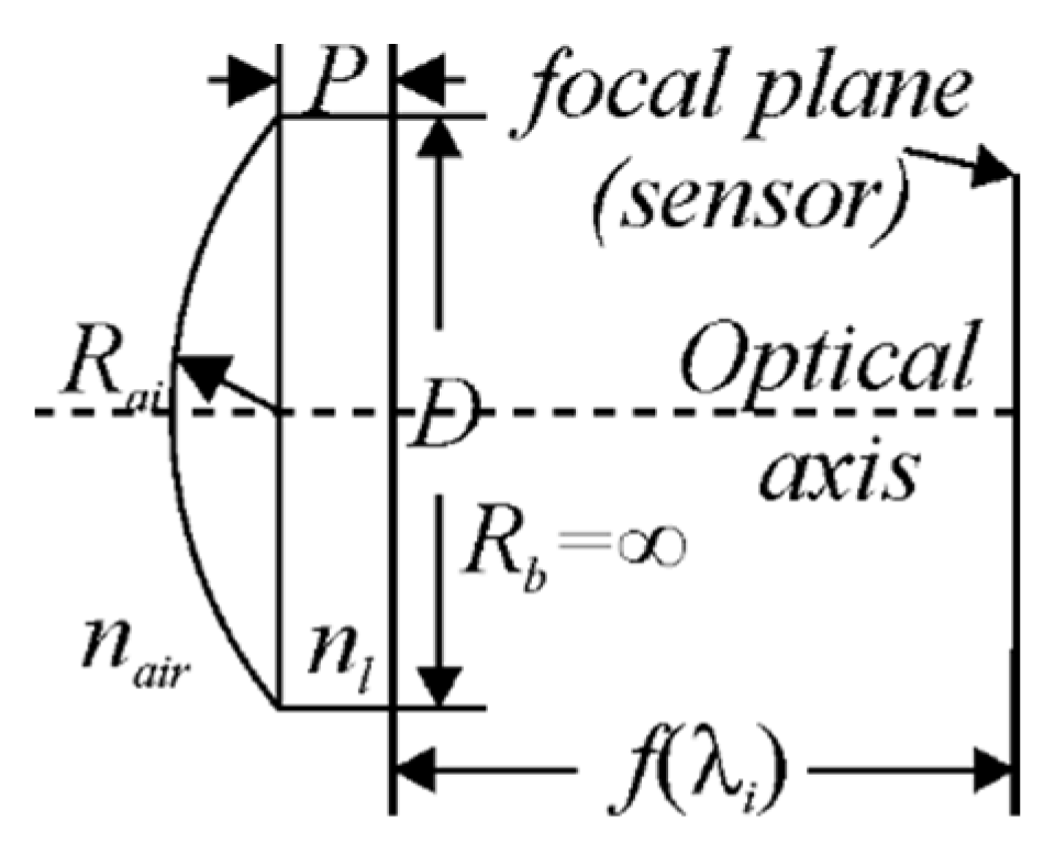
Figure 1 shows a single lenslet of the array. The focal plane located at the focal distance for the test wavelength
f(
λi) represents the sensor surface. The lens maker’s formula indicates the focal length as a function of the radii of curvature,
Rai and
Rb, the refractive index for lens material and surrounding medium,
n(
λi), and
n(
λs), respectively, and the micro-lens thickness,
P. Here, β = n(λi) − n(λs). Equation (1) is valid for any wavelength, refractive indices, and radii of curvature of the lens. In our case, the source wavelength was λi = 9.492 μm, corresponding to the mean wavelength for exoplanetary exploration. The surrounding material was vacuum (n(λs) = 1), and the lens material was Ge (n(λi) = 4.0044). Rai was the radius of curvature for the front surface, with values of Ra1 = 3.7 μm for study one, and Ra2 = 7.4 μm for study two. The radius of the curvature for the back surface was Rb = ∞ for both studies, considering that this surface was flat. The lenslet thickness was P = 3.7 μm, which corresponded to the minimum commercial size. The aperture D = 2Ra1 had a circular shape for study one, and a square shape with sides equal to Ra2 for study two.
Figure 2 shows the micro-lens arrangements for the two cases of studies. The total size of the array corresponded to one-tenth of the commercial dimensions of the CCD sensor, with 160 × 120 pixels. Each pixel had dimensions 7.4 × 7.4 µm, or 118.4 × 88.8 µm for 16 × 12 pixels. We planned for 10 × 10 sub-arrays of micro-lenses, joined side by side, to complete the minimum size for the sensor surface. The aperture for study one was circular, as shown in
Figure 2a. The lenslet in study two was square in form, as shown in
Figure 2b. The geometric aperture changes between the studies had the purpose of decreasing the non-active area between the micro-lenses where the light was incident, but was not imaged on the sensor surface.
The FEM model used in this investigation is described in [
9]. The Zernike polynomials in their polar form with
σ as the radial distance, are shown in [
10]. The non-polarized light source modeled had
λi = 9.492 μm, placed at 15 μm from the lenslet surface, a spot radius of about 44.4 μm, an intensity of 3.18 [mW/cm
2], and an hexapolar normal distribution.
3. Results
A finite element simulation was performed for each case study, employing the same wavelength, initial, and boundary conditions. In study one, the lenses had a circular aperture and a curvature radius of 3.7 μm. In study two, the lenses had a square aperture to avoid non-active areas, and a curvature radius of 7.4 μm.
3.1. RMS Spot Size
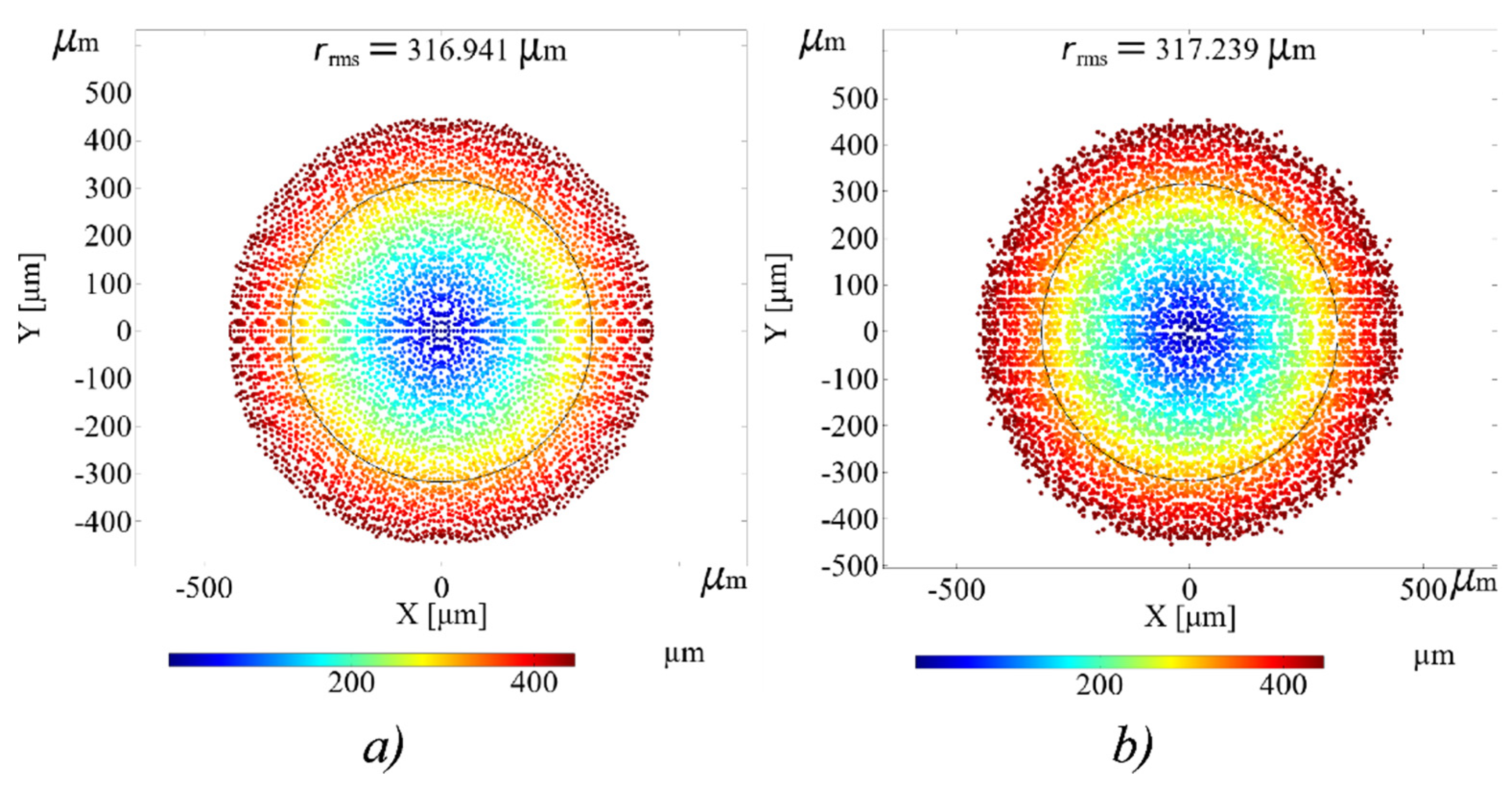
Figure 3 shows the spots at the focal plane for case studies one and two. A black circle indicates the root mean square value of the radius of the spot. The colors represent the ray as a function of the traveled distance from the source. This representation implies the energy distribution, and which rays contributed to the wavefront and crosstalk error. The RMS spot radius for case one (the square aperture) was only 298 nm larger than for case two (circular aperture). This difference indicated that there was no apparent change in the image on the sensor surface using a square aperture. However, when using the square aperture, more energy was concentrated on the sensor surface by filling in the non-active regions, improving the image quality. Moreover, the light focusing efficiency was almost the same for studies one and two, with values of 33.44% and 33.41%, respectively.
3.2. Optical Aberrations
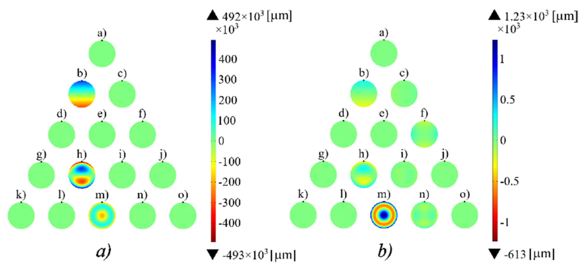
Figure 4 shows the aberrations for case studies one and two. The piston and defocus aberrations have been eliminated because their contribution may have been eliminated during alignment. The values shown in the legend are the wavefront error in μm. As expected, the wavefront errors for study two were smaller than for study one; 400 times lower for the maximum error (dark blue) and 804 times smaller for the minimum error (dark red).
The vertical aberration tilt, vertical coma, and spherical aberration were the most significant in comparison to the other aberrations in both studies. However, the vertical tilt aberration can be corrected by alignment, and does not affect the image quality. The vertical coma aberration indicated a difference in the radii of curvature between the periphery and the central zones. As expected, the vertical coma was not significant in case two. Finally, the spherical aberration indicated the difference between the focal lengths for the periphery and the center. As shown in
Figure 4a, the error was concentrated at the center and the border. Nevertheless, as shown in
Figure 4b, the relative error was distributed over the entire micro-lens array. However, these were smaller in magnitude for the second case than for the first case in study one.
4. Conclusions
The FEM analysis applied for the determination of the aberration and the focal image at the sensor surface produced by a micro-lens array is a valuable tool in lenslet design. The micro-lens array with the square lenslet aperture reduced the crosstalk and results in a decreasing wavefront error, by eliminating the non-active surface areas between lenslets. FEM analysis allows for the optimization of optical design to improve IR detection in interferometric systems.
Author Contributions
Conceptualization, R.G.-R., and G.G.-T.; methodology, R.G.-R.; validation, M.S., G.G.-T.; formal analysis, R.G.-R., and M.S.; investigation, R.G.-R., and G.G.-T.; writing—original draft preparation, R.G.-R., G.G.-T., and M.S.; writing—review and editing, R.G.-R., G.G.-T., and M.S. All authors have read and agreed to the published version of the manuscript.
Funding
This research was funded by Air Force Office of Scientific Research, grant number FA9550-18-1-0454.
Data Availability Statement
The data presented in this study are available upon request from the corresponding author.
Acknowledgments
The author Gonzalez-Romero acknowledges the scholarship of the Consejo Nacional de Ciencia y Tecnología (CONACYT), as well as the Universidad de Guadalajara, for the support to accomplish this research. Special thanks to Adriana Carrillo for their guidance.
Conflicts of Interest
The authors declare no conflict of interest.
References
- Gonzalez-Romero, R.; Strojnik, M.; Garcia-Torales, G.; Gomez-Rosas, G. Frequency Dependence of a Piezo-Resistive Method for Pressure Measurements of Laser-Induced Shock Waves in Solids. Photonics 2021, 8, 120. [Google Scholar] [CrossRef]
- Galan, M.; Strojnik, M.; Garcia-Torales, G.; Kirk, M.S. Telescope Array for Extrasolar Planet Detection from the Far Side of the Moon. Appl. Opt. 2016, 55, D173–D180. [Google Scholar] [CrossRef] [PubMed]
- Strojnik, M.; Scholl, M.K. Extrasolar Planet Observatory on the Far Side of the Moon. J. Appl. Remote Sens. 2014, 8, 1–9. [Google Scholar] [CrossRef]
- Montes-Flores, M.; Garcia-Torales, G.; Strojnik, M. A Lab Proof-of-Concept of an Extrasolar Planet Detection Using a Rotationally Shearing Interferometer. Proc. SPIE 2021, 11830, 118300O. [Google Scholar]
- Leger, J.R.; Scott, M.L.; Bundman, P.; Griswold, M.P. Astigmatic Wavefront Correction of a Gain-Guided Laser Diode Array Using Anamorphic Diffractive Microlenses. In Computer-Generated Holography II; Lee, S.H., Ed.; SPIE: Los Angeles, CA, USA, 1988; Volume 0884, pp. 82–89. [Google Scholar]
- Ratcliff, J.; Supikov, A.; Alfaro, S.; Azuma, R. ThinVR: Heterogeneous Microlens Arrays for Compact, 180 Degree FOV VR near-Eye Displays. IEEE Trans. Vis. Comput. Graph. 2020, 26, 1981–1990. [Google Scholar] [CrossRef] [PubMed]
- Scholl, M.S. Optical Analysis of Segmented Aperture Averager; SPIE: Los Alamos, CA, USA, 1981; Volume 0288. [Google Scholar]
- Strojnik, M. Optimal Wavelength Interval for Extra-Solar Planet Detection; SPIE: San Diego, CA, USA, 2021; Volume 11830. [Google Scholar]
- Gonzalez-Romero, R.; García-Torales, G.; Strojnik, M. Spatial Distribution Analysis of Two-Dimensional Microlens Arrays by Finite Element Method; SPIE: San Diego, CA, USA, 2021; Volume 11830. [Google Scholar]
- Lakshminarayanan, V.; Fleck, A. Zernike Polynomials: A Guide. J. Mod. Opt. 2011, 58, 545–561. [Google Scholar] [CrossRef]
| Publisher’s Note: MDPI stays neutral with regard to jurisdictional claims in published maps and institutional affiliations. |
© 2021 by the authors. Licensee MDPI, Basel, Switzerland. This article is an open access article distributed under the terms and conditions of the Creative Commons Attribution (CC BY) license (https://creativecommons.org/licenses/by/4.0/).


