Abstract
This research aims to determine an optimized set of parameters for Altium Designer’s built-in autorouting function when applied on two- or more-layer printed circuit board (PCB) designs. An experimental approach is employed, creating a specific PCB layout with pre-placed components. The autorouting function is utilized to generate trace connections between components, with different parameter settings being tested to assess their impact on routing quality, efficiency, and speed. Routing time will be a key metric measured during this evaluation. The resulting autorouted designs will then be compared to a manually routed PCB designed by an engineer, considering factors such as routing neatness and adherence to design rules. This research aims to determine the effectiveness of the autorouting tool in PCB designs while potentially reducing design time.
1. Introduction
The design of printed circuit boards (PCBs) has been a time-consuming and precision-demanding engineering task since its inception. This is due to the unique nature of electronic rules and design patterns for each panel and target hardware. With the advent of PCB manufacturing and the electronics revolution in the 1960s, automation efforts began to emerge hand in hand, with one of the key goals being to replace time-consuming workflows, such as routing. The earliest algorithms and software implementations employed the Lee algorithm, followed by the development of numerous partial or complete solutions to address routing challenges. Even before the 2000s, it became evident that autorouting was not a universal solution for all PCB design tasks [1,2,3,4].
The primary objective of this research is to demonstrate, in multiple steps, the point at which the size of the panel, the number of components, or the complexity of the logical network exceed a certain threshold, rendering the automated routing result significantly less efficient than manual routing in terms of engineering time savings. Additionally, the research aims to identify a set of parameters that can yield satisfactory results for panels of a given size, requiring minimal post-processing by the engineer.
2. Materials and Methods
Recent research has explored the development of novel algorithms that employ various mathematical models to address the challenge of connecting electronic components, such as those arranged in a triangular grid [5]. Another study successfully implemented an algorithm based on dilation and erosion morphological operations to perform component routing [6].
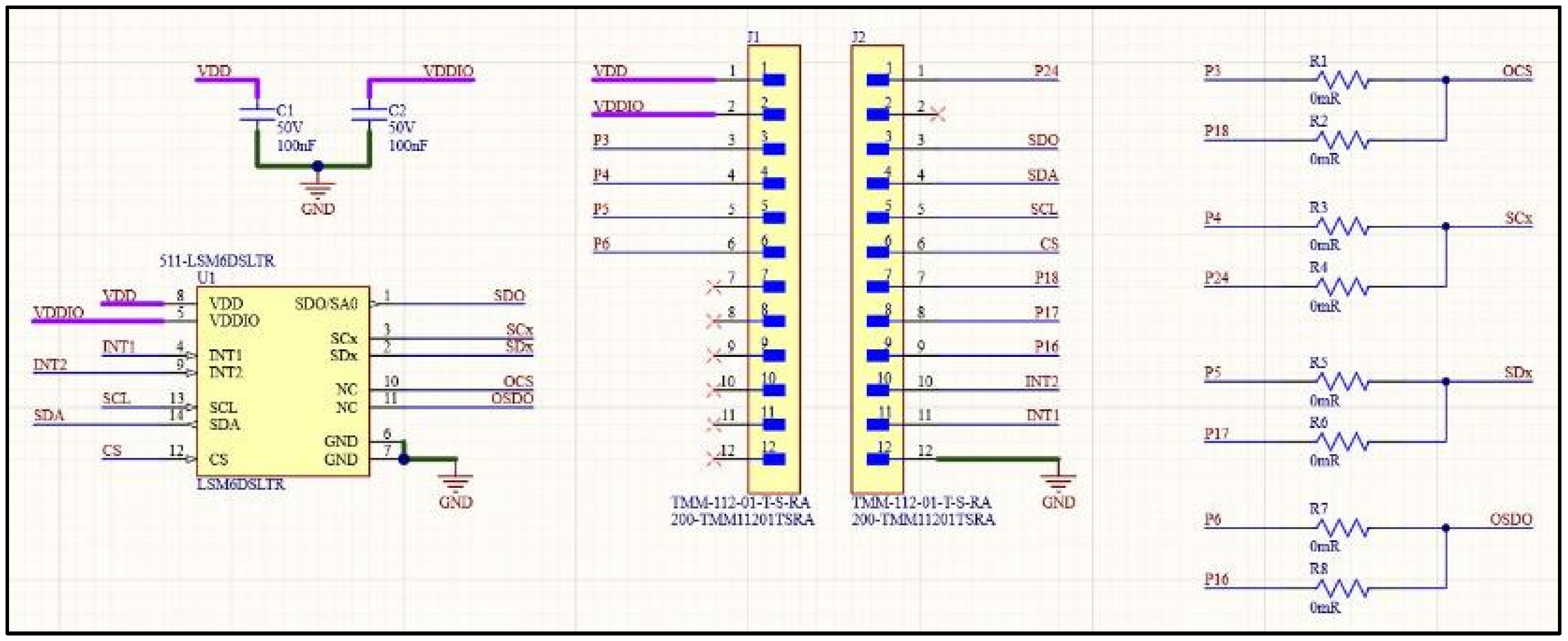
Furthermore, another research has investigated not only routing optimization but also component placement and panel size optimization, employing a genetic algorithm to determine the ideal placement of components and then route between their logical connections [7,8]. Self-organizing genetic algorithm [4] and the proposed algorithm of Zinnatova and Suzdalcev [9] consider heat transfer and dissipation as a main optimization objective. While the above-mentioned algorithms can effectively optimize the design space and ensure uniform heat distribution, the resulting solutions often entail significant compromises in terms of functionality compared to experienced engineering designs, which consider numerous additional factors, such as reliability, manufacturability, and even EMC guidelines. In contrast to examining individual components or proper heat transfer as an optimization target, my research entails evaluating algorithms and their settings by implementing them on an entire PCB project and comparing the outcomes. The circuit schematic (Figure A1) comprised 13 components and 21 network elements. Based on a STMicroelectronics evaluation board as a reference, I assigned the board dimensions to be 25 mm × 25 mm. The components included 2 through-hole connectors and 11 surface-mount components, consisting of 1 integrated circuit and 10 passive components. Manual placement is key for the perfect functionality, so I placed the components and the keep-out layer primitives on my experimental board, which defined the boundary conditions for the automated routing algorithms in Altium Designer. Designing the component placement and board settings for single-sided assembly took 10 min.
The experimental setup included both two-layer and four-layer configurations with different algorithm options and settings, where the predefined result parameters would be:
- Running time;
- Number of Design Rule Check (DRC) violations evaluated with the sophisticated built-in function of Altium Designer;
- Number of Track and Pad corner connections;
- 90° track corners;
- Number of Vias.
3. Results
3.1. Default and Orthogonal Two-Layer Autorouting Results Regarding Clearance
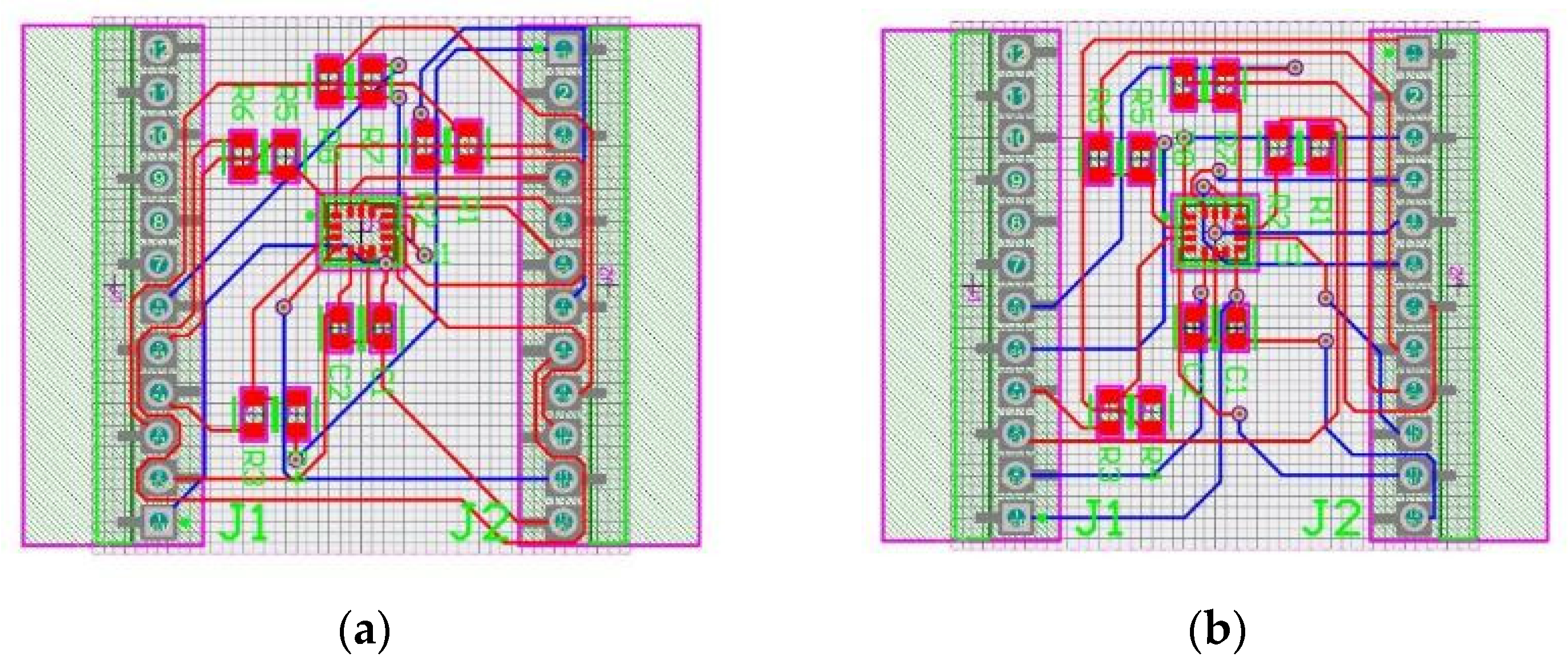
I have created a two-layer PCB design layout, where the same default algorithm has been running; the only difference is that (Figure 1) the clearance of the components, traces, and vias have been increased in the rules. That change modified a lot in the autoroute and increased the number of used vias from 8 to 10.
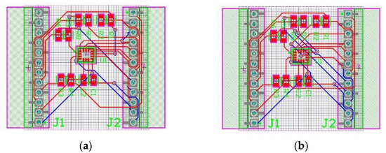
Figure 1.
(a) Default two-layer autorouting result with 0.15 mm clearance; (b) default two-layer autorouting result with 0.2 mm clearance.
During the orthogonal design phase, the above adjustments implemented did not significantly alter the routing. However, the initial number of vias decreased from 13 to 11 upon increasing the clearance between the elements.
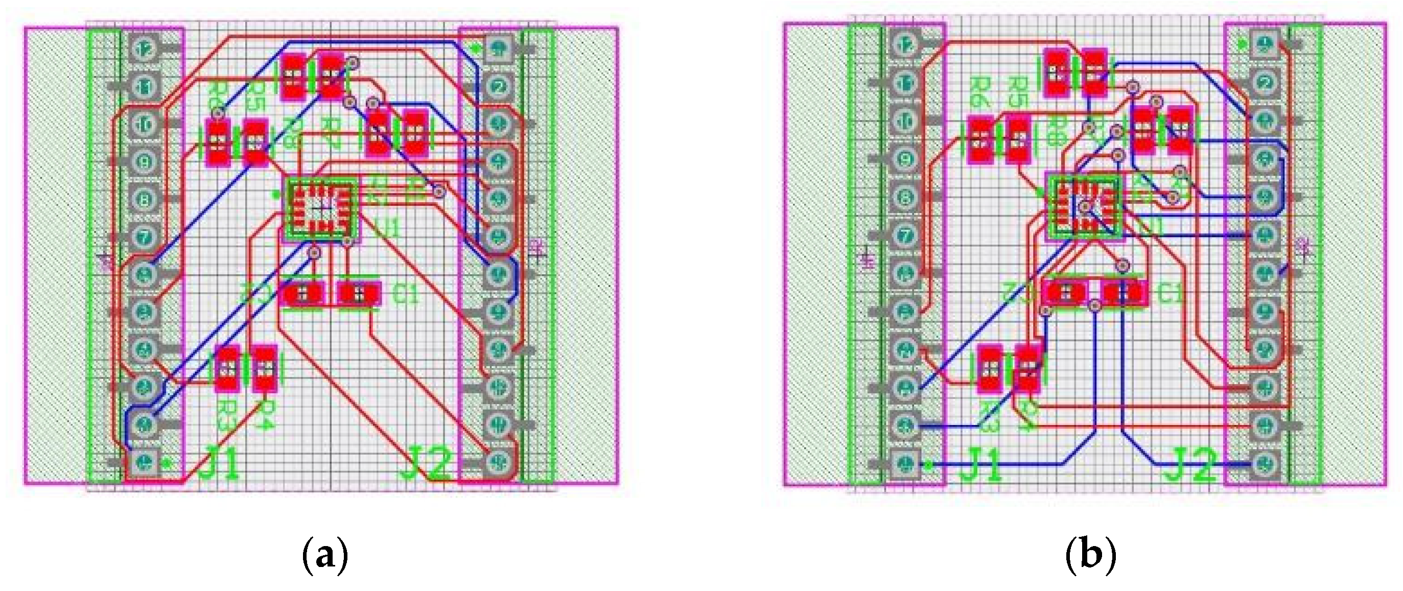
3.2. Orthogonal and Default Strategy Comparison in Layout 2
Orthogonal routing strategy shows a lot of differences which could be explained with the main differences of the algorithms in the background. While the default strategy is working in a continuous space, the orthogonal routing algorithm operates in a discrete grid. Distance metric is also a key difference between the two algorithms, as the orthogonal router uses Manhattan distance formula:
While default routing uses Euclidean distance calculations [10].
While the orthogonal layout (Figure 2) provides a more aesthetically pleasing appearance, it necessitates a higher number of vias and longer traces. However, this factor does not significantly impact the results of this study, as the panel size and functionality are predetermined, and there is no requirement for high-speed signal transmission.
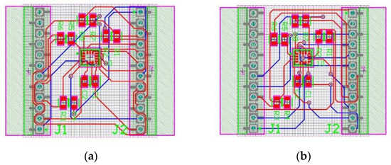
Figure 2.
(a) Default two-layer autorouting result with 0.2mm clearance; (b) orthogonal autorouting result with 0.2 mm clearance.
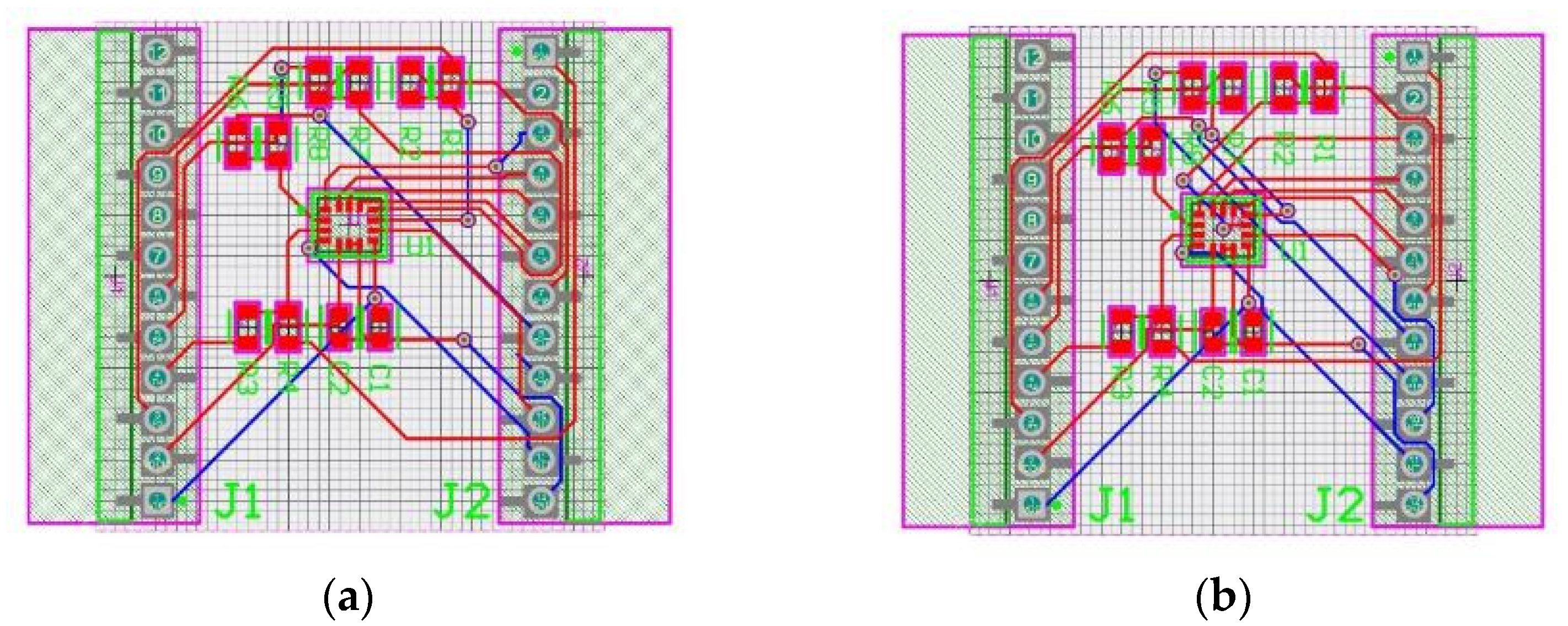
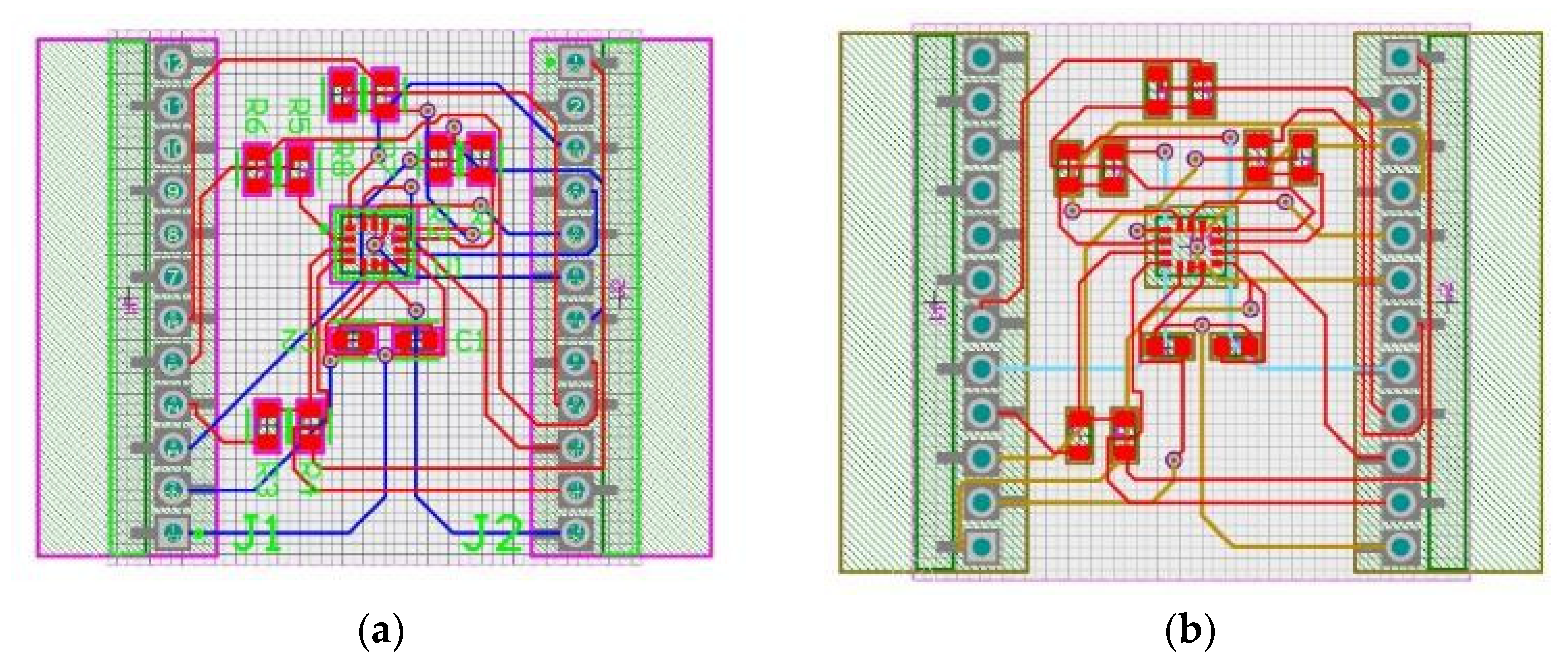
3.3. Default and Orthogonal Strategy Comparison in Layout Three
To assess the impact of component placement on routing complexity, I modified the layout by rotating capacitors C1 and C2. This modification can also be beneficial for manual placement. The default router successfully routed the layout with seven vias, while orthogonal routing required 11 vias. Overall, component rotation did not significantly affect the routing design (Figure 3).
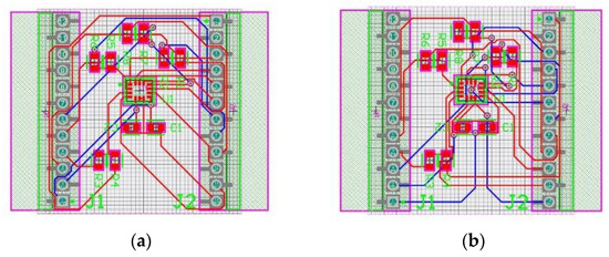
Figure 3.
(a) Default autorouting result in layout three with 0.2 mm clearance; (b) orthogonal autorouting result in layout three with 0.2 mm clearance.
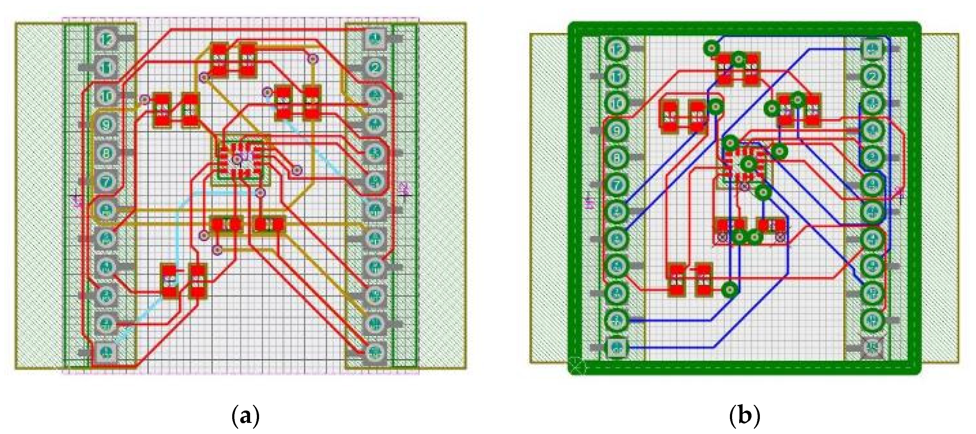
3.4. Two- and Four-Layer Autorouting Result Comparison
To align with industry standards, I experimented with a four-layer PCB stack, even though the component count did not necessitate it. Routing algorithms typically consider trace collisions, so additional layers can facilitate a more organized board layout in constrained spaces. Figure 4 compares two- and four-layer routing without any specific plane settings. With the option of multiple layers, the algorithm utilized three layers, resulting in a reduction of one via.
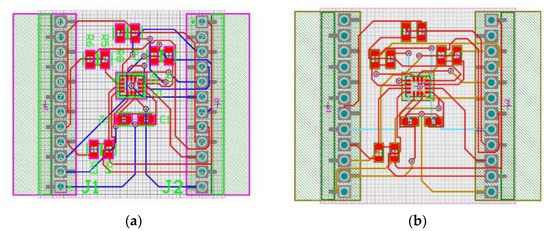
Figure 4.
(a) Two-layer design result of the orthogonal autorouting; (b) four-layer routing result with multilayer routing algorithm.
3.5. Multi-Layer Autorouting Comparison Regarding Inner Plane Presence
There is a specific PCB stack setting which has a huge impact on the design regardless of the algorithm and the operator. If the PCB stack allows for signaling in the inner layers, then routing algorithms could use that to create traces and connect any points within the design. If the inner layers are considered as planes, then only one specific net could use that. In that case, all the algorithms and a manual router must solve another problem. In my case, I defined the inner planes as GND. The following result (Figure 5) shows that the number of vias increased by 66% if GND planes were included in the design.
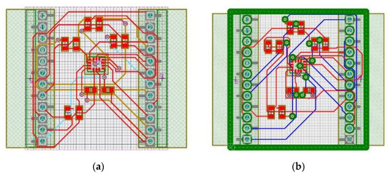
Figure 5.
(a) Multilayer autorouting solution without GND planes; (b) multilayer autorouting solution with specified GND planes.
The following table (Table 1) presents all the statistical data collected during this experimental research.

Table 1.
Comparison table for autorouting strategies and evaluation metrics.
4. Conclusions
The research demonstrated the feasibility of automated routing for PCB projects with a small number of logical connections, significantly reducing engineering hours. Even considering the time required for manual preparation, a 16-min manual task was completed in under four seconds in the worst-case scenario. Accounting for potential error correction, a 16 min task could still be completed in under 8 min, potentially achieving a 50% time saving. The research results indicate that the introduction of inner layers leads to an increase in the number of vias. During the initial stages of the research, it became apparent that the algorithms required spacings exceeding the manufacturing tolerances (minimum 0.2 mm) to prevent DRC errors. This practical insight can be valuable for optimizing the design process.
The advanced routing algorithm used in this research for multi-layer PCBs employs a seven-step process with seven additional customization options. While the built-in orthogonal algorithm may encounter DRC errors, it demonstrated superior performance in two instances, producing DRC-free results. This suggests its potential as a reference for future research and parameter optimization. Further investigation is needed to compare the applied algorithms and a new customized algorithm.
To further advance this research, I propose three key initiatives: investigate at least two additional test panels with a larger component count, involve additional researchers to evaluate manual routing time, and develop a customized algorithm to enhance automated routing results.
Funding
Project no. TKP2021-NVA-23 has been implemented with the support provided by the Ministry of Technology and Industry of Hungary from the National Research, Development and Innovation Fund, financed under the TKP2021-NVA funding scheme.
Institutional Review Board Statement
Not applicable.
Informed Consent Statement
Not applicable.
Data Availability Statement
The raw data supporting the conclusions of this article will be made available by the authors on request.
Conflicts of Interest
The author declares no conflict of interest.
Appendix A
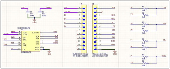
Figure A1.
Schematic diagram of the test panel.
Figure A1.
Schematic diagram of the test panel.
References
- Hu, J.; Sapatnekar, S.S. A survey on multi-net global routing for integrated circuits. Integration 2001, 31, 1–49. [Google Scholar] [CrossRef]
- Kong, H.; Yan, T.; Wong, M.D.F. Automatic bus planner for dense PCBs. In Proceedings of the 46th Annual Design Automation Conference (DAC ‘09), San Francisco, CA, USA, 26–31 July 2009; pp. 326–331. [Google Scholar] [CrossRef]
- Wu, P.-C.; Ma, Q.; Wong, M.D.F. An ILP-based automatic bus planner for dense PCBs. In Proceedings of the 2013 18th Asia and South Pacific Design Automation Conference (ASP-DAC), Yokohama, Japan, 22–25 January 2013; pp. 181–186. [Google Scholar] [CrossRef]
- Ozdal, M.M.; Wong, M.D.F. A Length-Matching Routing Algorithm for High-Performance Printed Circuit Boards. IEEE Trans. Comput.-Aided Des. Integr. Circuits Syst. 2006, 25, 2784–2794. [Google Scholar] [CrossRef]
- Chen, J.; Zhou, Y.; Liu, Q.; Zhang, X. A Novel Global Routing Algorithm for Printed Circuit Boards Based on Triangular Grid. Electronics 2023, 12, 4942. [Google Scholar] [CrossRef]
- Álvarez Mata, L.C.; Rojas Fernández, J.C. PCB Auto Routing Algorithm Based on Morphological Operations. In Proceedings of the 2023 IEEE MTT-S Latin America Microwave Conference (LAMC), San José, Costa Rica, 6–8 December 2023; pp. 113–116. [Google Scholar] [CrossRef]
- Badriyah, T.; Setyorini, F.; Yuliawan, N. The implementation of Genetic Algorithm and Routing Lee for PCB design optimization. In Proceedings of the International Conference on Informatics and Computing (ICIC), Mataram, Indonesia, 28–29 October 2016; pp. 148–153. [Google Scholar] [CrossRef]
- Lin, S.-T.; Wang, H.-H.; Kuo, C.-Y.; Chen, Y.; Li, Y.-L. A Complete PCB Routing Methodology with Concurrent Hierarchical Routing. In Proceedings of the 2021 58th ACM/IEEE Design Automation Conference (DAC), San Francisco, CA, USA, 5–9 December 2021; pp. 1141–1146. [Google Scholar] [CrossRef]
- Zinnatova, L.I.; Suzdalcev, I.V. Optimization of Electronics Component Placement Design on PCB Using Genetic Algorithm. In Proceedings of the SYRCoSE Software Engineering Colloquium, Kazan, Russia, 30–31 May 2013. [Google Scholar] [CrossRef]
- Singh, A.; Yadav, A.; Rana, A. K-means with Three different Distance Metrics. Int. J. Comput. Appl. 2013, 67, 13–17. [Google Scholar] [CrossRef]
Disclaimer/Publisher’s Note: The statements, opinions and data contained in all publications are solely those of the individual author(s) and contributor(s) and not of MDPI and/or the editor(s). MDPI and/or the editor(s) disclaim responsibility for any injury to people or property resulting from any ideas, methods, instructions or products referred to in the content. |
© 2024 by the author. Licensee MDPI, Basel, Switzerland. This article is an open access article distributed under the terms and conditions of the Creative Commons Attribution (CC BY) license (https://creativecommons.org/licenses/by/4.0/).