Abstract
The existing instruments for aerodynamic pressure measurements are usually built around an array of discrete pressure sensors, placed in the same housing together with a few discrete temperature sensors. However, this approach is limiting, especially regarding miniaturization, sensor matching, and thermal coupling. In this work, we intend to overcome these limitations by proposing a novel MEMS multisensor chip, which has a monolithically integrated matrix of four piezoresistive MEMS pressure-sensing elements and two resistive temperature-sensing elements. After finishing the preliminary chip design, we performed computer simulations in order to assess its mechanical behavior when measured pressure is applied. Subsequently, the final chip design was completed, and the first batch was fabricated. The used technological processes included photolithography, thermal oxidation, diffusion, sputtering, micromachining (wet chemical etching), anodic bonding, and wafer dicing.
1. Introduction
Sensors that belong to micro-electromechanical systems (MEMS) constitute one of the most popular and promising classes of sensors. MEMS sensors are miniature sensing devices fabricated using microelectronic and micromachining technologies. First appearing shortly after the development of monolithic integrated circuits in the 1960s, they have been adopted for a wide range of applications during the decades since. Today, they are indispensable in vehicles, medical devices, mobile phones, and many other modern industrial and commercial applications. Piezoresistive MEMS pressure sensors constitute a large portion of the MEMS sensor market today, with the demand for them still growing. They have significant advantages over other types of pressure sensors, including miniature dimensions, good measurement performance, high reliability, and low cost due to efficient mass production. Although piezoresistive MEMS pressure sensors may nowadays be considered a mature technology, new applications continue to arise, and there are new scientific and technological challenges to be addressed [1,2].
The aerodynamic testing of various objects is often performed by measuring pressure at a multitude of points on aerodynamic surfaces or structural elements. Typically, the air pressure from the measurement points is transferred via flexible tubing to multichannel pressure-sensing instruments. Such instruments are usually built around an array of discrete pressure sensors and a few discrete temperature sensors placed in the same housing. That approach has some limitations regarding miniaturization, sensor matching, and thermal coupling. The goal of this work was to overcome these limitations by developing a novel MEMS multisensor chip with several monolithically integrated pressure- and temperature-sensing elements. Although reports on chips with multiple pressure-sensing elements exist in the literature [3], their concept and design are not suitable for this application.
After finishing the preliminary multisensor chip design, we performed computer simulations of the mechanical influences that the pressure applied to one sensing element can have on the whole chip structure. Subsequently, the final chip design was created, and the first batch of chips was manufactured and tested.
2. Materials and Methods
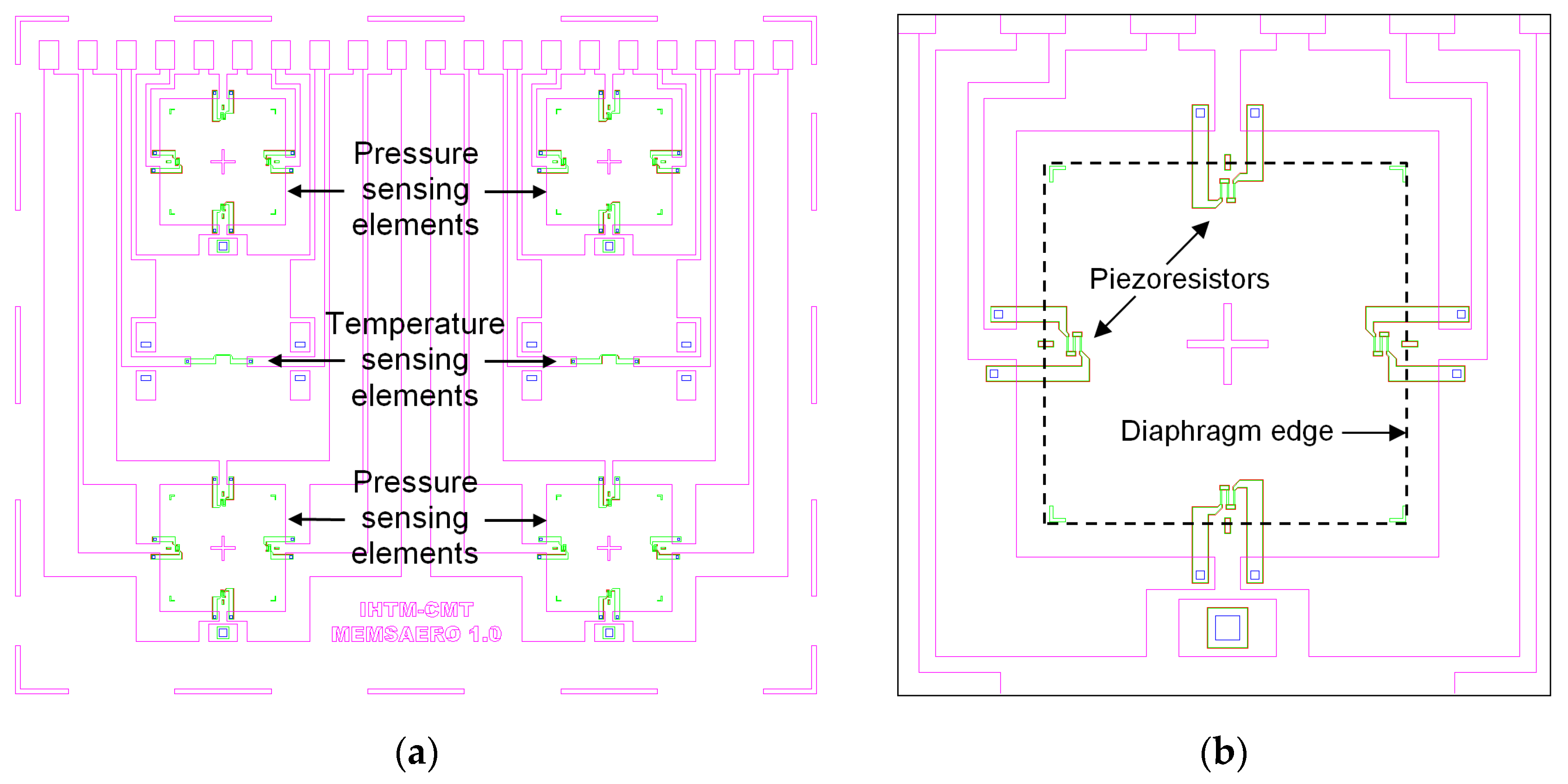
The concept of the proposed monolithically integrated multisensor structure is illustrated in Figure 1a. It is envisioned as a rectangular silicon chip with four piezoresistive MEMS pressure-sensing elements and two resistive temperature-sensing elements, as well as the necessary interconnects and wire bonding pads. The temperature-sensing elements are intended for direct temperature sensing on the chip. The thermal coupling between the temperature- and pressure-sensing elements on the same chip is much better than is possible in the case of pressure and temperature sensors on separate substrates. This is important for the temperature compensation of the pressure-sensing elements. Another important advantage of the concept is that it enables better matching of characteristics of the pressure-sensing elements on the same chip, because they are fabricated simultaneously during the same technological processes.
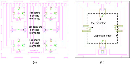
Figure 1.
Topographic image of photolithographic masks used for the multisensor chip fabrication: (a) whole chip; (b) details of a pressure-sensing element.
Silicon piezoresistive MEMS pressure sensor chips are typically fabricated on single-crystal silicon wafers with the crystallographic orientation (100). In general, a pressure-sensing element consists of a precisely defined mechanical structure (i.e., a diaphragm), and piezoresistors formed near the diaphragm’s edges, in the crystallographic direction <110>. The piezoresistors are placed at the locations where the highest mechanical stress occurs during the diaphragm deflection caused by the measured pressure. Usually, four such piezoresistors are used, of which two are in the radial direction and the remaining two in the tangential direction relative to the diaphragm which is typically quadratic in shape. The four piezoresistors form a Wheatstone bridge, so that a differential voltage signal proportional to the measured pressure value is generated when sensor excitation is applied. The structure of a pressure-sensing element is shown in more detail in Figure 1b.
2.1. Computer Simulations
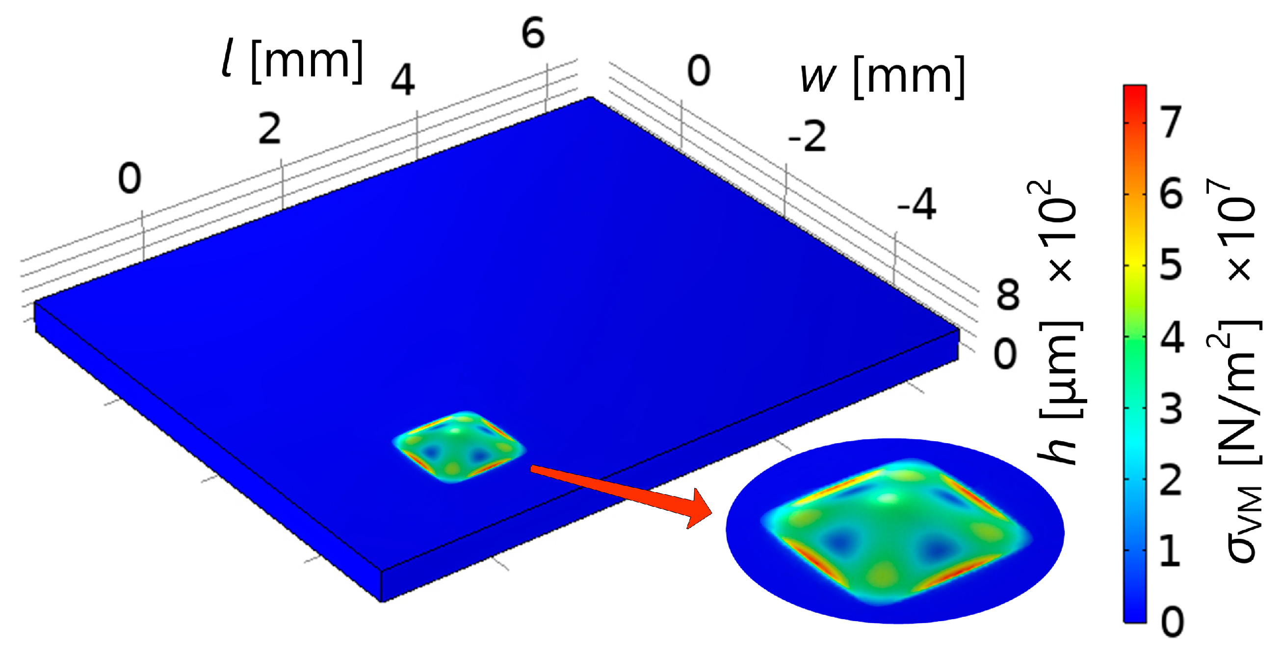
Computer simulations based on the finite element method (FEM) were performed with the main goal of investigating the parasitic influence that the mechanical stress caused by the pressure applied to one of the pressure-sensing elements may have on the other sensing elements on the same multisensor chip. In this case, the displacement profile and von Mises stress of the chip’s surface were observed, and the applied pressure was 100 kPa. The results are shown visually in Figure 2.

Figure 2.
Visual representation of the computer simulation results: the displacement of the multisensor chip’s top surface caused by the pressure of 100 kPa applied to one pressure-sensing element (in the bottom corner); color grading represents von Mises stress, according to the color scale on the right.
The simulations confirmed that the above-mentioned influence is negligible. Hence, the preliminary design of the multisensor chip was accepted. Based on it, the final design was created and subsequently used for chip fabrication.
2.2. Multisensor Chip Fabrication
The MEMS multisensor chip is developed based on ICTM’s extensive experience in the field [4,5,6], including the ICTM SP-12 pressure sensor chip intended for the measurement of medium pressures. The multisensor chip is produced using 1 μm technology. The photolithographic masks were created using the following equipment: EVG 620 double sided mask aligner (EV Group Europe & Asia/Pacific GmbH, St. Florian am Inn, Austria) and Microtech LaserWriter LW405 (MICROTECH srl, Palermo, Italy). The fabrication started with silicon wafers of the following characteristics: n-type (resistivity from 3 Ωcm to 5 Ωcm), polished on both sides, 76.2 mm (3″) in diameter, (100) orientation. The piezoresistors were formed by the diffusion of p-type impurities (boron), resulting in electrical resistance in the range from 2 kΩ to 4 kΩ. Metallic interconnects and bonding pads were formed by the deposition of aluminum (high vacuum sputtering at ≈2·10−4 Pa). The diaphragms of the pressure-sensing elements were produced by anisotropic wet chemical etching in 30% KOH water solution.
3. Results and Discussion
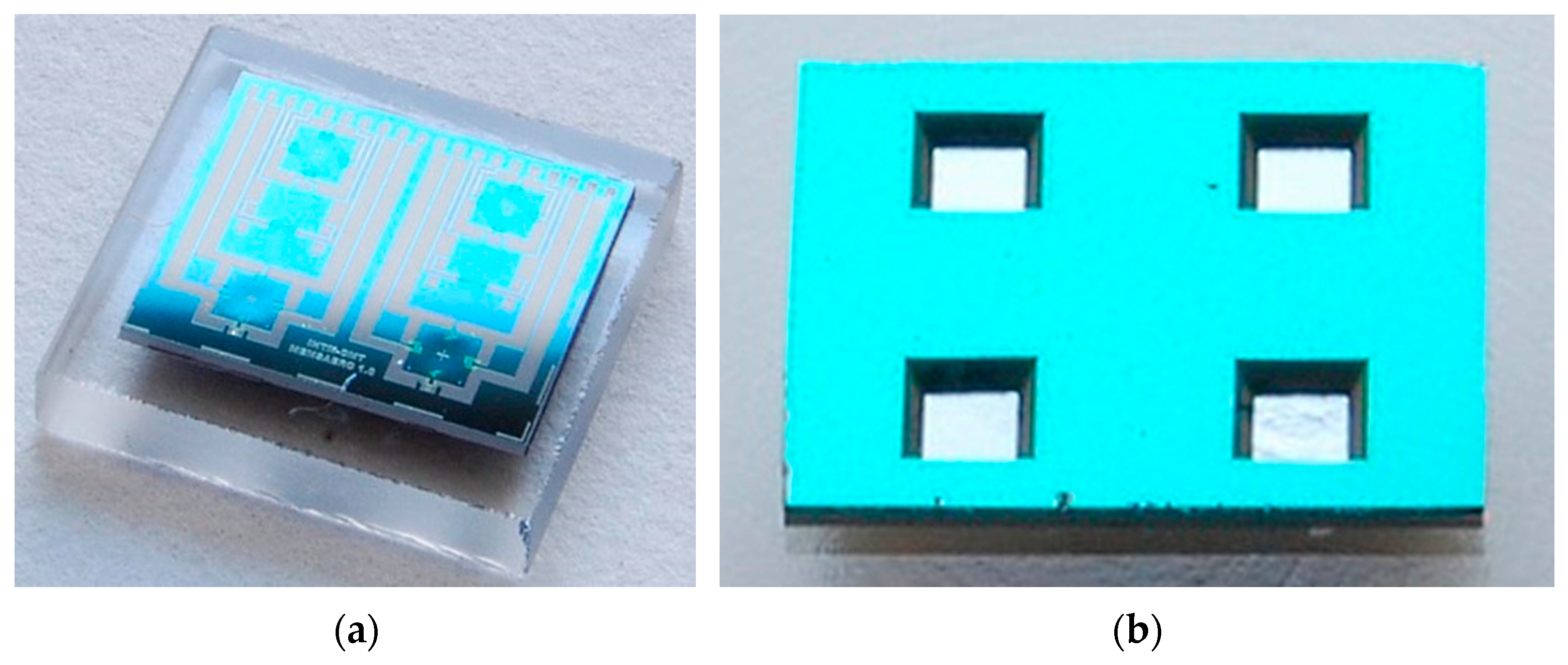
Photographs of the produced multisensor chip are shown in Figure 3. For the purposes of testing and characterization, the chip was anodically bonded to a flat Pyrex glass plate using the AML AWB-04 aligner wafer bonder (Applied Microengineering Ltd., Didcot, Oxfordshire, UK). As the bonding is performed in a vacuum, the pressure-sensing elements’ diaphragms are deflected by the atmospheric pressure, which is noticeable in Figure 3a for the lower two pressure-sensing elements. A photograph of the bottom side of the chip, showing the etched MEMS diaphragms, is shown in Figure 3b.
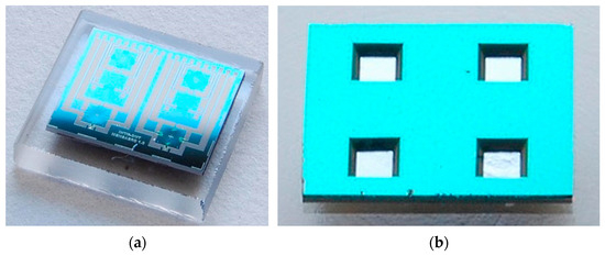
Figure 3.
Photographs of the realized MEMS multisensor chip: (a) top side; (b) bottom side (four etched MEMS diaphragms).
Three silicon wafers were processed, each with 30 chips. Electrical tests were carried out using a probing station and a semiconductor parameter analyzer.
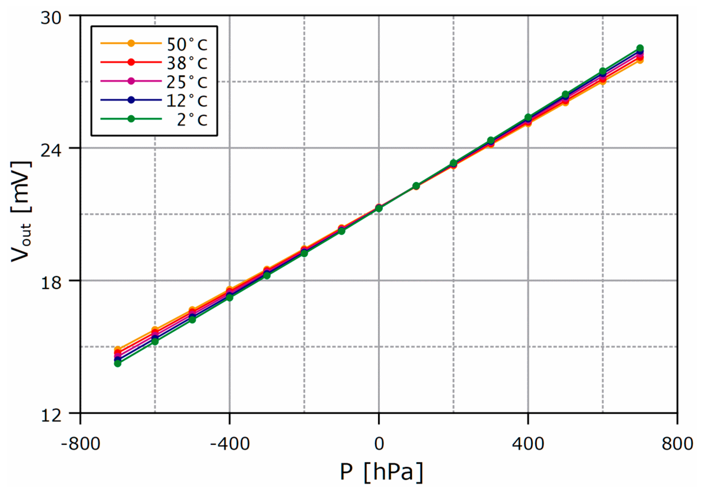
A preliminary characterization of the chip was performed by connecting the pressure-sensing elements to a constant voltage excitation of 2.5 V, and measuring their output voltages at several pressure and temperature values. The applied relative pressure was in the range from −700 hPa to 700 hPa. It was set using the Mensor APC 600 automated pressure calibrator (Mensor LP, San Marcos, Texas, USA). The temperature from 2 °C to 50 °C was set using the Heraeus Vötsch VMT 04/140 temperature chamber (Weiss Technik GmbH, Reiskirchen-Lindenstruth, Germany). The results are presented in a graph in Figure 4. They indicate that the chip performs as expected.

Figure 4.
Results of the preliminary characterization of the obtained multisensor chip: the dependence of the output voltage of a tested pressure-sensing element on the applied pressure, with temperature as a parameter.
4. Conclusions
In this paper, we presented the development of the MEMS multisensor chip intended for aerodynamic pressure measurements. We briefly explained the concept and the methodology, which included the chip design, computer simulations and, finally, the fabrication processes that resulted in the finished chip. We also performed the preliminary characterization of the chip.
The development of the multisensor chip is an important step toward the higher integration, higher performance, and further miniaturization of aerodynamic pressure measurement devices. Our future work in this field will include a detailed characterization of the developed multisensor chip, and the development of signal-processing methods in order to optimize the pressure measurement performance. Also, the possibility of increasing the number of sensing elements on the chip will be considered.
Author Contributions
Conceptualization, M.F. and Ž.L.; methodology, Ž.L., M.M.S., D.T., M.R.-R., K.C., E.M., M.V.B. and S.A.; validation, Ž.L., D.T. and P.P.; formal analysis, Ž.L. and M.F.; investigation, Ž.L., M.M.S. and D.T.; resources, M.F.; writing—original draft preparation, M.F., Ž.L. and D.T.; writing—review and editing, P.P.; visualization, Ž.L. and D.T.; supervision, M.F.; project administration, M.F.; funding acquisition, M.F. All authors have read and agreed to the published version of the manuscript.
Funding
This research was supported by the Science Fund of the Republic of Serbia, Grant Number 7754287, MEMS Multisensor Instrument for Aerodynamic Pressure Measurements—MEMSAERO. It was also supported by the Ministry of Science, Technological Development and Innovation of the Republic of Serbia, Grant Number 451-03-47/2023-01/200026.
Data Availability Statement
Data are contained within the article.
Conflicts of Interest
The authors declare no conflicts of interest. The funders had no role in the writing of the manuscript or in the decision to publish the results.
References
- Kumar, S.S.; Pant, B.D. Design principles and considerations for the ‘ideal’ silicon piezoresistive pressure sensor: A focused review. Microsyst. Technol. 2014, 20, 1213–1247. [Google Scholar] [CrossRef]
- Fiorillo, A.S.; Critello, C.D.; Pullano, S.A. Theory, technology and applications of piezoresistive sensors: A review. Sens. Actuators A 2018, 281, 156–175. [Google Scholar] [CrossRef]
- Zhang, J.; Chen, J.; Li, M.; Ge, Y.; Wang, T.; Shan, P.; Mao, X. Design, Fabrication, and Implementation of an Array-Type MEMS Piezoresistive Intelligent Pressure Sensor System. Micromachines 2018, 9, 104. [Google Scholar] [CrossRef] [PubMed]
- Djurić, Z.; Matić, M.; Matović, J.; Petrović, R.; Simičić, N. Experimental determination of silicon pressure sensor diaphragm deflection. Sens. Actuators 1990, 24, 175–179. [Google Scholar] [CrossRef]
- Simičić, N.; Tanasković, D.; Djurić, Z.; Lazić, Ž.; Petrović, R.; Matović, J.; Popović, M.; Matić, M.; Totovski, D. Investigation of impurity distribution for pressure sensor piezoresistors. J. Serb. Chem. Soc. 1993, 58, 951–957. [Google Scholar]
- Smiljanić, M.M.; Jović, V.; Lazić, Ž. Maskless convex corner compensation technique on a (1 0 0) silicon substrate in a 25 wt% TMAH water solution. J. Micromech. Microeng. 2012, 22, 115011. [Google Scholar] [CrossRef]
Disclaimer/Publisher’s Note: The statements, opinions and data contained in all publications are solely those of the individual author(s) and contributor(s) and not of MDPI and/or the editor(s). MDPI and/or the editor(s) disclaim responsibility for any injury to people or property resulting from any ideas, methods, instructions or products referred to in the content. |
© 2023 by the authors. Licensee MDPI, Basel, Switzerland. This article is an open access article distributed under the terms and conditions of the Creative Commons Attribution (CC BY) license (https://creativecommons.org/licenses/by/4.0/).