
Modeling of the Density of States in Field-Effect Zinc Oxide Semiconductor Devices Fabricated by Ultrasonic Spray Pyrolysis on Plastic Substrates †


Abstract
:1. Introduction
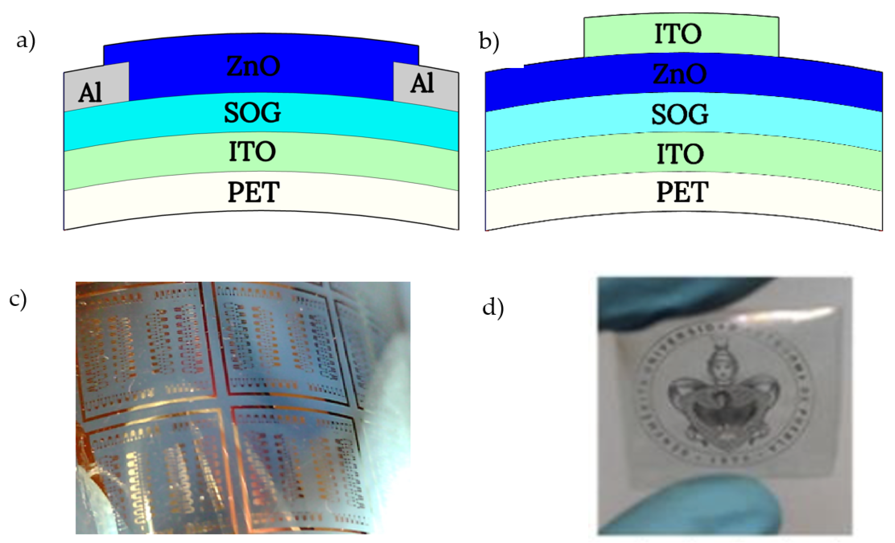
2. Experimental
3. Simulation
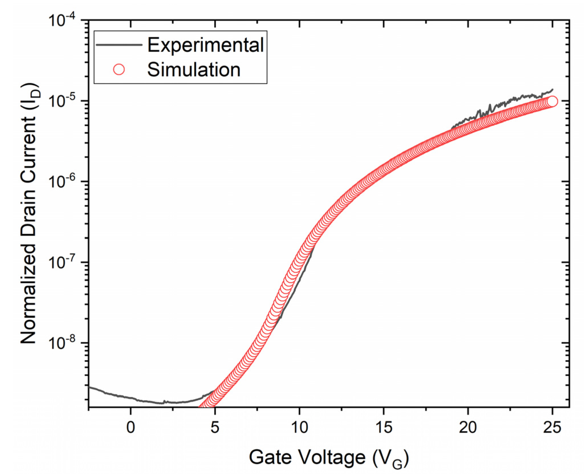
4. Results and Discussion
5. Conclusions
Funding
Data Availability Statement
Acknowledgments
Conflicts of Interest
References
- Hossain, F.M.; Nishii, J.; Takagi, S.; Ohtomo, A.; Fukumura, T.; Fujioka, H.; Kawasaki, M. Modeling and simulation of polycrystalline ZnO thin-film transistors. J. Appl. Phys. 2003, 94, 7768–7777. [Google Scholar] [CrossRef]
- Lu, N.; Jiang, W.; Wu, Q.; Geng, D.; Li, L.; Liu, M. A review for compact model of thin-film transistors (TFTs). Micromachines 2018, 9, 599. [Google Scholar] [CrossRef] [PubMed]
- Godo, H.; Kawae, D.; Yoshitomi, S.; Sasaki, T.; Ito, S.; Ohara, H.; Yamazaki, S. P-9: Numerical analysis on temperature dependence of characteristics of amorphous In-Ga-Zn-Oxide TFT. In SID Symposium Digest of Technical Papers; Blackwell Publishing Ltd.: Oxford, UK, 2009; Volume 40, pp. 1110–1112. [Google Scholar]
- Kim, D.K.; Park, J.; Zhang, X.; Park, J.; Bae, J.H. Numerical Study of Sub-Gap Density of States Dependent Electrical Characteristics in Amorphous In-Ga-Zn-O Thin-Film Transistors. Electronics 2020, 9, 1652. [Google Scholar] [CrossRef]
- Abe, K.; Ota, K.; Kuwagaki, T. Device Modeling of Oxide Semiconductor TFTs. In Proceedings of the 2020 27th International Workshop on Active-Matrix Flatpanel Displays and Devices (AM-FPD), Kyoto, Japan, 1–4 September 2020; pp. 137–140. [Google Scholar]
- Zhang, A.; Zhao, X.-R.; Duan, L.-B.; Liu, J.-M.; Zhao, J.-L. Numerical study on the dependence of ZnO thin-film transistor characteristics on grain boundary position. Chin. Phys. B 2011, 20, 57201. [Google Scholar] [CrossRef]
- Dosev, D.; Inıguez, B.; Marsal, L.F.; Pallares, J.; Ytterdal, T. Device simulations of nanocrystalline silicon thin-film transistors. Solid-State Electron. 2003, 47, 1917–1920. [Google Scholar] [CrossRef]
- Obregón, O.; Luna-Lopez, J.A.; Dominguez, M. Transistores de Película Delgada Basados en Oxido de Zinc por Spray Pyrolysis Ultrasónico de Alta Frecuencia a Baja Temperatura. Rev. Mex. Física 2021. accepted. [Google Scholar] [CrossRef]
- Park, J.H.; Lee, S.; Jeon, K.; Kim, S.; Kim, S.; Park, J.; Kim, D.H. Density of states-based DC I–V model of amorphous gallium–indium–zinc-oxide thin-film transistors. IEEE Electron Device Lett. 2009, 30, 1069–1071. [Google Scholar] [CrossRef]
- ATLAS User’s Manual; Silvaco International: Santa Clara, CA, USA, 2002.
- Chen, W.F.; Qin, G.M.; Zhou, L.; Wu, W.J.; Zou, J.H.; Xu, M.; Peng, J.B. A physics-based model of flat-band capacitance for metal oxide thin-film transistors. AIP Adv. 2018, 8, 65319. [Google Scholar] [CrossRef]
- Dominguez, M.A.; Alcantara, S.; Soto, S. Physically-based simulation of zinc oxide thin-film transistors: Contact resistance contribution on density of states. Solid-State Electron. 2016, 120, 41–46. [Google Scholar] [CrossRef]
- Dominguez, M.A.; Pau, J.L.; Redondo-Cubero, A. Unusual ambipolar behavior in zinc nitride thin-film transistors on plastic substrates. Semicond. Sci. Technol. 2019, 34, 55002. [Google Scholar] [CrossRef]
- Gupta, D.; Jang, J.; Nayak, P.K.; Hong, Y. Investigating the environmental stability of Li-doped ZnO based thin film transistors by two dimensional numerical simulations. In Proceedings of the 2010 23rd Annual Meeting of the IEEE Photonics Society, Denver, CO, USA, 7–11 November 2010; pp. 309–310. [Google Scholar]
- Saha, J.K.; Billah, M.M.; Bukke, R.N.; Kim, Y.G.; Mude, N.N.; Siddik, A.B.; Jang, J. Highly stable, nanocrystalline, ZnO thin-film transistor by spray pyrolysis using High-K dielectric. IEEE Trans. Electron Devices 2020, 67, 1021–1026. [Google Scholar] [CrossRef]
- Ditshego, N.M.; Sultan, S.M. 3D Simulation Investigating ZnO NWFET Characteristics. J. Nano Res. 2019, 58, 40–48. [Google Scholar] [CrossRef]
- Torricelli, F.; Meijboom, J.R.; Smits, E.; Tripathi, A.K.; Ferroni, M.; Federici, S.; Cantatore, E. Transport physics and device modeling of zinc oxide thin-film transistors part I: Long-channel devices. IEEE Trans. Electron Devices 2011, 58, 2610–2619. [Google Scholar] [CrossRef]
- Fung, T.C.; Chuang, C.S.; Chen, C.; Abe, K.; Cottle, R.; Townsend, M.; Kanicki, J. Two-dimensional numerical simulation of radio frequency sputter amorphous In–Ga–Zn–O thin-film transistors. J. Appl. Phys. 2009, 106, 84511. [Google Scholar] [CrossRef]
- Dominguez, M.; Rosales, P.; Torres, A.; Moreno, M.; Molina, J.; De la Hidalga, F.; Calleja, W. Ambipolar a-SiGe: H thin-film transistors fabricated at 200° C. J. Non-Cryst. Solids 2012, 358, 2340–2343. [Google Scholar] [CrossRef]
- Park, J.H.; Jeon, K.; Lee, S.; Kim, S.; Kim, S.; Song, I.; Kim, D.H. Extraction of density of states in amorphous GaInZnO thin-film transistors by combining an optical charge pumping and capacitance–voltage characteristics. IEEE Electron Device Lett. 2008, 29, 1292–1295. [Google Scholar] [CrossRef]
- Jeon, K.; Kim, C.; Song, I.; Park, J.; Kim, S.; Kim, S.; Kim, D.H. Modeling of amorphous InGaZnO thin-film transistors based on the density of states extracted from the optical response of capacitance-voltage characteristics. Appl. Phys. Lett. 2008, 93, 182102. [Google Scholar] [CrossRef]


| Parameters | ZnO | Description |
|---|---|---|
| Eg (eV) | 3.05 | Energy gap |
| NTA (cm−3eV−1) | 3.5 × 10²⁰ | Density of tail-acceptor states |
| NTD (cm−3eV−1) | 4.0 × 10²⁰ | Density of tail-donor states |
| WTD (eV) | 0.05 | Decay energy of tail-donor states |
| WTA (eV) | 0.025 | Decay energy of tail-acceptor states |
| NGA (cm−3eV−1) | 1.0 × 10¹⁷ | Density of deep-acceptor states |
| NGD (cm−3eV−1) | 1.5 × 10¹⁹ | Density of deep-donor states |
| WGD (eV) | 0.1 | Decay energy of deep-donor states |
| WGA (eV) | 0.05 | Decay energy of deep-acceptor states |
| EGD (eV) | 0.1 | Peak energy of deep-donor states |
| EGA (eV) | 0.35 | Peak energy of deep-acceptor states |
| (cm2/Vs) | 15 | Electron band mobility |
| (cm2/Vs) | 0.1 | Hole band mobility |
Publisher’s Note: MDPI stays neutral with regard to jurisdictional claims in published maps and institutional affiliations. |
© 2021 by the authors. Licensee MDPI, Basel, Switzerland. This article is an open access article distributed under the terms and conditions of the Creative Commons Attribution (CC BY) license (https://creativecommons.org/licenses/by/4.0/).
Share and Cite
Obregon, O.; Barba, D.; Dominguez, M.A. Modeling of the Density of States in Field-Effect Zinc Oxide Semiconductor Devices Fabricated by Ultrasonic Spray Pyrolysis on Plastic Substrates. Eng. Proc. 2021, 4, 12. https://doi.org/10.3390/Micromachines2021-09552
Obregon O, Barba D, Dominguez MA. Modeling of the Density of States in Field-Effect Zinc Oxide Semiconductor Devices Fabricated by Ultrasonic Spray Pyrolysis on Plastic Substrates. Engineering Proceedings. 2021; 4(1):12. https://doi.org/10.3390/Micromachines2021-09552
Chicago/Turabian StyleObregon, Ovier, David Barba, and Miguel A. Dominguez. 2021. "Modeling of the Density of States in Field-Effect Zinc Oxide Semiconductor Devices Fabricated by Ultrasonic Spray Pyrolysis on Plastic Substrates" Engineering Proceedings 4, no. 1: 12. https://doi.org/10.3390/Micromachines2021-09552
APA StyleObregon, O., Barba, D., & Dominguez, M. A. (2021). Modeling of the Density of States in Field-Effect Zinc Oxide Semiconductor Devices Fabricated by Ultrasonic Spray Pyrolysis on Plastic Substrates. Engineering Proceedings, 4(1), 12. https://doi.org/10.3390/Micromachines2021-09552