Transfer Printing of Conductive Thin Films on PDMS with Soluble Substrates for Flexible Biosensors †

Abstract
:1. Introduction
2. Methods
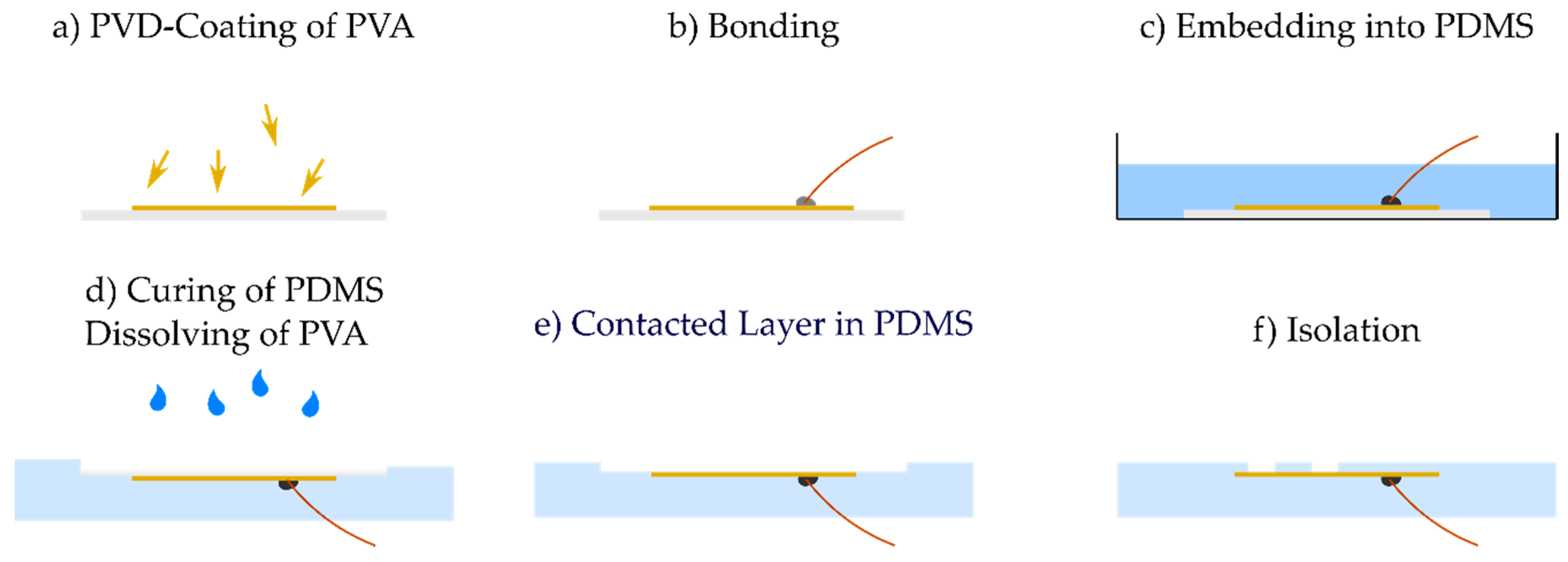
2.1. Fabrication
2.2. Adhesion
2.3. Conductivity
2.4. Flexibility
2.5. Impedance Measurement
2.6. Demonstrator
2.7. Adaptivity
3. Results and Discussion
3.1. Adhesion
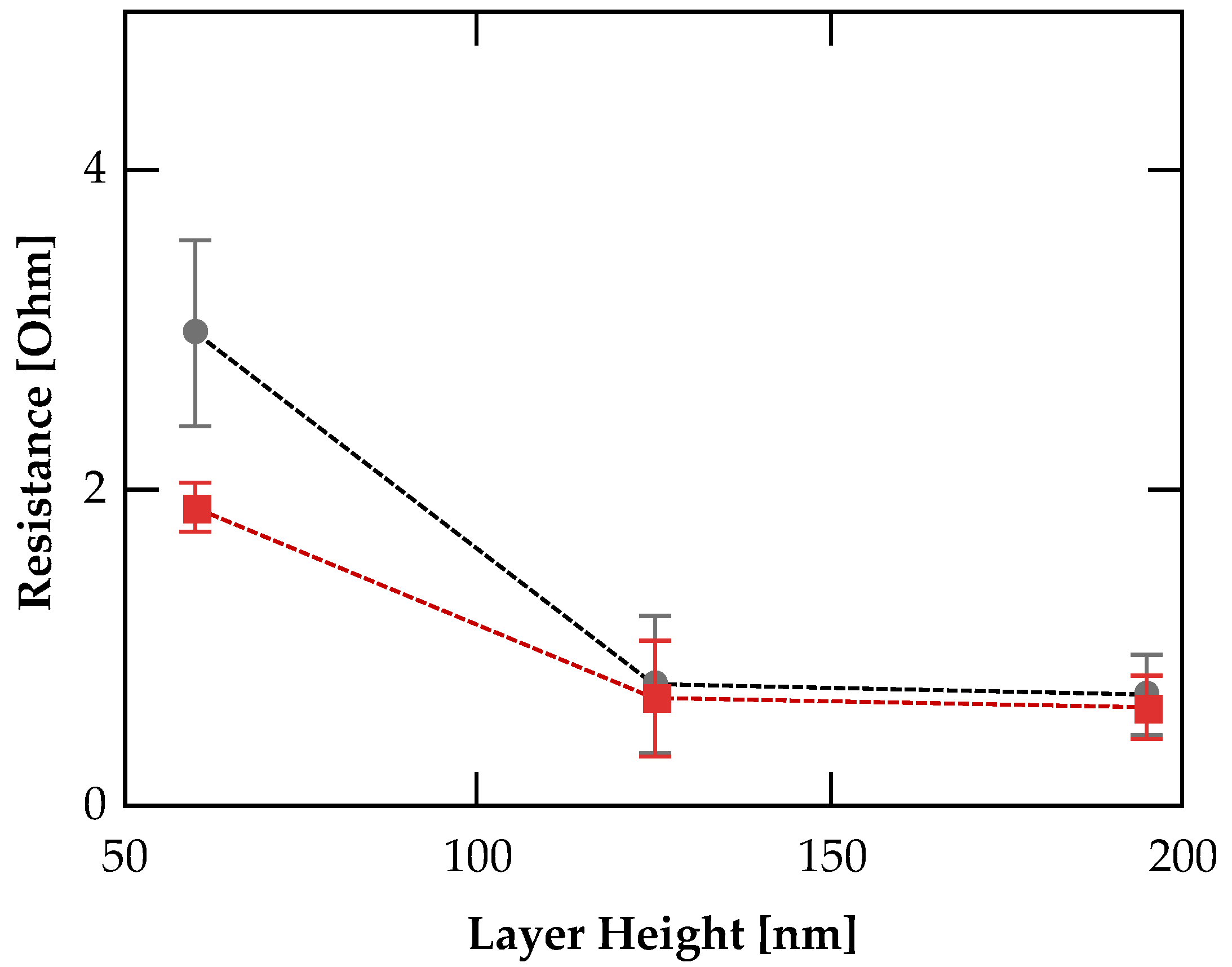
3.2. Conductivity
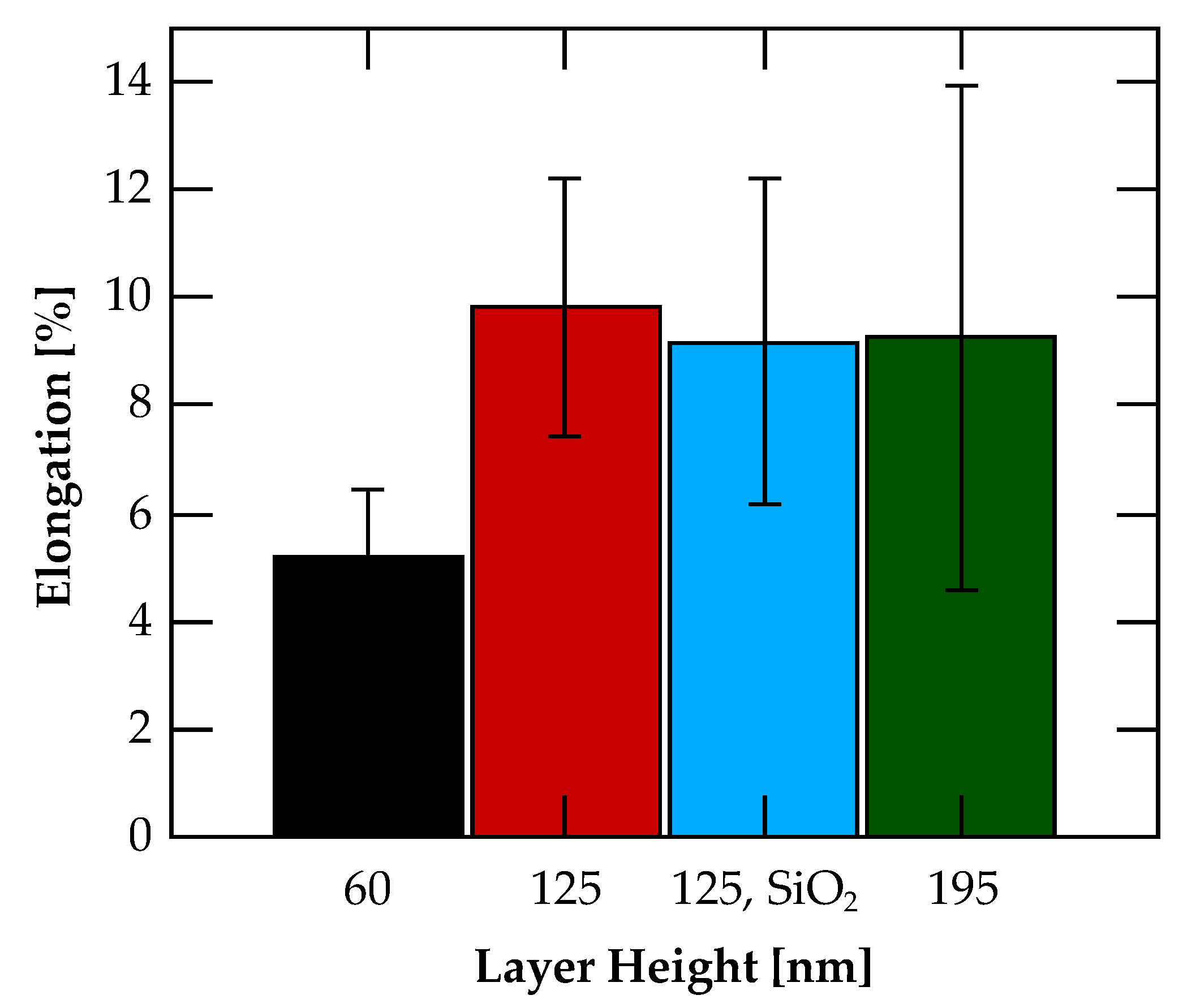
3.3. Flexibility
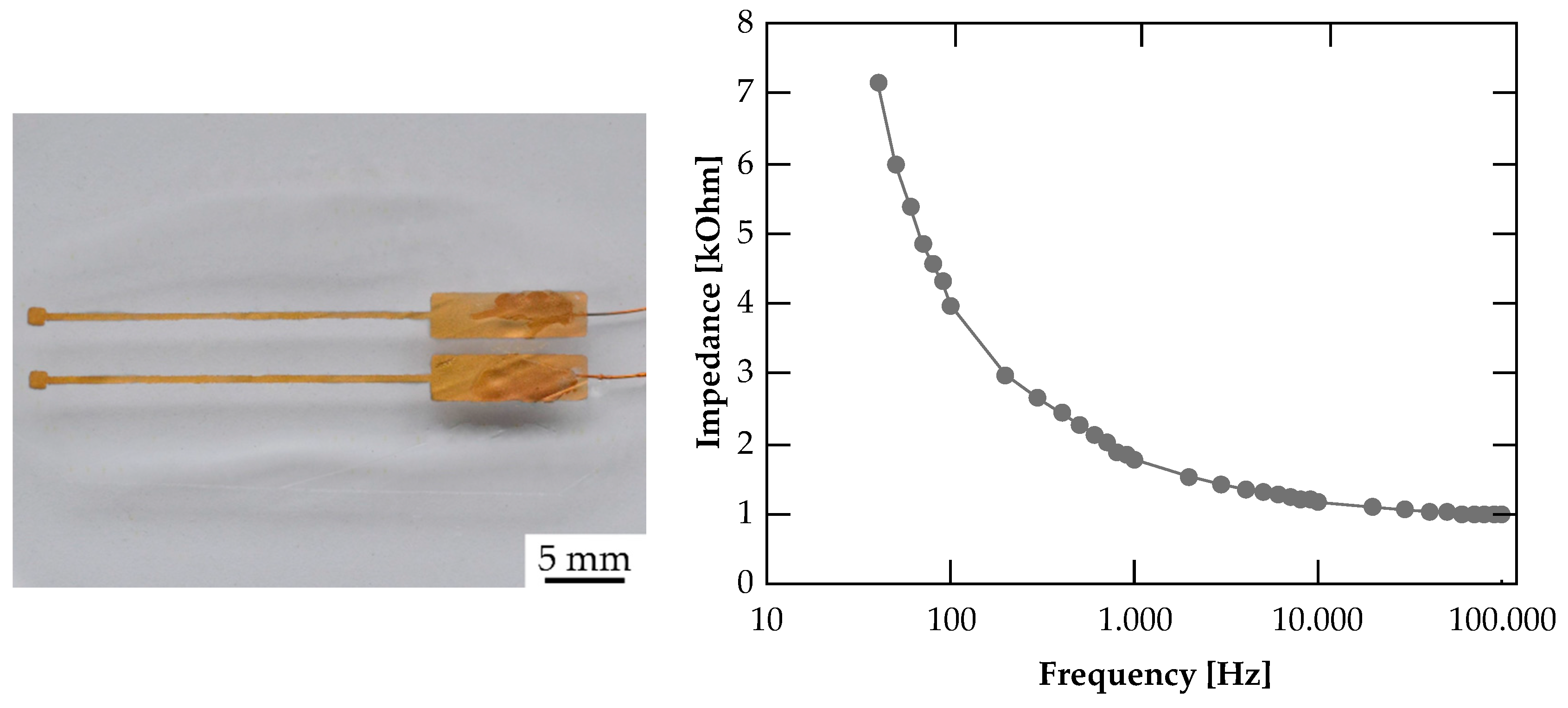
3.4. Impedance Measurement
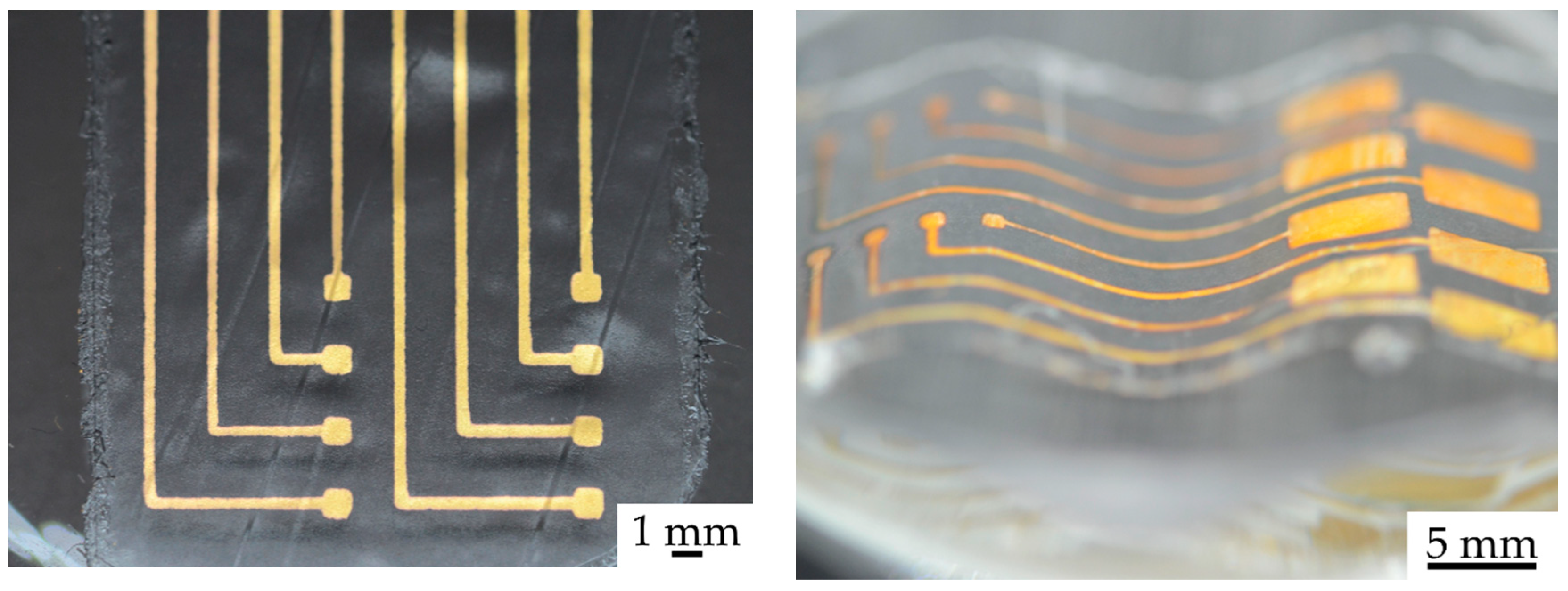
3.5. Demonstrator
3.6. Adaptivity
4. Conclusions
Author Contributions
Funding
Conflicts of Interest
References
- Baura, G.D. Medical Device Technologies: A Systems Based Overview Using Engineering Standards; Elsevier: Amsterdam, The Netherlands; Academic Press: Amsterdam, Waltham, MA, USA, 2012; ISBN 9780123749765. [Google Scholar]
- Allison, B.Z.; Dunne, S.; Leeb, R.; Del R. Millán, J.; Nijholt, A. Towards Practical Brain-Computer Interfaces. Bridging the Gap from Research to Real-World Applications; Springer: Berlin/Heidelberg, Germany, 2013; ISBN 978-3-642-29745-8. [Google Scholar]
- Ball, T.; Kern, M.; Mutschler, I.; Aertsen, A.; Schulze-Bonhage, A. Signal quality of simultaneously recorded invasive and non-invasive EEG. NeuroImage 2009, 46, 708–716. [Google Scholar] [CrossRef] [PubMed]
- Rubehn, B.; Bosman, C.; Oostenveld, R.; Fries, P.; Stieglitz, T. A MEMS-based flexible multichannel ECoG-electrode array. J. Neural Eng. 2009, 6, 36003. [Google Scholar] [CrossRef] [PubMed]
- Kim, D.-H.; Viventi, J.; Amsden, J.J.; Xiao, J.; Vigeland, L.; Kim, Y.-S.; Blanco, J.A.; Panilaitis, B.; Frechette, E.S.; Contreras, D.; et al. Dissolvable films of silk fibroin for ultrathin conformal bio-integrated electronics. Nat. Mater. 2010, 9, 511–517. [Google Scholar] [CrossRef] [PubMed]
- Tolstosheeva, E.; Gordillo-González, V.; Biefeld, V.; Kempen, L.; Mandon, S.; Kreiter, A.K.; Lang, W. A multi-channel, flex-rigid ECoG microelectrode array for visual cortical interfacing. Sensors 2015, 15, 832–854. [Google Scholar] [CrossRef] [PubMed]
- Takahashi, H.; Ejiri, T.; Nakao, M.; Nakamura, N.; Kaga, K.; Hervé, T. Microelectrode array on folding polyimide ribbon for epidural mapping of functional evoked potentials. IEEE Trans. Biomed. Eng. 2003, 50, 510–516. [Google Scholar] [CrossRef] [PubMed]
- Rousche, P.J.; Pellinen, D.S.; Pivin, D.P.; Williams, J.C.; Vetter, R.J.; Kipke, D.R. Flexible polyimide-based intracortical electrode arrays with bioactive capability. IEEE Trans. Biomed. Eng. 2001, 48, 361–371. [Google Scholar] [CrossRef] [PubMed]
- Morris, S.; Hirata, M.; Sugata, H.; Goto, T.; Matsushita, K.; Yanagisawa, T.; Saitoh, Y.; Kishima, H.; Yoshimine, T. Patient-specific cortical electrodes for sulcal and gyral implantation. IEEE Trans. Biomed. Eng. 2015, 62, 1034–1041. [Google Scholar] [CrossRef] [PubMed]
- Larmagnac, A.; Eggenberger, S.; Janossy, H.; Vörös, J. Stretchable electronics based on Ag-PDMS composites. Sci. Rep. 2014, 4, 7254. [Google Scholar] [CrossRef] [PubMed]
- Stieghorst, J.; Tran, B.N.; Hadeler, S.; Beckmann, D.; Doll, T. Hydrogel-Based Actuation for Modiolar Hugging Cochlear Implant Electrode Arrays. Procedia Eng. 2016, 168, 1529–1532. [Google Scholar] [CrossRef]
- Nahvi, M.S.; Boroumand, F.A.; Maghami, M.H.; Sodagar, A.M.; Shojaei, A.; Mirnajafi-Zadeh, J. Design, fabrication, and test of flexible thin-film microelectrode arrays for neural interfaces. In Proceedings of the 2017 IEEE 30th Canadian Conference on Electrical and Computer Engineering (CCECE), Windsor, ON, Canada, 30 April–3 May 2017; pp. 1–4. [Google Scholar]
- Yan, Z.; Pan, T.; Xue, M.; Chen, C.; Cui, Y.; Yao, G.; Huang, L.; Liao, F.; Jing, W.; Zhang, H.; et al. Thermal Release Transfer Printing for Stretchable Conformal Bioelectronics. Adv. Sci. 2017, 4, 1700251. [Google Scholar] [CrossRef] [PubMed]


Publisher’s Note: MDPI stays neutral with regard to jurisdictional claims in published maps and institutional affiliations. |
© 2020 by the authors. Licensee MDPI, Basel, Switzerland. This article is an open access article distributed under the terms and conditions of the Creative Commons Attribution (CC BY) license (https://creativecommons.org/licenses/by/4.0/).
Share and Cite
Hadeler, S.; Bengsch, S.; Prediger, M.S.; Wurz, M.C. Transfer Printing of Conductive Thin Films on PDMS with Soluble Substrates for Flexible Biosensors. Eng. Proc. 2020, 2, 47. https://doi.org/10.3390/ecsa-7-08181
Hadeler S, Bengsch S, Prediger MS, Wurz MC. Transfer Printing of Conductive Thin Films on PDMS with Soluble Substrates for Flexible Biosensors. Engineering Proceedings. 2020; 2(1):47. https://doi.org/10.3390/ecsa-7-08181
Chicago/Turabian StyleHadeler, Steffen, Sebastian Bengsch, Maren S. Prediger, and Marc Christopher Wurz. 2020. "Transfer Printing of Conductive Thin Films on PDMS with Soluble Substrates for Flexible Biosensors" Engineering Proceedings 2, no. 1: 47. https://doi.org/10.3390/ecsa-7-08181
APA StyleHadeler, S., Bengsch, S., Prediger, M. S., & Wurz, M. C. (2020). Transfer Printing of Conductive Thin Films on PDMS with Soluble Substrates for Flexible Biosensors. Engineering Proceedings, 2(1), 47. https://doi.org/10.3390/ecsa-7-08181