Proceeding Paper

A Complementary Reduced Graphene Oxide-Based Inverter for Ion Sensing †

ITODYS, Université Paris Cité, CNRS, F-75006 Paris, France
*
Authors to whom correspondence should be addressed.
Presented at the 2nd International Electronic Conference on Biosensors, 14–18 February 2022; Available online: https://sciforum.net/event/IECB2022.
Eng. Proc. 2022, 16(1), 2; https://doi.org/10.3390/IECB2022-12272
Published: 14 February 2022
(This article belongs to the Proceedings of The 2nd International Electronic Conference on Biosensors)

Abstract

:
Graphene, a 2D material with high conductivity and stability in aqueous media, could complement silicon as raw material for sensing with transistor-based devices in liquids. Furthermore, the fabrication of graphene-based transistors is affordable with low-cost techniques such as inkjet printing from graphene oxide (GO)-based inks. Deposited on plastic conformable substrates, graphene-based logic gates are standing as favorable and compelling candidates in the field of biosensing, to make electrical transduction and binary operations match with aqueous media and facilitate diagnostic operations.

1. Introduction

Graphene-based transistors are well known for being ambipolar devices stable in aqueous media, with high channel conductivity and charge carrier mobility, in comparison with organic semiconductor-based ones [1]. Electrolyte-gated graphene-based field-effect transistors (EG-GFETs) are composed of three electrodes, named source, drain, and gate, as in the case of conventional FETs, but they possess a few specificities of their own [2]. First of all, graphene cannot be considered as a semiconductor regarding its electrical behavior; in addition to that, the electrolyte separating the gate from the transistor’s channel is easily tunable and modifiable, and that stands for both dielectric and sensing medium [3]. This latter property is particularly remarkable as the nature of the electrolyte induces a change in the electrochemical double-layer capacitance at the gate–electrolyte and graphene–electrolyte interfaces, which, in turn, leads to a modification of the electrical properties of the transistor itself [4]. The use of graphene transistors as biological or ionic sensors has already been highly reported [5]; however, logic gates built from graphene transistors have never been described for such purpose, even though few articles are already revealing research interest in such devices to perform basic logic operations in aqueous media [6]. In this study, we investigate the design of a logic gate for ion-sensing purposes from graphene-based electrical devices on flexible substrates, to further extend the application field to skin patches or bandage-type sensors, for instance.

2. Materials and Method

Transistors were designed with a coplanar gate configuration (Figure 1, left). The fabrication steps, from electrode patterning by photolithography to the electrochemical reduction of the GO ink-coated channel by drop-casting or inkjet printing method, are described elsewhere [7]. All electrolytes used were DI-water-based solutions, containing K+ and/or Na+ at various concentrations. Valinomycin (VMC) ion-selective membrane, specific to K+, was deposited on the gate of each transistor by using the KELENN DMD100 printer. The composition was adapted from the method of Kisiel et al. [8] as follows: 1.0% (w/w) of valinomycin; 0.5% of potassium tetrakis [3,5-bis(trifluoromethyl) phenyl]borate (KTBP) selectophore to improve VMC selectivity; 31.5% of poly (vinyl chloride) polymer and 67.0% of 2-nitrophenyl octyl ether plasticizer in cyclohexanone instead of THF as a solvent to prevent fast evaporation in the dispenser syringe. The conventional silicon wafer playing the role of the substrate was replaced here by a flexible polymer foil of polyimide to match with on-skin patch application perspectives. A commercial silver ink (purchased from PV Nano Cell) allowed the interconnections between the transistors. All electrical measurements were performed with a 4200-A-SCS Keithley analyzer. The biased supply voltage to acquire inverter characteristics was applied through an external power source (Basetech BT-305 DC).

3. Results and Discussion

3.1. Electrical Characteristics of the EG-GFET Inverter

Regarding the ambipolar behavior of rGO, one expects an increase in drain current IDS, apart from a minimum value that occurs at VGS = V0, corresponding to the situation where the Fermi level crosses the so-called Dirac point [1]. The electrochemical reduction of GO to rGO was controlled by measuring the amount of charge passed at a constant reduction voltage, showing good control of the V0 = VGS (at IDS,min). V0 can be tuned as shown in Figure 1, right; the higher the amount of charge, the less positive the value of V0. However, even with a significant value of charge injected, V0 stays positive, which indicates that the rGO built following this process is still p-doped [5,7].
The difference in V0 from one to another transistor may be caused by a difference in the doping state. Therefore, a slight shift of a few tens of mV is enough to build an inverter out of two graphene transistors made from two different reduction charges: The two gates, as well as the drains, were connected together so that the transistor with the highest V0 acted as the p transistor and connected to VDD from its source; the second one, still p-doped even if less, was connected to the ground and acted as the n transistor of a usual NOT gate. The electrical characteristic of the resulting gate is shown in Figure 2.

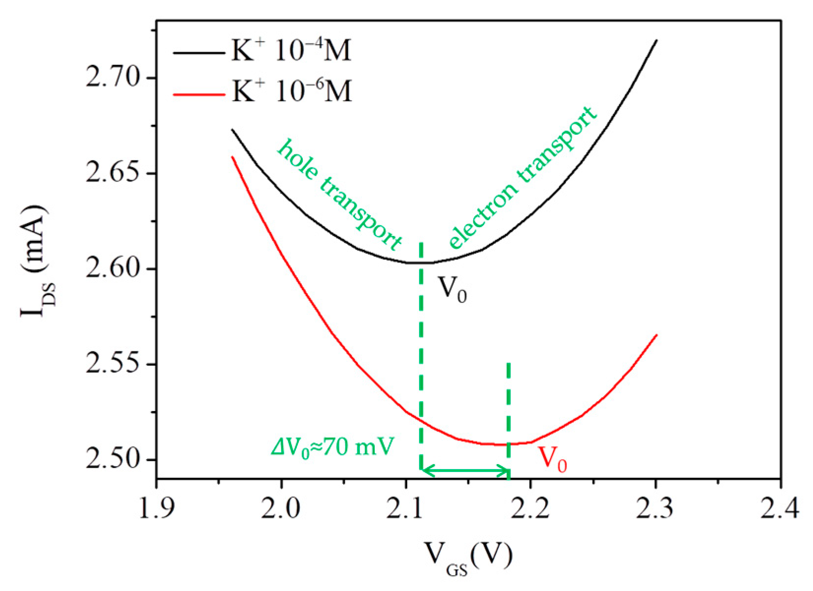
3.2. The EG-GFET Inverter as K+ Sensor

One way to study inverters is to consider each of the transistors T1 and T2 as a variable resistor. The competition between those two connected transistors is related to the ratio RT1 versus RT2: when the upper transistor, connected to the biased supply voltage VDD, is driving the device, i.e., RT1 < RT2 occurring for low input VIN, the output is connected to the supply voltage corresponding to the ON state. On the other hand, when RT2 < RT1, the bottom transistor connects the ground to the output resulting in the OFF state.
It is clearly evident from above that different reduction levels lead to a shift in the V0 of the two transistors; however, this shift can also be obtained by changing the capacitance at the gate–electrolyte interface, which is the way that we investigated in order to build a proper sensor out of the rGO inverter.
Functionalization of the gate electrode with ionophores or other specific hydrogel modifies the capacitance at the gate–electrolyte interface that induces a change in the effective gate voltage at the input of the modified transistor.
Figure 3 gives an example of ion sensing with rGO transistors, as the transfer characteristic is directly impacted by a change in the concentration of K+ ions of the electrolyte, from 10−6 to 10−4 M, with a VMC gate-modified transistor.
We plan to use the rGO-based inverters to assist ion sensing, following the above-mentioned principle, which consists of performing the switch from OFF state to ON state, for a fixed VIN, owing to the capacitance changes occurring at the gate–electrolyte interface of one of the two transistors, resulting in a change in the V0 value. In this configuration, the ion concentration involved in the capacitance change is standing for the input information of the sensor. The main interest of sensing with inverters instead of isolated transistors is to take advantage of the Boolean algebra applied to graphene logic gates, which could allow us to design complex circuits stable in aqueous media and thus to perform chemical logic, which is an ingenious method to produce basic mathematical operations in solution, or, more concretely, to obtain a unique sensor built from the output responses of several ones in the same medium.

4. Conclusions

In this study, we reported a way to perform ion sensing with the most elementary logic gate—the inverter—from two interconnected transistors. To overcome heavy and costly processes of graphene deposition, we formulated a graphene oxide surfactant-free ink that can be directly inkjet printed on the channel. As an ongoing study, we are currently investigating the way to make the inverter switch occur, thereby estimating the sufficient threshold value of capacitance or ion concentration change needed to change from OFF to ON output state, through both experimental work and simulation.

Author Contributions

Conceptualization, G.M., N.B. and B.P.; methodology, R.B., G.M., N.B. and B.P.; investigation, R.B.; writing, R.B., G.M., N.B. and B.P.; supervision, G.M., N.B. and B.P. All authors have read and agreed to the published version of the manuscript.

Funding

This research received funding from the Consortium of French higher education and research institutions for the development of USTH, under the framework “Collaborative S&T projects 2021”, USTH.AMSN.01/21-23, entitled “Functionalized Graphene for Electrolyte-Gated Field-Effect Transistors. Application to Wearable Sweat Sensors”.

Institutional Review Board Statement

Not applicable.

Informed Consent Statement

Not applicable.

Acknowledgments

R.B thanks Ecole Doctorale ED388 Chimie Physique et Chimie Analytique de Paris Centre for providing a PhD grant.

Conflicts of Interest

The authors declare no conflict of interest.

References

  1. Hess, L.H.; Seifert, M.; Garrido, J.A. Graphene Transistors for Bioelectronics. Proc. IEEE 2013, 101, 1780–1792. [Google Scholar] [CrossRef] [Green Version]
  2. Ohno, Y.; Maehashi, K.; Yamashiro, Y.; Matsumoto, K. Electrolyte-Gated Graphene Field-Effect Transistors for Detecting pH and Protein Adsorption. Nano Lett. 2009, 9, 3318–3322. [Google Scholar] [CrossRef] [PubMed]
  3. Kireev, D.; Brambach, M.; Seyock, S.; Maybeck, V.; Fu, W.; Wolfrum, B.; Offenhäusser, A. Graphene transistors for interfacing with cells: Towards a deeper understanding of liquid gating and sensitivity. Sci. Rep. 2017, 7, 6658. [Google Scholar] [CrossRef] [PubMed]
  4. Heller, I.; Chatoor, S.; Mannik, J.; Zevenbergen, M.A.; Dekker, C.; Lemay, S.G. Influence of Electrolyte Composition on Liquid-Gated Carbon Nanotube and Graphene Transistors. J. Am. Chem. Soc. 2010, 132, 17149–17156. [Google Scholar] [CrossRef] [PubMed]
  5. Furlan de Oliveira, R.; Livio, P.A.; Montes-García, V.; Ippolito, S.; Eredia, M.; Fanjul-Bolado, P.; Gonzalez Garcia, M.B.; Casalini, S.; Samorì, P. Liquid-Gated Transistors Based on Reduced Graphene Oxide for Flexible and Wearable Electronics. Adv. Funct. Mater. 2019, 29, 1905375. [Google Scholar] [CrossRef] [Green Version]
  6. Son, M.; Kim, H.; Jang, J.; Kim, S.Y.; Ki, H.C.; Lee, B.H.; Kim, I.S.; Ham, M.H. Low-Power Complementary Logic Circuit Using Polymer-Electrolyte-Gated Graphene Switching Devices. ACS Appl. Mater. Interfaces 2019, 11, 47247–47252. [Google Scholar] [CrossRef] [PubMed]
  7. Vasilijević, S.; Mattana, G.; Anquetin, G.; Battaglini, N.; Piro, B. Electrochemical tuning of reduced graphene oxide in printed electrolyte-gated transistors. Impact on charge transport properties. Electrochim. Acta 2021, 371, 137819. [Google Scholar] [CrossRef]
  8. Kisiel, A.; Kałuża, D.; Paterczyk, B.; Maksymiuk, K.; Michalska, A. Quantifying plasticizer leakage from ion-selective membranes—A nanosponge approach. Analyst 2020, 145, 2966–2974. [Google Scholar] [CrossRef] [PubMed]
Figure 1. Coplanar gate configuration (left) and transfer characteristics for different charges during the electrochemical reduction process (right).
Engproc 16 00002 g001
Figure 2. Graphene-based inverter input (IN) versus output (OUT) characteristic. Inset: electrical circuit with T1 (p-type, slightly reduced) and T2 transistors (“n-type-like”, more reduced; see text for explanation).
Engproc 16 00002 g002
Figure 3. Transfer characteristic of VMC-modified rGO-EGFET for two different concentrations of K+ ion.
Engproc 16 00002 g003
Publisher’s Note: MDPI stays neutral with regard to jurisdictional claims in published maps and institutional affiliations.

