Abstract
Technological advancements in solar power systems necessitate highly reliable power inverters with a high efficiency and a small size. An LLC resonant converter-based pseudo Direct Current (DC) link inverters offer these qualities to some extent. The resonant circuits of conventional pseudo DC link inverters lack the ability to attain a zero gain and cannot handle variable frequency control which in turn requires very large filters to produce pure sinusoidal output voltages for grid. The usage of these filters consequences in the enhanced price and size of inverters; moreover, the reliability of inverters is also reduced. We propose a novel topology for a pseudo DC link inverter based on an LLCLC resonant converter. The proposed inverter does not require large filters, because it generates rectified sinusoidal output voltages. An additional parallel LC component is added in series to the resonant circuit, which makes it able to attain a zero gain through an infinite circuit impedance. The 400 W pseudo DC link inverter with a 40 V input and a 400 V output is designed and simulated on OrCAD PSpice software. The results showed that there is a significant improvement in achieving a zero gain. The possible lowest gain achieved is approximately 0.125. The proposed technique attested to be more efficient than those formerly used, subsequently contributing satisfying outcomes.
1. Background
The depletion of fossil fuels has triggered solar panels to become popular in producing electrical energy for over years [1]. Smaller household-size solar panels have been increasing in recent years [2]. The microinverters are excellent choices for these systems, as only one solar panel is connected to each inverter. Microinverters provide benefits of having small size, high efficiency and high reliability [3]. The output voltage of solar power plants needs to be amplified for home appliances. The pseudo Direct Current link inverter is a type of microinverter comprised of two stages. The DC–DC stage converts a DC input voltage to a rectified Alternating Current (AC) voltage which is then unfolded in the DC–AC stage. The pseudo DC link inverters are promising, because a suitable DC–DC stage can provide all the require qualities [4].
In the literature, a large amount of DC–DC converters are presented. The reliability and high efficiency of inverters can be achieved through soft switching techniques. The resonant converter provides excellent efficiency using soft switching operations [5]. LLC resonant converter-based inverters working on pulse density modulation produces pure sinusoidal outputs, but large output filters further reduce reliability and size issues [6]. LLC resonant converters require very high switching frequencies to achieve a zero tank gain, which is practically not possible [7]. The four element resonant converters provide two peak values in voltage gain, but achieving a zero gain is still not possible [8]. In contrast, LLCLC resonant converters have the ability to achieve an approximately zero gain at an achievable switching frequency [9,10,11]. The LLCLC converters consist of LLC resonant components with an additional parallel LC component in series on the primary side. The zero gain property through the additional LC component is helpful in the DC–DC stage for complete variable frequency control without using a large filter on the output side.
2. Proposed Topology
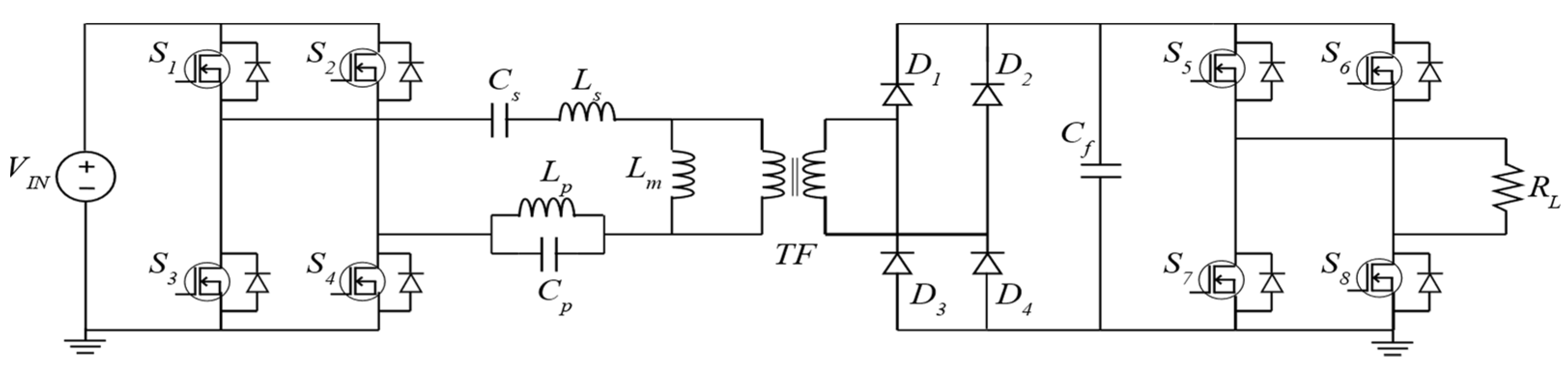
In this paper, a novel LLCLC resonant converter-based pseudo DC link inverter is proposed. The circuit of the proposed inverter is given in Figure 1. The DC–DC stage consists of a full-bridge inverter comprised of four switches (S1 to S4). The full-bridge inverter converts an input DC voltage to a square-wave voltage, which is fed to an LLCLC resonant tank of which the gain changes by inputting a square-wave frequency variation. The tank is connected to a high-frequency transformer, which can be used for the buck-boost operation and isolation purpose. The transformer is further connected to a full-wave rectifier for the rectification of the transformer output. The DC–AC stage unfolds the input-rectified voltage to an output sinusoidal voltage by using another full-bridge inverter consisting of four switches (S5 to S8).

Figure 1.
Proposed pseudo Direct Current (DC) link inverter.
The resonant tank circuit of the proposed inverter consists of five elements, i.e., Cs, Cp, Ls, Lp and Lm. Cs and Ls are series components, while Cp and Lp are parallel components. Lm provides a magnetizing inductance for the transformer. The addition of Cp and Lp changes the gain characteristics of the resonant tank, helping to achieve a zero gain. The resonant tank has three main resonant frequencies, i.e., fR1, fR2 and fR3 for different Q points. The gain is one at fR1. Below fR1, the gain is more than one to perform boost operation. Between fR1 and fR2, the gain is less than one to perform buck operation. The impedance of the resonant tank increases to infinity at fR2, providing a zero gain. At fR3, the gain is again one and has a low impedance for third harmonics, reducing reactive power. The gain G of the resonant tank with inductance ratio L, quality factor Q and normalized switching frequency fN is given by [10]:
The resonant frequencies of the LLCLC resonant tank are given as , and where and .
In the working principle of the proposed inverter, the output AC voltage cycle is divided into four stages. In stage 1, the switching frequencies of S1 and S4 change from fR2 to fR1, regulating the tank gain from zero to one. The voltage at the DC link stage continuously changes from zero to the peak amplitude value. Switches S5 and S8 are in the state ON, so the output of the inverter is the DC link voltage. In stage 2, the switching frequency changes from fR1 to fR2, regulating gain from one to zero. Similarly, the DC link voltage changes from the peak amplitude value to zero. Switches S5 and S8 are still in the state ON, thus generating the DC link voltage on the output side. In stages 3 and 4, only switches S5 and S8 are in the state OFF, while S6 and S7 are in the state ON and other processes remain the same as in earlier stages.
3. Design Consideration
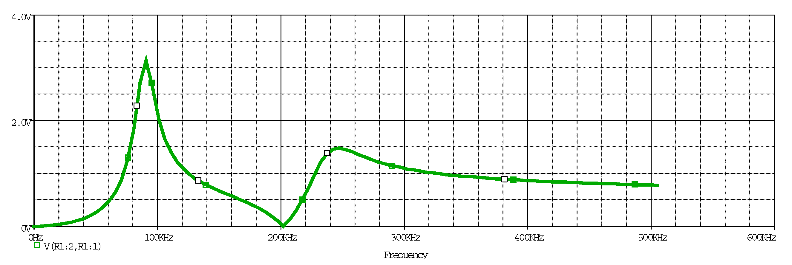
A 400 W pseudo DC link inverter is designed on our proposed topology. The input voltage is 40 V, while the maximum output voltage is 400 V. The load resistance RL is , and . The Q point is 0.25, and the inductance ratio (L) is 3. The switching frequencies for the primary and secondary sides are selected as 200 kz and 50 z, respectively. The switching frequency range is fR1 < fS < fR2, as the gain is evenly divided in this region. We consider CS = CP = and LS = LP =, so that fR1 is 61.8% of fR2 while fR3 is 161.8% of fR2. The and . The magnetizing inductance Lm is . The remaining components used in the inverter are given in Table 1. To verify the components and resonant frequencies of the LLCLC resonant tank, the AC sweep characteristics of the designed resonant tank are determined and shown in Figure 2.

Table 1.
Components and values.

Figure 2.
Alternating Current (AC) sweep characteristics of the designed tank.
4. Simulation Results
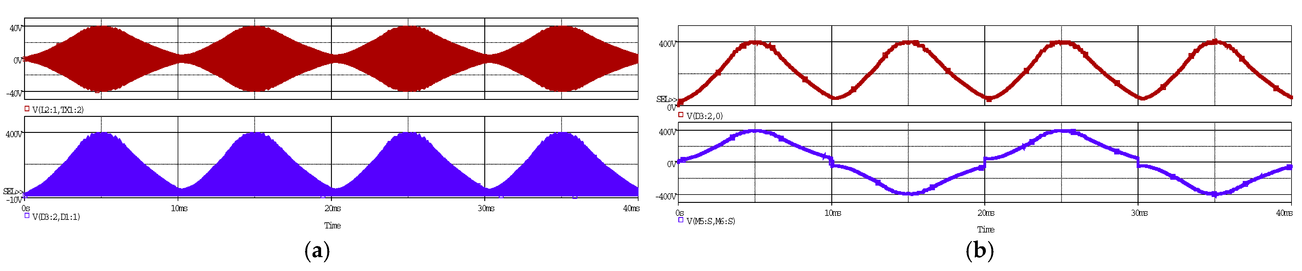
The performance of the purposed inverter is verified and simulated on OrCAD PSpice software. The simulated outputs of the resonant tank and the full-wave rectifier are shown in Figure 3a. The variable input voltage frequency of the resonant tank is between fR1 and fR2. At fR1, the output is approximately equal to the input, so the gain is one. However, at fR2, the tank output is approximately 5 V; therefore, the minimum possible gain is 0.125 which is still much less than conventional LLC resonant tanks. Similarly, the outputs of the DC link and the inverter are also given in Figure 3b. The peak value voltage is approximately 400 V.

Figure 3.
Inverter voltages at different stages: (a) output voltages of the LLCLC tank and the full-wave rectifier; (b) output voltages of the DC link and the inverter output.
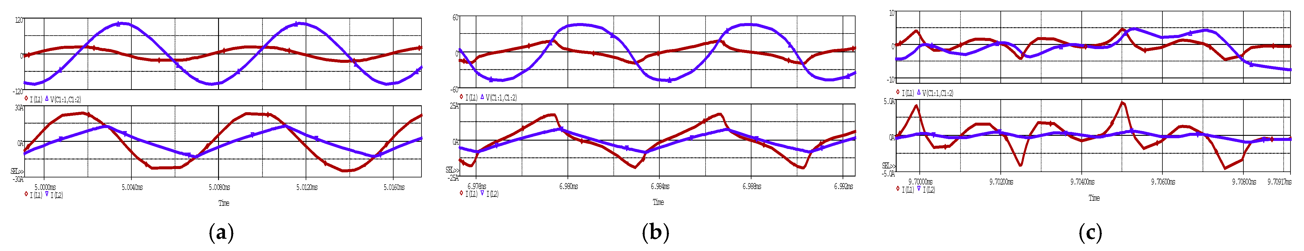
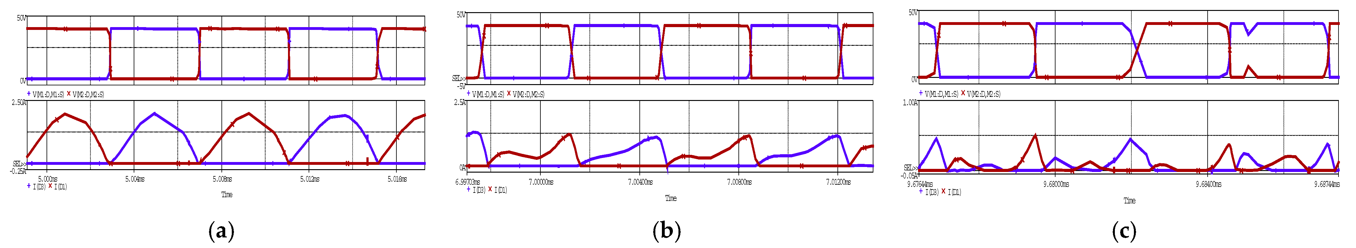
The simulated outputs of drain to the source voltage of MOSFETs w.r.t series resonant inductor current (ILs) of the LLCLC resonant converter at different fs are shown in Figure 4. The voltage is reduced to zero, before the resonant current achieves Zero Voltage Switching (ZVS) through the inverter operation. The third harmonic is added to the resonance current when operating below fR1. The resonant current is approximately zero at the switching frequency of fR2. Figure 5 shows the relation of the series resonant capacitor voltage VCs versus ILs and ILs versus ILm at fR1 ≤ fs ≤ fR2. The current lags the voltage confirming ZVS in these regions. Similarly, the magnetizing current ILm increase and decrease linearly in every cycle. Figure 6 displays the secondary side diodes current according to the primary side voltage at fR1 ≤ fs ≤ fR2. Here, the voltage across diodes is proportional to the switches voltage. The diodes are turned off at a zero current, achieving ZCS across them. At fs = fR2, the current through the diodes is very small.
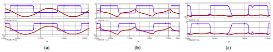
Figure 4.
Current (ILs) w.r.t voltages at S1, S4 and S2, S3: (a) output at fs = fR1; (b) output at fR1 < fs < fR2; (c) output at fs = fR2.
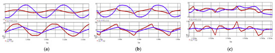
Figure 5.
Current (ILs) w.r.t voltages (VCs) and currents (ILm): (a) output at fs = fR1; (b) output at fR1 < fs < fR2; (c) output at fs = fR2.
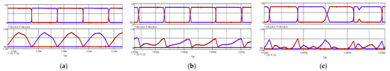
Figure 6.
Rectified current w.r.t voltages at S1, S4 and S2, S3: (a) output at fs = fR1; (b) output at fR1 < fs < fR2; (c) output at fs = fR2.
5. Conclusions
An LLCLC resonant converter-based pseudo DC link inverter topology is proposed. The inverter uses an LLC resonant DC converter topology with an additional LC component providing a 0.125 gain at a resonant frequency fR2 by increasing the impedance of a tank to infinity. The inverter regulates the output voltage by changing the switching the frequency of the primary switches. The inverter provides a rectified DC voltage at the DC link stage, which is unfolded to a sinusoidal voltage by a full-bridge inverter. The performance of a pseudo DC link inverter with the input power of 400 W and the input voltage of 40 V and the output voltage of 400 V was evaluated by simulation on Orcad Pspice.
Conflicts of Interest
The authors declare no conflict of interest.
References
- Abas, N.; Kalair, A.; Khan, N. Review of fossil fuels and future energy technologies. Futures 2015, 69, 31–49. [Google Scholar] [CrossRef]
- Guangul, F.M.; Chala, G.T. Solar energy as renewable energy source: SWOT analysis. In Proceedings of the 2019 4th MEC International Conference on Big Data and Smart City (ICBDSC), Muscat, Oman, 15–16 January 2019. [Google Scholar]
- Narendiran, S. Grid tie inverter and MPPT—A review. In Proceedings of the 2013 International Conference on Circuits, Power and Computing Technologies (ICCPCT), Nagercoil, India, 20–21 March 2013. [Google Scholar]
- Quan, L.; Wolfs, P. A review of the single phase photovoltaic module integrated converter topologies with three different DC link configurations. IEEE Trans. Power Electron. 2008, 23, 1320–1333. [Google Scholar] [CrossRef] [Green Version]
- Pervaiz, S.; Rehman, M.U.; Asghar, A.B.; Zaffar, N. A novel single-phase soft switching microinverter for photovoltaic applications. In Proceedings of the 2013 3rd International Conference on Electric Power and Energy Conversion Systems, Istanbul, Turkey, 2–4 October 2013. [Google Scholar]
- Zhao, Y.; Wei, T.; Hu, H.; Xing, Y. A high-efficiency PV grid-tied micro-inverter with soft switching for dc/ac stage. In Proceedings of the 2015 IEEE 10th Conference on Industrial Electronics and Applications (ICIEA), Auckland, New Zealand, 15–17 June 2015. [Google Scholar]
- Yeh, C.S.; Chen, C.W.; Lee, M.; Lai, J.S. A Hybrid Modulation Method for Single-Stage Soft-Switching Inverter Based on Series Resonant Converter. IEEE Trans. Power Electron. 2019, 35, 5785–5796. [Google Scholar] [CrossRef]
- Lin, R.-L.; Huang, L.-H. Efficiency improvement on LLC resonant converter using integrated LCLC resonant transformer. IEEE Trans. Ind. Appl. 2017, 54, 1756–1764. [Google Scholar] [CrossRef]
- Koscelnik, J.; Frivaldsky, M.; Prazenica, M.; Mazgut, R. A review of multi-elements resonant converters topologies. In Proceedings of the 2014 ELEKTRO, Rajecke Teplice, Slovakia, 19–20 May 2014. [Google Scholar]
- Mazgut, R.; Galad, M.; Kascak, S.; Spanik, P. Analysis of multi-resonant LLCLC converter. In Proceedings of the 2016 ELEKTRO, Strbske Pleso, Slovakia, 16–18 May 2016. [Google Scholar]
- Ren, R.; Zhang, F.; Shen, Z.; Liu, S. The third harmonics current injection scheme for LLC topology to reduce the RMS of the output current. In Proceedings of the 2015 IEEE Applied Power Electronics Conference and Exposition (APEC), Charlotte, NC, USA, 15–19 March 2015. [Google Scholar]

Publisher’s Note: MDPI stays neutral with regard to jurisdictional claims in published maps and institutional affiliations. |
© 2021 by the authors. Licensee MDPI, Basel, Switzerland. This article is an open access article distributed under the terms and conditions of the Creative Commons Attribution (CC BY) license (https://creativecommons.org/licenses/by/4.0/).