Proceeding Paper

Optical Coatings: Applications and Metrology †

1
Institute for Photonics and Nanotechnologies (IFN), National Research Council (CNR), Via Trasea 7, 35131 Padova, Italy
2
Centro di Ateneo di Studi e Attività Spaziali “Giuseppe Colombo”—CISAS, Via Venezia 15, 35131 Padova, Italy
3
Department of Engineering, Università degli Studi della Campania “Luigi Vannvitelli”, Via Roma 29, 81031 Aversa, Italy
*
Author to whom correspondence should be addressed.
Presented at the 2nd International Electronic Conference on Applied Sciences, 15–31 October 2021; Available online: https://asec2021.sciforum.net/.
Eng. Proc. 2021, 11(1), 50; https://doi.org/10.3390/ASEC2021-11137
Published: 15 October 2021
(This article belongs to the Proceedings of The 2nd International Electronic Conference on Applied Sciences)

Abstract

:
The development of optical coatings has experienced rapid growth in the last few decades for a wide range of applications. The strong demand is motivated by the progress of new-generation sources, large-scale facilities, new lithography arrangements, innovative methods for materials science investigation, biosensors, and instruments for space and solar physics observations. The research activities carried out at the Padova branch of the Institute for Photonics and Nanotechnologies of the National Research Council range from the design and characterization of optical components for space activities to the development of nanostructured coatings for tools, such as biosensors and surface plasmon resonance devices. In recent years, we have dealt with the optical characterization of 2D materials in order to explore the feasibility of innovative optical elements designed and optimized to cover wide spectral ranges. In this manuscript, we show the results on the optical characterizations of MoS2 and graphene samples, both monolayers, deposited on thick SiO2 film. We present the preliminary and comparative analysis of the samples in question, showing a direct comparison with the optical performance of the pristine SiO2 over the visible spectral range.

1. Introduction

The Institute for Photonics and Nanotechnologies (IFN) of Italy’s National Research Council (CNR) carries out pioneering research in several fields of photonics. The Padova branch stands out in the technological activities related to the development of optical devices. Applications range from space instrumentation to sensors platforms, including optical metrology, and are strongly oriented to applied physics and technology transfer [1].
Thin films and optical coatings are transversal topics, common to all activities just mentioned. In the field of biosensors development, nanostructured films find a very interesting application in the use of innovative metals for surface plasmon resonance (SPR) platforms based on prism and fiber [2,3]. The scope is to improve sensitivity, detection accuracy, dynamic range, and application fields of this type of biodevice [4,5]. In space optics, high-performance optical coatings are optimized both to fulfill the scientific requirements of the instruments and to survive harsh operation environments [6]. Furthermore, in some spectral regions, such as vacuum ultraviolet and soft X-ray, the structures of the optical films become particularly complex, requiring design and fabrication of multilayer stacks [7].
Over the years, the CNR-IFN focused on the design and characterization of nanostructured thin films to be used as sensitive layers for biosensors [8,9], mirrors [10], filters, phase retarders [11], and polarizers. We have collaborated on the fabrication of a palladium/gold bilayer designed for an SPR sensor based on D-shaped optical fibre (POF). The novel SPR-POF platform was optimized to work in the 1.38–1.42 refractive index range, where it exhibits excellent performances in terms of sensitivity and signal to noise ratio [9].
Another interesting application we dealt with was the development of innovative biochips for Kretschmann SPR tools [8]. The new chips are based on palladium thin films deposited on plastic substrate. The plastic support is low cost and commercially appealing, and the palladium is interesting from the scientific point of view, showing inverted surface plasmon resonance response. The biochips were tested for the detection of DNA chains, selected as the target of the experiment, since they can be applied to several medical early-diagnosis tools, such as different biomarkers of cancers or cystic fibrosis [8].
With regard to characterization and metrology capability, an ellipsometry system dedicated to the study of optical properties, composition, and contamination of materials has been recently developed in the CNR-IFN laboratories [12]. One of the recent applications for this system was the study of the optical performance of a few layers graphene at hydrogen Lyman-alpha (121.6 nm) [13]. We determined the optical constants of such a material at this spectral line and observed the optical anisotropy and the effects induced on the substrate performances as a shift of the pseudo-Brewster angle [13].
Graphene is interesting for several reasons [14]: for example, its excellent chemical and thermal stability [15]. The arrangement of the carbon atoms makes it inert and impermeable to all atomic species, including helium [16]. It is an outstanding candidate as protective layer of optical coatings designed to operate in hostile conditions.
However, graphene is not the only 2D material under investigation. Among the others, MoS2 is appealing for biosensing and optical sensors development [17]. The bio-applications, such as DNA, cancer, and COVID-19 detection, are the most relevant [18], and are supported by a study that shows MoS2 is compatible with human bodies, while graphene is still under study for this aspect. Whatever the potential in optics, any feasibility assessment can be made after a careful evaluation of the optical performance of the materials. We therefore sought to measure the effects of monolayer MoS2 deposited on the top of a widely used substrate. The substrate chosen for this comparative analysis was a thick SiO2 film. The SiO2 is well known due to excellent properties, such as anti-resistance, hardness, corrosion resistance, dielectric, and optical transparency [19,20,21].
Starting from this scenario, we characterized the optical response of MoS2 in the visible spectral range under light polarization control and compared its optical throughput with that of graphene, the most popular of the 2D materials, and pristine SiO2.
We describe the preliminary results in this manuscript, that includes a section dedicated to the experimental equipment and samples, and a section dedicated to the experimental achievements and discussion. The conclusion reports a summary of what is presented in the paper by envisioning a future experimental campaign.

2. Experimental Arrangement and Samples

The samples whose measurements we report in this paper are:
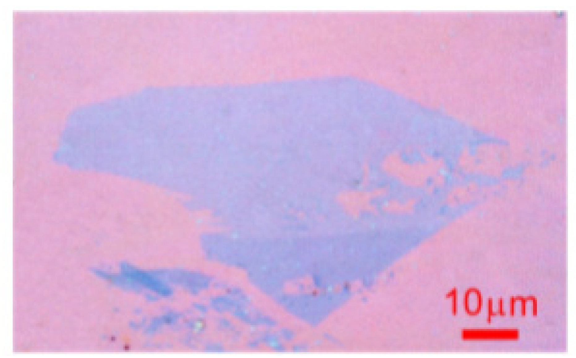
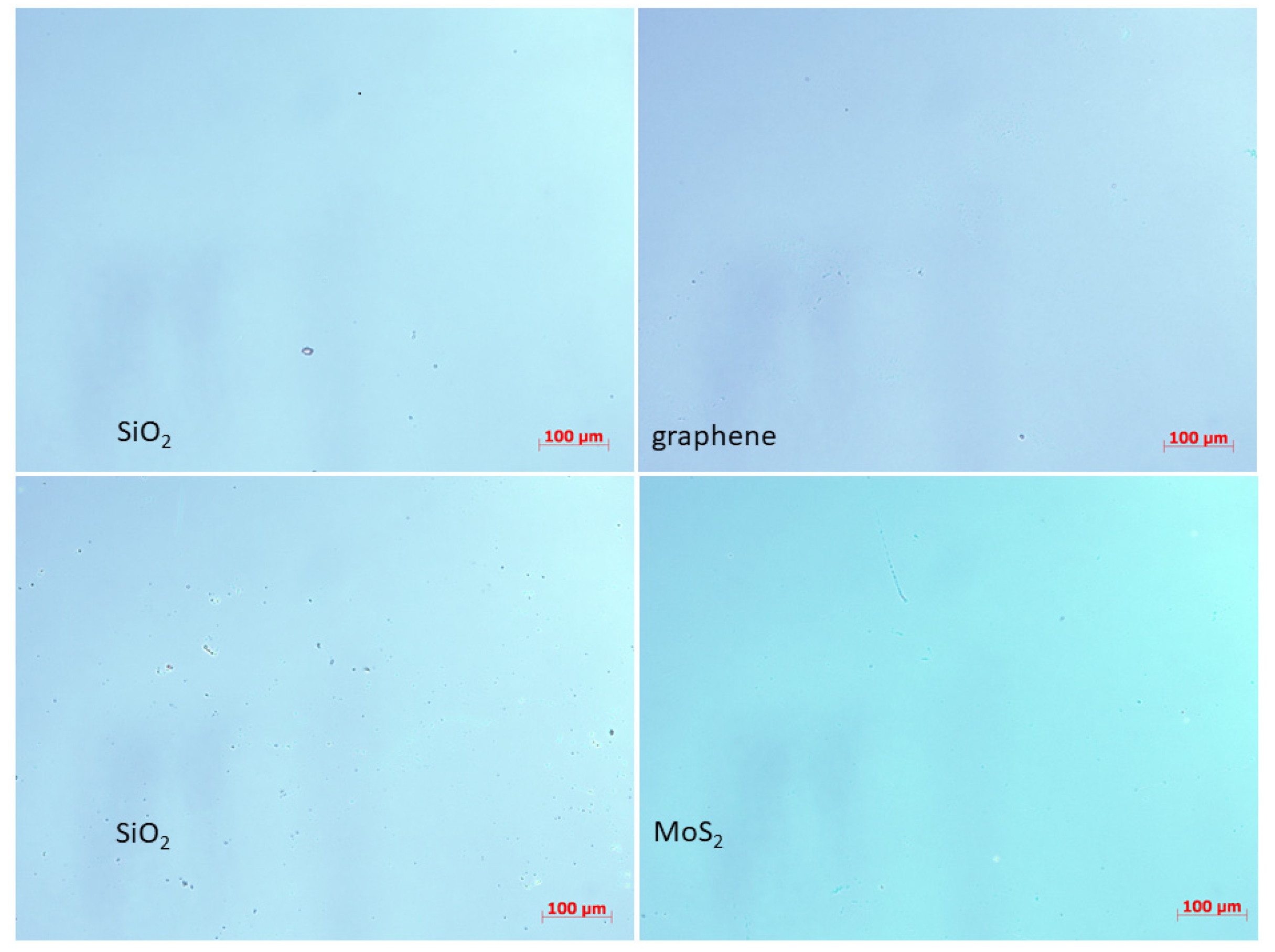
  • Monolayer graphene onto SiO2 (300 nm)/Si and the corresponding bare sample of SiO2 (300 nm)/Si (named “SiO2 [R-G), both provided by Graphenea, Inc.;
  • Monolayer of MoS2 onto SiO2 (300 nm)/Si and the corresponding bare sample of SiO2 (300 nm)/Si, (named “MoS2 [R-MoS2]”), both provided by 2D semiconductors.
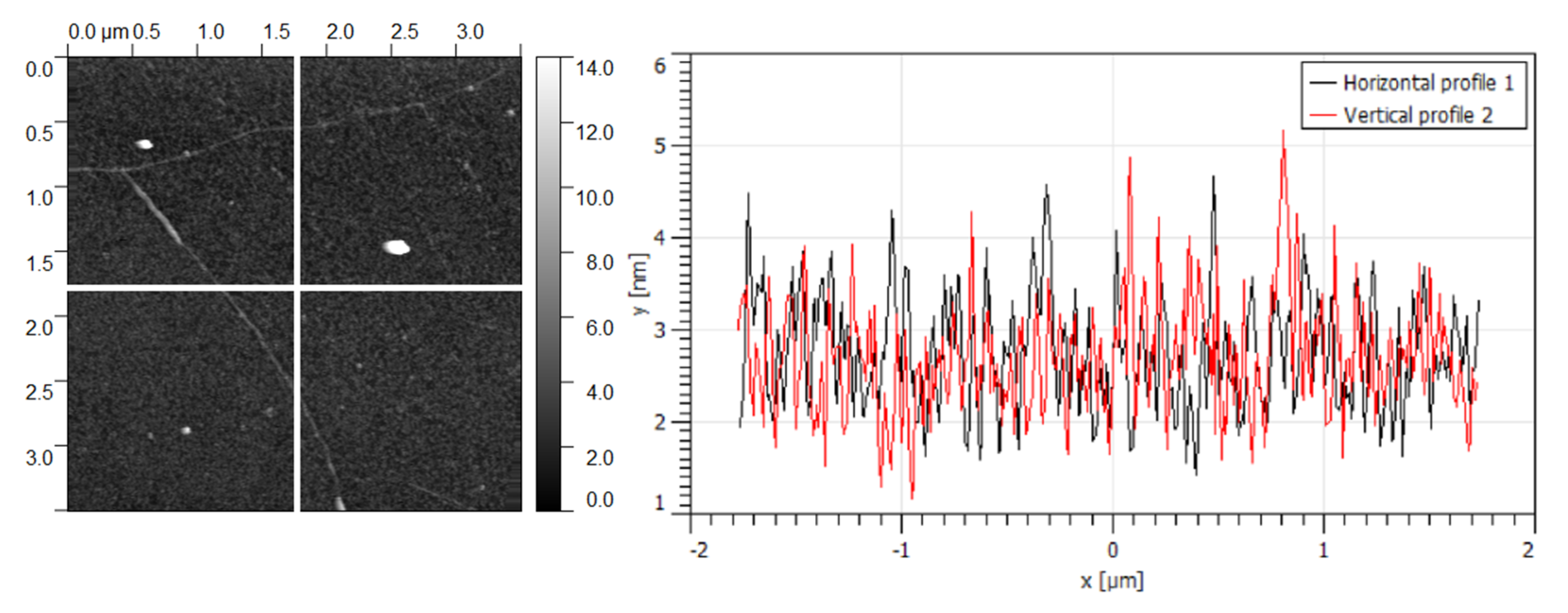
The thicknesses of the graphene and MoS2 were not experimentally determined at the time of this manuscript, but this is planned as part of the measurement campaign we have planned. We want to use Raman spectroscopy for this purpose, as we have already for the study of the three-layer graphene in [13]. Then, we are referring to “monolayer”, according to what it is declared by the suppliers.
The nominal thickness of SiO2 is 300 nm. The reflectivity measurements described hereafter make it possible to estimate the value from the experimental measurement test.
A proper thickness of the SiO2 substrate allows the direct observation of graphene and MoS2 by optical microscope. In mono layered graphene and MoS2 materials, few layers, discontinuities, and wrinkles are directly detectable in a very simple way [22,23,24,25]. The first measurement performed on the samples under examination was an observation by optical microscope. The images were acquired at 100× magnification.
We also investigated the morphology of the monolayer graphene sample by atomic force microscope (AFM) in no-contact mode operation (Park System XE-70).
After the observation of the surface, the samples were characterized in terms of optical performance.
The reflectometers equipment available at the CNR-IFN laboratories located in Padova cover a wide spectral range extending from the extreme ultraviolet (EUV) to visible wavelengths. An additional tool for infrared measurements has also recently been acquired.
The optical characterizations at shorter wavelengths (30–400 nm) require the use of normal incidence Johnson–Onaka reflectometer operating in vacuum. Figure 1 exhibits the sketch of the device [13].
The dispersion element mounted on the reflectometer is a Pt-coated toroidal grating with 600 lines/mm. The main radius is 0.5 m and the subtended angle between the entrance and the exit slits is 25°. A toroidal mirror working at 45° incidence angle focuses the monochromatic radiation on the sample. In the experimental chamber, the samples are hosted on a holder that can be rotated to the desired incidence angle. We have recently implemented this facility with a rotating linear polarizer optimized for the VUV. In this way, the reflectometer is suitable for ellipsometry measurements [12,13]. The upgraded system has recently been used for the characterization of phase retarders for EUV-VUV wavelengths [12,13].
The optical characterization in the visible spectral range is accomplished by using the VIS reflectometer depicted in Figure 2. The system designed for testing the optical response of samples at variable incidence angles, working in a θ-2θ configuration, was recently assembled. It consists of a compact, stabilized, broadband light source (360–2600 nm), a rotator stage to hold the sample at a desired working angle, and a spectrometer coupled with a cosine corrector for the detection.
The measurements, in reflection and transmission modes, can be performed for any type of sample with no restrictions in size. The optical response can be tested with polarized and unpolarized light in order to investigate the polarization response of the specimen of interest. A commercial polarizing filter was used in the measures described in this paper [25]. The filter has a p-polarized transmission close to 90% in the spectral range 450–900 nm. A calibrated sample of protected aluminium was used as a reference specimen (Filmetrics KLA Corporation).

3. Results

In the sample under analysis, the nominal thickness (300 nm) of the pristine SiO2 is tuned to enhance the optical visibility of the 2D materials on the top [22,23,24,25]. The top surface quality of graphene and MoS2 can be easily determined by using an optical microscope, that allowed us to estimate the linear dimensions of the superficial defects. The presence of film discontinuities and wrinkles can be assessed in a qualitative and semi-quantitative way over a wide region. In case of regions of the same sample with a different number of layers, we usually observe areas with different contrast. An illustrative example is depicted in Figure 3 [24]. The image by Y. Stubrov et al. [24] shows a graphene plate on a Si substrate, covered with 300 nm-thick SiO2 layer.
For the specimens characterized in this paper, we cannot determine how many layers there are, but we can say that the number of layers is the same in all regions of the sample. The images (see Figure 4), acquired by a camera connected to the optical microscope, show a good quality of the samples surface, good homogeneity for both monolayers, and no relevant defects.
Several areas of the specimens were observed; we report the representative ones.
Figure 5 depicts the surface of the graphene sample (left) analysed by AFM over 3.5 µm × 3.5 µm area. At the time of writing, we have only analysed the AFM measurements of graphene, but we plan to perform the characterization on all samples under study. The surface quality of the graphene is good even at the nm scale, showing some wrinkles and defects mainly due to the transfer process of graphene, grown by chemical vapor deposition and then transferred onto SiO2 substrate. The roughness estimated on the profiles (right) corresponding to the white cross in Figure 4 is Ra = 0.6 nm and Rq = 0.75 nm.
Once the samples were observed by optical microscope, their optical performance was measured. The experimental results are reported in Figure 6. All tests have been performed at 8° angle of incidence by using p-polarized light as probe.
In this test campaign, we used a known reference sample dealt by Filmetrics KLA Corporation for determining the experimental reflectance of any sample, without measuring the direct beam and without moving the experimental arrangement.
It is required to determine the factor F (Equation (1)):
F = R r e f R c a l
which is the ratio between the value of the light reflected by the reference sample (Rref) and the reflectance of the same sample measured and certified by the manufacturer (Rref).
Given the experimental value of the light reflected by the specimen that we want to characterize (Rexp), the experimental reflectance, R, of such as sample is given by the following relationship:
R = R e x p F
Figure 6 shows the measured reflectance according to Equation (2) for the four samples we are analysing. It is worth to note that the performances of the two SiO2 provided by Graphenea, Inc. (see Figure 5, “SiO2 [R-G] exp”) and 2D semiconductors (see Figure 5, “SiO2 [R-MoS2] exp”), even if they come from two different suppliers, are both in good agreement with the simulation of the structure SiO2 (315 nm)/Si. Then, the actual thickness of the SiO2 that we can estimate from the reflectance measurements is 315 nm.
The reflectance of the SiO2 is the reference with respect to we want to observe the optical effects of 2D materials. The sample with graphene on the top (see Figure 5, “graphene exp”) reflects sensitively less and shows a blue shift of the minimum, that occurs around 605 nm against 610 nm of SiO2. On the contrary, MoS2 (see Figure 5, “MoS2 exp”) induces a red shift of the minimum, which is observed around 640 nm. The reflectance is higher than that of SiO2 up to 580 nm, then becomes significantly lower at longer wavelengths.
The present study is qualitative and shows how reflectance measurements with polarization control are sensitive to the presence of 2D materials on the surface of a SiO2/Si substrate, despite the sub-nanometric structures (nominal thickness of monolayer graphene is 0.34 nm and nominal thickness of monolayer MoS2 is 0.72 nm). For a quantitative analysis, we plan to perform experimental thickness measurements and a full characterization on samples with different thicknesses of graphene and MoS2.
Combined with experimental determination of thicknesses, the reflectance response can be used to retrieve the optical constants of such a material at the wavelength of interest. For graphene, this analysis has been addressed by several authors; for MoS2, there are still interesting studies that could be assessed.

4. Conclusions

In this manuscript, we analysed the optical response of four samples based on the structure SiO2/Si, two of them capped by MoS2 and graphene, respectively. The experimental results show a good sensitivity of the reflectance to 2D materials, offering great potential for their characterization in view of many application scenarios.

Author Contributions

Conceptualization P.Z., methodology P.Z. and P.C., validation P.Z. and P.C., formal analysis P.Z., investigation, resource, data curation P.Z., P.C., C.C., S.N., N.C., L.Z., V.D.D., writing-original draft preparation P.Z., writing-review and editing P.Z., P.C., C.C., S.N., N.C., L.Z., V.D.D., visualization, supervision P.Z., project administration P.Z., funding acquisition V.D.D. All authors have read and agreed to the published version of the manuscript.

Funding

This activity has been financially supported by the contracts n. 2020-4-HH.0 and n. 2019-34-HH.0 between Agenzia Spaziale Italiana (ASI) and the Istituto Nazionale di Astrofisica (INAF).

Institutional Review Board Statement

Not applicable.

Informed Consent Statement

Not applicable.

Data Availability Statement

Not applicable.

Conflicts of Interest

The authors declare no conflict of interest.

References

  1. Available online: http://www.pd.ifn.cnr.it (accessed on 1 April 2022).
  2. Yesudasu, V.; Shekhar Pradhan, H.; Jasvanthbhai Pandyab, R. Recent progress in surface plasmon resonance based sensors: A comprehensive review. Heliyon 2021, 7, e06321. [Google Scholar] [CrossRef] [PubMed]
  3. Zeng, Y.; Zhou, J.; Sang, W.; Kong, W.; Qu, J.; Ho, H.P.; Zhou, K.; Zhi Gao, B.; Chen, J.; Shao, Y. High-Sensitive Surface Plasmon Resonance Imaging Biosensor Based on Dual-Wavelength Differential Method. Front. Chem. 2021, 9, 801355. [Google Scholar] [CrossRef] [PubMed]
  4. Cai, H.; Shan, S.; Wang, X. High Sensitivity Surface Plasmon Resonance Sensor Based on Periodic Multilayer Thin Films. Nanomaterials 2021, 11, 3399. [Google Scholar] [CrossRef]
  5. Zhu, J.; Li, N. Novel high sensitivity SPR sensor based on surface plasmon resonance technology and IMI waveguide structure. Results Phys. 2020, 17, 103049. [Google Scholar] [CrossRef]
  6. Garoli, D.; Rodriguez De Marcos, L.V.; Larruquert, J.I.; Corso, A.J.; Proietti Zaccaria, R.; Pelizzo, M.G. Mirrors for Space Telescopes: Degradation Issues. Appl. Sci. 2020, 10, 7538. [Google Scholar] [CrossRef]
  7. Slaughter, J.M.; Schulze, D.W. Structure and performance of Si/Mo multilayer mirrors for the extreme ultraviolet. J. Appl. Phys. 1994, 76, 2144. [Google Scholar] [CrossRef]
  8. Zuppella, P.; Pasqualotto, E.; Zuccon, S.; Gerlin, F.; Corso, A.J.; Scaramuzza, M.; De Toni, A.; Paccagnella, A.; Pelizzo, M.G. Palladium on Plastic Substrates for Plasmonic Devices. Sensors 2015, 15, 1138–1147. [Google Scholar] [CrossRef] [Green Version]
  9. Cennamo, N.; Zuppella, P.; Bacco, D.; Corso, A.J.; Pelizzo, M.G.; Zeni, L. SPR Sensor Platform Based on a Novel Metal Bilayer Applied on D–Shaped Plastic Optical Fibers for Refractive Index Measurements in the Range 1.38–1.42. IEEE Sens. J. 2016, 16, 4822–4827. [Google Scholar] [CrossRef]
  10. Zuppella, P.; Monaco, G.; Corso, A.J.; Nicolosi, P.; Windt, D.L.; Bello, V.; Mattei, G.; Pelizzo, M.G. Iridium/silicon multilayers for extreme ultraviolet applications in the 20–35 nm wavelength range. Opt. Lett. 2011, 36, 1203–1205. [Google Scholar] [CrossRef]
  11. Gaballah, A.E.H.; Nicolosi, P.; Ahmed, N.; Jimenez, K.; Pettinari, G.; Gerardino, A.; Zuppella, P. Vacuum ultraviolet quarter wave plates based on SnTe/Al bilayer: Design, fabrication, optical and ellipsometric characterization. App. Surf. Sci. 2019, 463, 75–81. [Google Scholar] [CrossRef]
  12. Gaballah, A.E.H.; Nicolosi, P.; Ahmed, N.; Jimenez, K.; Pettinari, G.; Gerardino, A.; Zuppella, P. EUV polarimetry for thin film and surface characterization and EUV phase retarder reflector development. Rev. Sci. Instrum. 2018, 89, 015108. [Google Scholar] [CrossRef] [PubMed] [Green Version]
  13. Malik, N.A.; Nicolosi, P.; Jimenez, K.; Gaballah, A.; Giglia, A.; Lazzarino, M.; Zuppella, P. Experimental Study of Few-Layer Graphene: Optical Anisotropy and Pseudo-Brewster Angle Shift in Vacuum Ultraviolet Spectral Range. Adv. Photonics Res. 2021, 2, 2000207. [Google Scholar] [CrossRef]
  14. Geim, A.K.; Novoselov, K.S. The rise of graphene. Nat. Mater. 2007, 6, 183–191. [Google Scholar] [CrossRef] [PubMed]
  15. Galashev, A.; Rakhmanova, O. Mechanical and thermal stability of graphene and graphene-based materials. Phys. Uspekhi 2014, 57, 970–989. [Google Scholar] [CrossRef]
  16. Su, Y.; Kravets, V.G.; Wong, S.L.; Waters, J.; Geim, A.K.; Nair, R.R. Impermeable barrier films and protective coatings based on reduced graphene oxide. Nat. Commun. 2014, 5, 5843. [Google Scholar] [CrossRef]
  17. Zhang, W.; Zhang, P.; Su, Z.; Wei, G. Synthesis and sensor applications of MoS2-based nanocomposites. Nanoscale 2015, 7, 18364–18378. [Google Scholar] [CrossRef]
  18. Zhao, L.; Kong, D.; Wu, Z.; Liu, G.; Yan, X.; Liu, F.; Liu, X.; Wang, C.; Cui, J.; Lu, G. Interface interaction of MoS2 nanosheets with DNA based aptameric biosensor for carbohydrate antigen 15–3 detection. Microchem. J. 2020, 15, 104675. [Google Scholar] [CrossRef]
  19. Gitlin, D.; Karp, J.; Moyzhes, B. Graded tunnelling barrier and oxygen concentration in thermally grown ultrathin SiOx gate oxide. J. Phys. D Appl. Phys. 2007, 40, 2143–2149. [Google Scholar] [CrossRef]
  20. Gravalidis, C.; Gioti, M.; Laskarakis, A.; Logothetidis, S. Real-time monitoring of silicon oxide deposition processes. Surf. Coat. Technol. 2004, 180−181, 655–658. [Google Scholar] [CrossRef]
  21. Aharonovich, I.; Lifshitz, Y.; Tamir, S. Growth mechanisms of amorphous SiO[sub x] nanowires. Appl. Phys. Lett. 2007, 90, 263109. [Google Scholar] [CrossRef]
  22. Blake, P.; Hill, E.W. Making graphene visible. Appl. Phys. Lett. 2007, 91, 063124. [Google Scholar] [CrossRef] [Green Version]
  23. Zhang, X.; Kawai, H.; Yang, J.; Goh, K.E.J. Detecting MoS2 and MoSe2 with optical contrast simulation. Prog. Nat.Sci. Mater. Int. 2019, 29, 667–671. [Google Scholar] [CrossRef]
  24. Stubrov, Y.; Nikolenko, A.; Strelchuk, V.; Nedilko, S.; Chornii, V. Structural Modification of Single-Layer Graphene Under Laser Irradiation Featured. Nanoscale Res. Lett. 2017, 12, 297. [Google Scholar] [CrossRef] [PubMed] [Green Version]
  25. Xu, H.; Zhou, W.; Zheng, X.; Huang, J.; Feng, X.; Ye, L.; Xu, G.; Lin, F. Control of the Nucleation Density of Molybdenum Disulfide in Large-Scale Synthesis Using Chemical Vapor Deposition. Materials 2018, 11, 870. [Google Scholar] [CrossRef] [Green Version]
Figure 1. The figure used under CC-BY 4.0 depicts the EUV-VUV-UV Johnson–Onaka reflectometer.
Engproc 11 00050 g001
Figure 2. The design and the photograph exhibit the reflectometer available at CNR-IFN in Padova and optimized for the optical characterization in the visible range.
Engproc 11 00050 g002
Figure 3. The figure used under CC-BY 4.0 depicts the optical microscopy image of an investigated graphene sample located on Si substrate, covered with 300 nm-thick SiO2 layer.
Engproc 11 00050 g003
Figure 4. The figure depicts regions of the samples: SiO2 provided by Graphenea (left, top); graphene provided by Graphenea (right, top); SiO2 provided by 2D semiconductors (left, bottom); MoS2 provided by 2D semiconductors (right, bottom).
Engproc 11 00050 g004
Figure 5. The figure depicts AFM measurement (left) of the graphene sample provided by Graphenea (left, top); the horizontal and vertical profiles (right) correspond to the white cross.
Engproc 11 00050 g005
Figure 6. The plot depicts the experimental p-reflectance of the four samples under investigation together with the simulation of a SiO2 (315 nm)/Si.
Engproc 11 00050 g006
Publisher’s Note: MDPI stays neutral with regard to jurisdictional claims in published maps and institutional affiliations.

