Abstract
We developed an artificial intelligence (AI) model to optimize the time efficiency, yield, and energy efficiency of the semiconductor coating process. A random forest-based model was developed for rapid modeling and analysis of the semiconductor coating process, thus allowing designers and operation managers to conduct an efficient and effective process. The developed AI model offers an objective and accurate basis for decision-making, thereby ensuring that each unit is operated energy-efficiently, stably, and reliably in the minimized operation time. The developed model assists Taiwan’s semiconductor industry in transitioning from engineer experience to data-driven approaches, thus accelerating the technological optimization of semiconductor factories and adding value to customers. This model considerably reduces the material, energy, resource, time, labor, and costs of thin film deposition. The model allows the semiconductor industry of Taiwan to consolidate its competitive advantage by achieving net-zero carbon emissions and sustainability.
1. Semiconductor Coating Process
The semiconductor industry is technology-intensive and evolving rapidly. In line with Moore’s law, the component feature sizes continue to shrink, and the number of transistors on a single integrated circuit chip doubles every 12 months. The current development trend in semiconductor manufacturing technology is moving toward larger wafer sizes and smaller line widths. Most semiconductor devices are developed according to the varying numbers of stacked thin films with different thicknesses.
The technology to deposit these films on the wafer surface is called thin film deposition [1]. In general, thin film deposition technologies are classified into physical vapor deposition (PVD) and chemical vapor deposition (CVD) technologies. In PVD, physical methods, such as heating or sputtering, are used to vaporize solid materials. The vapors are then recondensed onto the wafer surface to produce solid thin films. In contrast, CVD involves the use of chemical methods in which gaseous source materials undergo chemical reactions on the wafer surface, resulting in the deposition of solid thin films. Although both methods have advantages and limitations, PVD is more appropriate for the deposition of metallic thin films, whereas CVD is widely applied to various types of thin film deposition, including epitaxial silicon deposition, polysilicon deposition, dielectric film deposition, and metallic thin film deposition. Furthermore, the step coverage of thin films deposited through CVD is considerably larger than that of thin films deposited using PVD. Therefore, CVD has been extensively developed and applied.
CVD is a process technology in which gaseous reactants are used to produce solid products in thin films on a wafer. In a CVD system, highly reactive gaseous precursor materials are used as source materials to produce the target coating layers. These precursors are combined with reactive gases, such as oxygen, nitrogen, hydrogen, and ammonia. The gas mixtures are simultaneously introduced into the process chamber, in which they undergo chemical reactions to produce thin films. CVD is most commonly used to prepare oxide and nitride films. For example, silane (SiH4) is combined with oxygen and ammonia to produce silicon dioxide (SiO2) and silicon nitride (Si3N4) films, respectively. The film growth process typically involves chemical oxidation, chemical reduction, thermal growth, and thermal decomposition. Various CVD processes are incorporated into different vacuum, plasma, high-temperature, and microwave systems for specialized applications.
In the plasma-enhanced CVD (PECVD) system, precursors and reactive gases are sprayed into the vacuum chamber from the top of the chamber. A radio frequency power source is placed between the showerhead and the chamber wall, making the precursors and reactive gases dissociate and form a plasma. The thin film materials then acquire energy and undergo uniform chemical reactions, resulting in an optimal elemental ratio. Subsequently, the reacted materials settle onto the substrate because of gravity. On the substrate surface, these materials are influenced by substrate heating, which induces their lateral movement. Finally, the materials remain at the position of minimum energy on the substrate surface, gradually forming point structures, island structures, mesh structures, and ultimately, continuous thin films.
The key process parameters that affect thin film quality in PECVD are chamber pressure, radio frequency power, flow rates of the precursors and reactive gases, gas flow rate during vacuum pumping, substrate temperature, substrate bias voltage, ambient temperature, and temperature and flow rate of cooling water. Chamber pressure affects the flow rate of the precursors and the reactive gases, and the pumping speed. The lower the chamber pressure during PECVD, the higher the material purity and thin film quality, but the lower the deposition rate. Radio frequency power influences the dissociation capability of the precursor and reactive gases. The higher the power, the higher the dissociation and reaction rates. An optimal radio frequency power level exists for each material. Excessive or insufficient radio frequency power leads to poor thin film quality. Furthermore, an increase in power leads to ion bombardment on the substrate, which damages the bonds of deposited materials. The flow rates of the precursors and reactive gases determine the optimal elemental ratio for the compound formation of materials that are less likely to synthesize with each other.
However, excessive flow rates result in considerable material waste and overly porous thin film structures. Excessive and insufficient flow rates lead to poor thin film quality. For example, the optimal Si:O atomic ratio for SiO2 is 1:2. Achieving this ratio in practice is difficult; therefore, excessive oxygen is typically introduced during PECVD. The gas flow rate during vacuum pumping influences the degree to which the main valve opens. Higher gas flow rates reduce the residence time of compounds on the substrate surface, thereby decreasing the deposition rate and the effect of the gas flow rate on thin film quality varies. For materials such as HfO2, slower growth is required to achieve higher thin film quality, whereas for Cu, faster growth is required to achieve higher thin film quality.
The substrate temperature is one of the most crucial parameters in PECVD, and it affects thin film uniformity, the process temperature required for compound formation, and substrate compatibility. The ideal substrate temperature depends on the process material and the temperature uniformity of the chamber. An optimal substrate temperature exists for each material, and poor thin film quality is obtained when the temperature is too high or low. Substrate bias voltage affects the chemical bonding of the deposited thin film. The application of an external bias voltage results in gas ions bombarding the substrate, enabling the deposited thin film to incorporate the desired elements and achieve the optimal atomic ratio. At this ratio, the electrical and optical properties of the thin film reach their optimal performance. A higher bias voltage increases ion bombardment, improving thin film quality. However, if the voltage exceeds a threshold, it deteriorates existing bonds, causing an etching effect and reducing thin film quality. An optimal substrate bias voltage exists for each material. If the voltage is too high or low, the thin film quality tends to deteriorate.
Ambient temperature has a considerable effect on certain vacuum pumps, causing a marked decline in their vacuum pumping efficiency. For example, turbo pumps and dry pumps may experience decreased performance under only a 2–3 °C change in indoor temperature (this performance can be assessed using a vacuum gauge). This phenomenon changes the chamber base pressure, which results in shifts in process parameters and affects thin film quality. Overall, an increase in ambient temperature leads to a noticeable decline in thin film quality.
Cooling water is mainly used to cool the PECVD equipment during standby and processing, preventing equipment failure caused by excessive heat or O-ring aging and cracking, which damages the vacuum seal. In general, lower cooling water temperatures are preferred, as they prevent heat accumulation in the radio frequency power source, facilitating maximum power output. A lower base pressure in the process chamber also improves thin film quality. A higher flow rate of the cooling water increases the amount of heat removed per unit of time, effectively reducing the overall system temperature. Therefore, lower cooling water temperatures and higher cooling water flow rates lead to a marked improvement in thin film quality.
The main processes responsible for the energy consumption in a CVD system are the heating of the substrate platform and combustion chamber, the use of the radio frequency power source, and the operation of the vacuum pumps. A portion of the adopted materials adheres to the chamber walls or is extracted from the chamber by the vacuum pumps to the combustion chamber for treatment before reaching the substrate and undergoing chemical reactions. Therefore, material wastage becomes particularly severe in CVD systems. In particular, CVD systems make extensive use of organometallic precursors, which are highly toxic, explosive, and polluting. Consequently, CVD systems must be used with combustion chambers or adsorption towers. If the aforementioned materials are not appropriately treated, they pose serious hazards to human health and the environment. Therefore, increasing the utilization efficiency of precursor materials and maintaining pollutant monitoring records are particularly crucial when the CVD system is used.
2. Intelligent Coating Process
The semiconductor coating process is highly specialized as it generally relies on engineers with extensive coating experience to set, adjust, and optimize process parameters. It is necessary to inspect thin film quality and regulate environmental conditions, such as temperature and humidity. The number of variable factors that must be monitored and controlled often increases exponentially with the scale of the process and the required level of thin film quality. This phenomenon increases the workload of engineers and presents challenges in managing numerous variables. Such difficulties result in trade-offs between different variables, ultimately resulting in substantial time, labor resources, and financial resources being expended without achieving the desired outcomes. Furthermore, differences in engineers’ professional proficiency and experience introduce uncertainty and bias in parameter control, increasing the likelihood of inefficient or unsuccessful process outcomes.
Currently, intelligent coating technologies are still in development. The “Smart Process System for Advanced Semiconductor Thin Film Equipment” developed by the Industrial Technology Research Institute (ITRI) [2] in Taiwan is representative of current intelligent coating technologies. This system integrates theoretical models and measurement data to establish a multi-physics analytical model for simulating the thin film quality under different parameter settings. Engineers only need to input different parameter combinations to predict the thin film quality in advance, which considerably shortens the time required for equipment adjustment as well as trial and error. When manual adjustments are employed in the semiconductor coating process, the equipment adjustment time, the development time for new products, the repeatability error for each process cycle, and the prediction accuracy for film quality are 1 week, 3 months, >4%, and <80%, respectively. The system of the ITRI enables the aforementioned parameters to be improved to 2 h, 1 month, <2%, and >95%. Compared with manual adjustments, this system considerably reduces the equipment adjustment time, shortens the development time for new products, decreases the repeatability error for each process cycle, and increases the prediction accuracy for film quality.
The development of intelligent manufacturing is inevitable. A cyber-physical system (CPS) [3] is the core system for realizing intelligent manufacturing. The capabilities of fully intelligent manufacturing methods considerably exceed those of current automated production methods, featuring a high degree of autonomy and self-sufficiency and enabling fully unmanned operations. In intelligent manufacturing, all raw materials, components, workpieces, and finished products move along the production line according to predetermined pathways. Machines on the production line communicate with each other through machine-to-machine (M2M) messages and process workpieces according to preset production parameters and conditions while maintaining effective self-control and autonomous operation. The goal of all operations is grounded in optimization. To achieve the ideal state of intelligent manufacturing, a CPS must be used with various M2M tools, such as sensors, augmented-reality technology, and virtual-reality technology.
A CPS is an integrated system that combines physical and virtual computational models. With sensors, data acquisition systems, and computer networks, a CPS realizes self-perception, decision-making, and control, thereby achieving comprehensive intelligence. It manifests in four key directions: The Internet of Things (IoT), full integration, real-time precision big data, and comprehensive innovation and transformation within enterprises. The applications of this technology extend beyond manufacturing; the technology is also used in other industries. In the transition from Industry 3.0 to 4.0, CPSs have become the core technology for upgrading automated manufacturing to fully intelligent manufacturing. Therefore, these systems substantially transform advanced manufacturing industries. An effective and well-functioning CPS fundamentally depends on accurate, reliable, robust, stable, and rapidly responsive AI models and their algorithms.
3. AI Prediction Models for PVD Coating Process
For modeling, a dataset consisting of n records, denoted as {(X1, Y1), …, (Xn, Yn)}, was considered, where X represents the independent variables in the dataset, and Y represents the dependent variables. The adopted machine-learning models are described as follows.
3.1. Polynomial Regression Model
Regression analysis is used to examine the quantitative relationship between a criterion variable y (also called the dependent variable or explained variable) and a predictor variable x (also called the independent variable or explanatory variable), with an equation being formulated to describe this relationship. This equation is used to predict the criterion variable.
In engineering and science, data obtained through observation or experiments are often described using a specific relational equation. The collected data are represented as a set of paired values (xi, yi), where i = 1, 2, 3, …, n, and are plotted on a coordinate plane. A smooth curve is then drawn through these points, referred to as an approximation curve, and the equation of this curve is used to represent the approximate relationship between x and y. Using an empirical equation and curve fitting, inherent errors are identified and each data point is matched to a regression line precisely. Regression analysis is used to minimize the sum of squared differences between the data points and the curve to derive the desired curve equation (function). The least squares method is used to determine a linear regression equation. However, most engineering and scientific data do not exhibit linear characteristics. If a linear regression model is used to fit such data, considerable errors may occur. In this case, polynomial regression analysis is preferable for fitting the data.
A polynomial regression model includes multiple independent variables in different powers. In applications, the corresponding curve models become extensive because polynomial regression is a special case of general linear regression. When a data series exhibits long-term variation and the rate of variation changes over time, polynomial regression analysis is used to describe the trends or relationships. Its general form is as follows.
y = a0 + a1x + a2x2 + a3x3 + a4x4 + … + anxn + e
To obtain the least squares fit and solve for the regression coefficients, partial differentiation must be used as follows.
If the partial derivatives are equal to 0, the following equations become valid.
The aforementioned nonlinear equations are expressed in matrix form as follows.
After this matrix is simplified, XA = Y, and A = X−1Y are obtained.
3.2. Backpropagation Neural Network
An artificial neural network (ANN) is a data processing model that mimics the structure of the human brain’s neural system. Specifically, ANN uses numerous artificial neurons to simulate the capabilities of biological neural networks. An artificial neuron is a simulation of a biological neuron. It obtains information from the external environment or other artificial neurons, performs simple computations, and outputs computational results to the external environment or other artificial neurons. ANN has the abilities of learning, reasoning, memory, recognition, and adaptation to unknown environmental changes.
ANN comprises many layers of artificial neurons. The operation of an artificial neuron is illustrated in Figure 1. The relationship between its output value Yk and its input value is expressed as
where netk represents the difference between the weighted sum of the input values and the bias value, denotes the weight of a neuron connection, is the bias value, and f represents a nonlinear activation function.
Yk = f (netk)
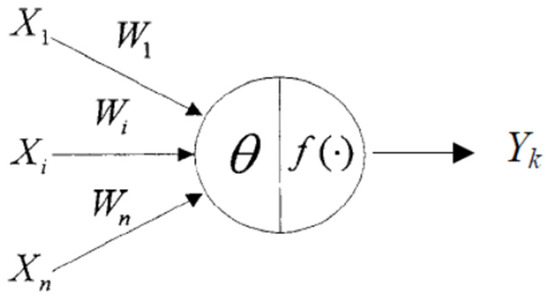
Figure 1.
Operation of artificial neuron.
When ANN is applied to a continuous system, a sigmoid function is often used as the network’s nonlinear activation function (Figure 2). During the learning process of the neural network, the bias values of neurons and the weights of neuron connections are continuously adjusted. Eventually, the bias values and weights gradually stabilize, indicating that the learning process is completed.
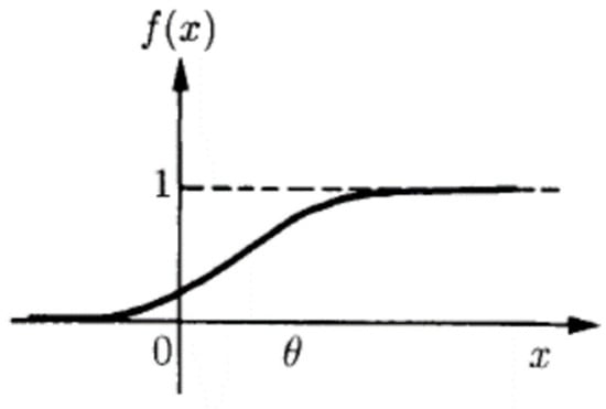
Figure 2.
Sigmoid function.
Backpropagation neural networks (BPNNs) [4,5] are the most commonly applied ANN. The first BPNN model was developed by Rumelhart and McClelland in 1985 for parallel distributed information processing. BPNN models are mainly used for prediction, classification, diagnosis, and other applications. BPNN applies the chain rule of calculus to solve the loss function. A schematic of BPNN is shown in Figure 3. This network mainly consists of three layers. The first layer is the data input layer. The circles and red lines in Figure 3 represent neurons and neuron connection weights, respectively. The second layer is the hidden layer, which mainly performs neuron transformation. This process is expressed as follows: , where represents the neurons in the hidden layer, denotes the neuron connection weights, represents the biases, and denotes the activation function. The activation function allows the model to perform structural transformations, such as those involving the conversion of linear functions into nonlinear ones. The third layer is the data output layer, which is used to calculate the predicted values. The operation of this layer is expressed as follows: .
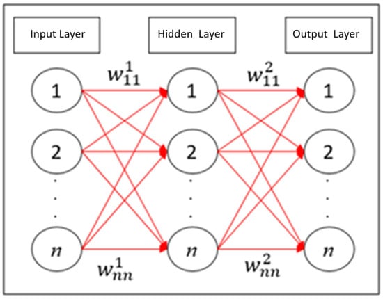
Figure 3.
Framework of BPNN.
The red lines in Figure 3 indicate that the BPNN model contains a large number of parameters. Therefore, this model performs extensive computations to generate accurate predictions. The process for weight update is performed in a backward manner, propagating from the data output layer to the hidden layer and then the data input layer. Partial differentiation of the loss function is conducted for to obtain the partial derivative Δ. At this point, the updated weight is expressed as − ηΔ, where η is the learning rate used to determine the magnitude of the partial derivative. The loss function is also used to obtain the partial derivative Δ concerning . However, considering that is not directly related to the loss function, the chain rule must be applied to perform the partial differentiation.
3.3. Random Forest
Ensemble learning is an algorithm that combines many base models to create a robust model, which outperforms individual models. Random forest (RF) [6] is an ensemble learning algorithm that integrates multiple decision trees to generate highly accurate predictions, making it a popular prediction model. A decision tree model is a conditional predictive model that partitions the output space of the data into k regions () based on the features and feature split points. Each of the k regions has a corresponding output value (), which is usually the average of the values within the region. Decision trees use different partitioning methods depending on the splitting approach. Common partitioning methods include classification and regression trees (CART), iterative dichotomiser 3, and C4.5. The present study adopted CART as the decision tree-splitting approach. Figure 4 shows a schematic diagram of CART, in which binary splitting is performed, with only one split conducted for each feature.
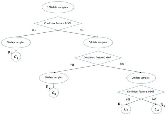
Figure 4.
Schematic diagram of CART.
In a decision tree, the quality of the feature split point determines the predictive capability of the model. Therefore, an indicator is required to evaluate whether the selected feature split point is appropriate. A common indicator is the impurity of the feature split point. The smaller the impurity, the greater the difference between the two groups of data after binary splitting, and the data partitioning becomes more effective. In regression problems, impurity is estimated using the mean square error (MSE).
where N represents the number of data points in the output space, and represents the average of the values in the output space.
In classification problems, impurity is often calculated using the Gini index, and the relevant equation is as follows.
where K represents the number of partitioned output regions.
An RF model uses a resampling method to expand the original data into M datasets. Each of the datasets is then input into a decision tree model to generate M decision tree models. Subsequently, the results of the M models are combined through majority voting or averaging to obtain the final result. An RF model is presented in Figure 5.
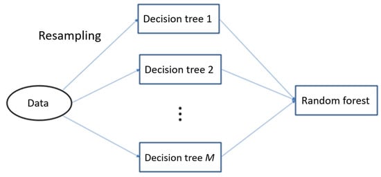
Figure 5.
Framework of RF model.
The resampling method used by an RF model ensures that the M datasets and their features are not identical. Therefore, the data diversity increases, which enhances the generalization capability of the model. The relationship between the output value and the input value of an RF model is expressed as follows.
where represents the output value (i.e., the predicted value) of the ith data sample, M denotes the number of decision trees, and K represents the number of output regions partitioned by each decision tree, is the output value of the region , and denotes an indicator function used to determine whether the ith data sample belongs to the output space , and that represents the features used by the ith data sample.
One advantage of an RF model is feature selection during the partitioning process; therefore, separate feature extraction need not be conducted to achieve good predictive performance. To improve computational efficiency, RF is used to evaluate the importance of features, thereby achieving more accurate computational results faster. Figure 6 illustrates the computational steps of an RF model.
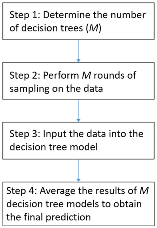
Figure 6.
Computational steps of RF model.
3.4. Data Description
Considering data completeness and usability, we focused on the PVD process of the Semiconductor Two-Dimensional Materials Laboratory at the Taiwan Instrument Research Institute. An energy consumption prediction model was established for the high-power impulse magnetron sputtering (HiPIMS) process at the laboratory. Details regarding the data source, data period, and other aspects are provided as follows.
- Data source: The data used in this study were collected by the HiPIMS monitoring system at the aforementioned laboratory. Figure 7 shows the interface of this system.
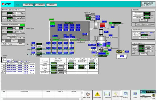 Figure 7. Interface of the HiPIMS monitoring system.
 - Data collection period: The data collection period was from 05:08 p.m. on 2 November 2021, to 09:42 a.m. on 11 May 2022.
- Number of records: A total of 115,942 records were collected in this study, and split into the training set (92,753 records, 80%) and testing set (23,189 records, 20%).
- Dependent variable (Y): The dependent variable was the HiPIMS power (W).
- Independent variables (X): The independent variables were the platform rotation speed (RPM), platform height (mm), chamber vacuum pressure (Torr), turbo pump vacuum pressure (Torr), cryopump vacuum pressure (Torr), heating temperature (°C), argon flow rate (sccm), power switch (ON/OFF), voltage (V), current (A), frequency (Hz), and pulse duration (µs).
- Modeling environment and programming language: The prediction models of this study were developed using the Jupyter web-based programming platform (jupyter_client: 8.6.1) and Python language (Python 3.10).
4. Comparison of Prediction Results of Different Models
MSE and convergence time were used to evaluate the performance of a polynomial regression model, a BPNN model, and an RF model in predicting the HiPIMS power (Table 1). The RF model exhibited considerably lower training and testing MSE values than the other two models. It required less time for convergence (training) than the other models. However, the average error rate of the RF model exceeded 5%, indicating that it can still be improved and refined.

Table 1.
MSE and convergence times of different models used to predict the HiPIMS power.
5. Conclusions
Three models were employed in this study to predict the HiPIMS power: a polynomial regression model, a BPNN model, and an RF model. Among these models, the RF model exhibited the lowest training and testing MSE values and the shortest convergence time. Therefore, this model was effective in predicting the energy consumption in HiPIMS. The developed RF model can be used to more accurately monitor the status of process equipment and systems when implementing energy-saving improvements in coating processes, thereby maximizing the overall benefits of such improvements. Although the developed RF model outperformed the other two models, its average error rate exceeded 5%, indicating room for improvement. In a future study, additional sensors need to be installed to collect essential data during HiPIMS. The collected data will serve as a crucial source for constructing accurate performance, yield, and energy consumption prediction models for the PVD coating process.
Author Contributions
Conceptualization, J.-H.W.; methodology, C.-W.C.; software, C.-Y.L.; validation, J.-H.W.; formal analysis, C.-Y.L.; investigation, C.-Y.L.; resources, C.-Y.L.; data curation, C.-Y.L.; writing—original draft preparation, J.-H.W.; writing—review and editing, J.-H.W. and C.-W.C.; visualization, J.-H.W.; supervision, C.-W.C.; project administration, J.-H.W.; funding acquisition, C.-W.C. All authors have read and agreed to the published version of the manuscript.
Funding
This research was funded by [National Science and Technology Council of Taiwan] grant number [NSTC 113-2224-E-492-001].
Institutional Review Board Statement
Not applicable.
Informed Consent Statement
Not applicable.
Data Availability Statement
The data is not publicly available due to confidentiality agreements.
Conflicts of Interest
All authors were employed by the company National Institutes of Applied Research and declare that the research was conducted in the absence of any commercial or financial relationships that could be construed as a potential conflict of interest.
References
- Liu, B.C.; Zheng, X.Y.; Weng, M.H.; Zhuang, S.Q.; Huang, L.X.; Li, J.C.; Wang, Y.M. Introduction to Precision Instruments; Canghai: Taichung City, Taiwan, 2014; Available online: https://www.sanmin.com.tw/product/index/004402858 (accessed on 28 August 2025).
- Smart Process System for Advanced Semiconductor Thin Film Equipment. Available online: https://itritoday.itri.org/110/content/en/unit_03-1.html (accessed on 1 September 2025).
- Yang, C.C. The Smart Manufacturing and Cyber—Physical Systems. Qual. Mag. 2021, 57, 29–32. Available online: https://www.airitilibrary.com/Article/Detail?DocID=10173692-202111-202112270020-202112270020-29-32 (accessed on 1 September 2025).
- Karsoliya, S. Approximating number of hidden layer neurons in multiple hidden layer BPNN architecture. Int. J. Eng. Trends Technol. 2012, 3, 714–717. [Google Scholar]
- Albelwi, S.; Mahmood, A. A framework for designing the architectures of deep convolutional neural networks. Entropy 2017, 19, 242. [Google Scholar] [CrossRef]
- Breiman, L. Random forests. Mach. Learn. 2001, 45, 5–32. [Google Scholar] [CrossRef]


Disclaimer/Publisher’s Note: The statements, opinions and data contained in all publications are solely those of the individual author(s) and contributor(s) and not of MDPI and/or the editor(s). MDPI and/or the editor(s) disclaim responsibility for any injury to people or property resulting from any ideas, methods, instructions or products referred to in the content. |
© 2025 by the authors. Licensee MDPI, Basel, Switzerland. This article is an open access article distributed under the terms and conditions of the Creative Commons Attribution (CC BY) license (https://creativecommons.org/licenses/by/4.0/).