
A Hardware Measurement Platform for Quantum Current Sensors †

 , , , , , and
Abstract
1. Introduction
1.1. Current Measurement
1.2. Nitrogen-Vacancy Centers
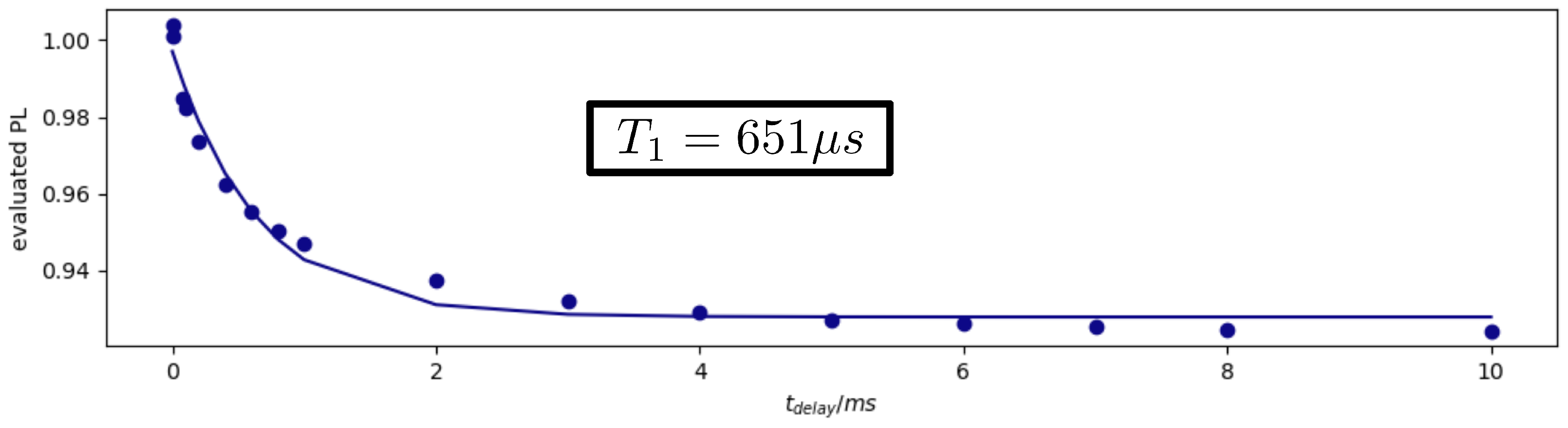
1.3. T1 Measurement
2. Methods
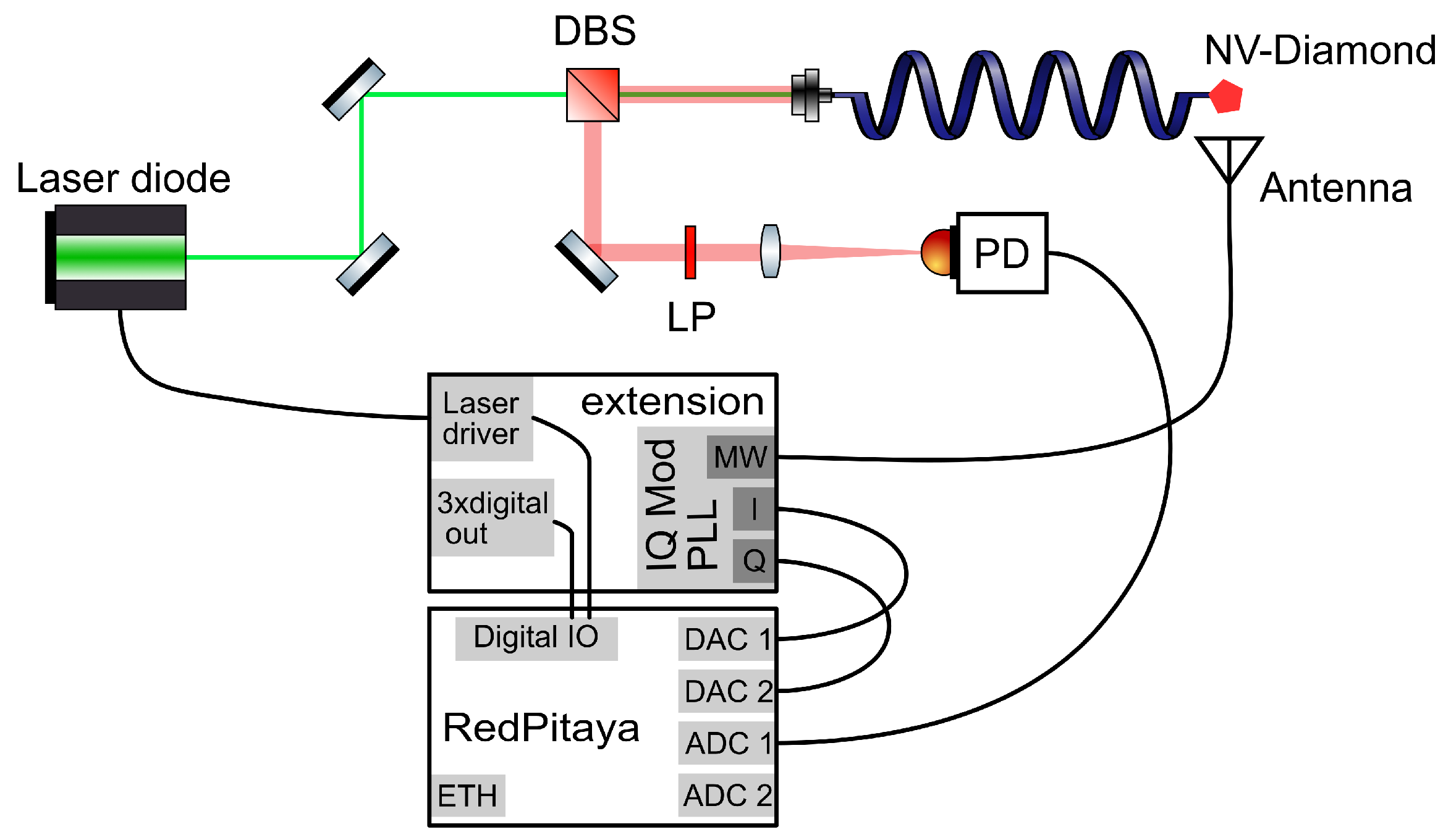
2.1. Optical Setup
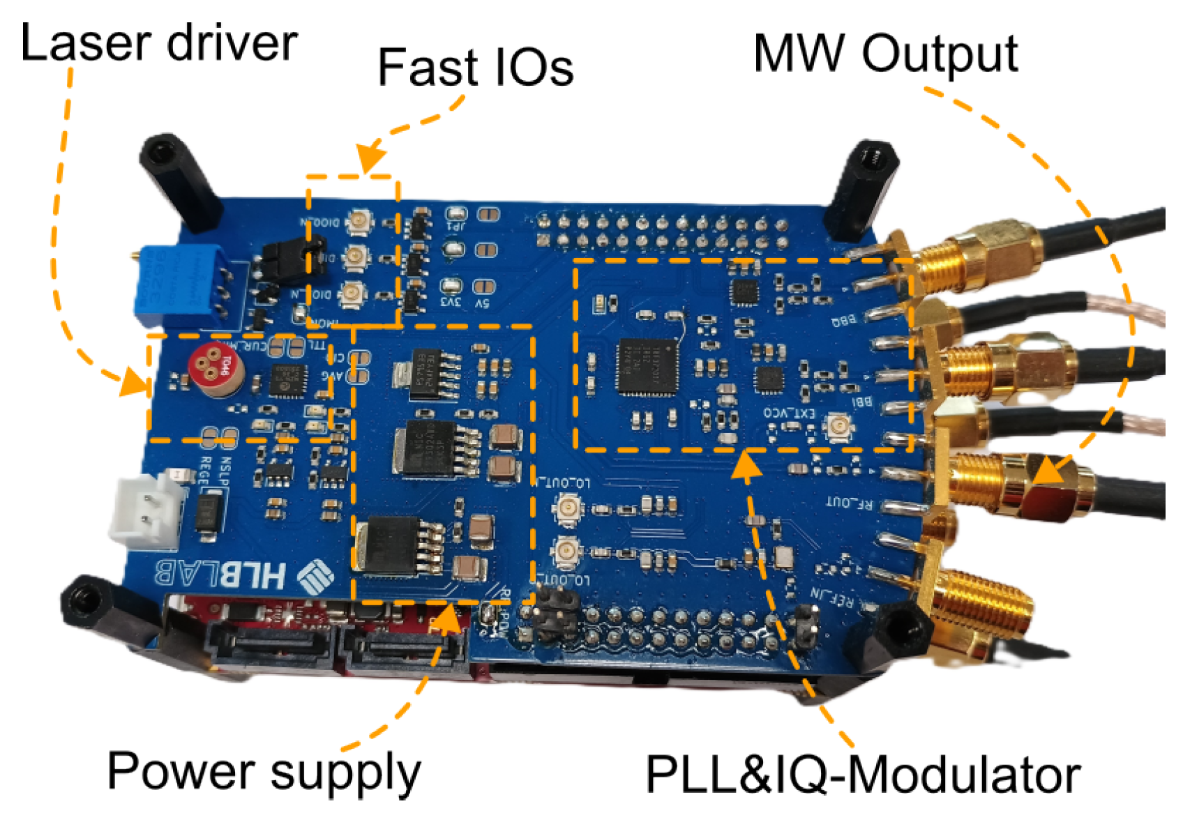
2.2. Electrical Setup
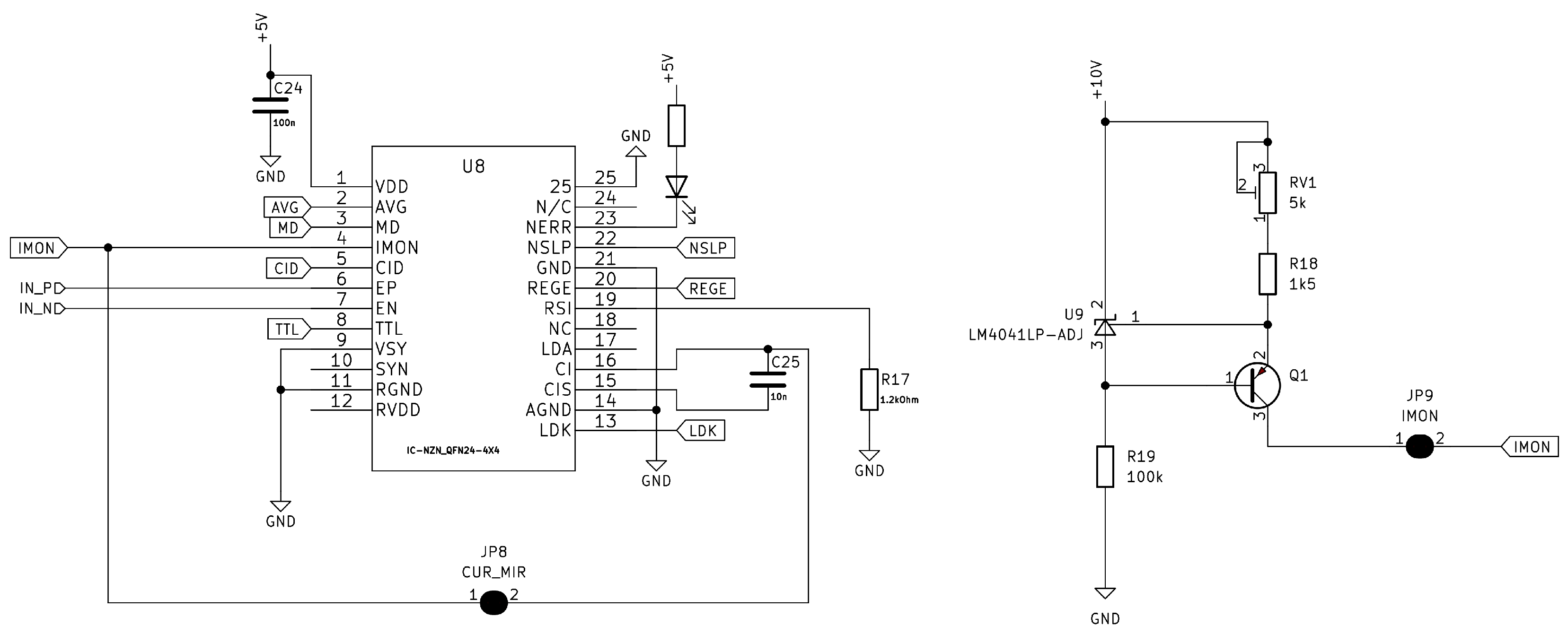
Laser Driver
3. Programmable Logic for T1 Measurement
3.1. Laser Pulse Generation
3.2. Data Acquisition and Measurement
4. Conclusions and Outlook
Author Contributions
Funding
Institutional Review Board Statement
Informed Consent Statement
Data Availability Statement
Acknowledgments
Conflicts of Interest
Abbreviations
| DBS | Dichroic Beam Splitter |
| FIFO | First In First Out |
| FPGA | Field Programmable Gate Array |
| MF | Multimode Fiber |
| MW | Micro Wave |
| NV | Nitrogen Vacancy |
| ODMR | Optically Detected Magnetic Resonance |
| PD | Photodiode |
| TCP/IP | Transmission Control Protocol/Internet Protocol |
References
- Crawford, S.E.; Shugayev, R.A.; Paudel, H.P.; Lu, P.; Syamlal, M.; Ohodnicki, P.R.; Chorpening, B.; Gentry, R.; Duan, Y. Quantum Sensing for Energy Applications: Review and Perspective. Adv. Quantum Technol. 2021, 4, 2100049. [Google Scholar] [CrossRef]
- Borle, S.Z.C.W.H.C.I.J. Current Sensing Techniques: A Review. IEEE Sens. J. 2009, 9, 354–376. [Google Scholar] [CrossRef]
- Pogorzelski, J.; Horsthemke, L.; Homrighausen, J.; Stiegekötter, D.; Gregor, M.; Glösekötter, P. Compact and Fully Integrated LED Quantum Sensor Based on NV Centers in Diamond. Sensors 2024, 24, 743. [Google Scholar] [CrossRef] [PubMed]
- Barry, J.F.; Schloss, J.M.; Bauch, E.; Turner, M.J.; Hart, C.A.; Pham, L.M.; Walsworth, R.L. Sensitivity optimization for NV-diamond magnetometry. Rev. Mod. Phys. 2020, 92, 015004. [Google Scholar] [CrossRef]
- Schloss, J.M.; Barry, J.F.; Turner, M.J.; Walsworth, R.L. Simultaneous Broadband Vector Magnetometry Using Solid-State Spins. Phys. Rev. Appl. 2018, 10, 034044. [Google Scholar] [CrossRef]
- Homrighausen, J.; Horsthemke, L.; Pogorzelski, J.; Trinschek, S.; Glösekötter, P.; Gregor, M. Edge-Machine-Learning-Assisted Robust Magnetometer Based on Randomly Oriented NV-Ensembles in Diamond. Sensors 2023, 23, 1119. [Google Scholar] [CrossRef] [PubMed]
- Neumann, P.; Jakobi, I.; Dolde, F.; Burk, C.; Reuter, R.; Waldherr, G.; Honert, J.; Wolf, T.; Brunner, A.; Shim, J.H.; et al. High-Precision Nanoscale Temperature Sensing Using Single Defects in Diamond. Nano Lett. 2013, 13, 2738–2742. [Google Scholar] [CrossRef] [PubMed]
- Acosta, V.M.; Bauch, E.; Ledbetter, M.P.; Waxman, A.; Bouchard, L.S.; Budker, D. Temperature Dependence of the Nitrogen-Vacancy Magnetic Resonance in Diamond. Phys. Rev. Lett. 2010, 104, 070801. [Google Scholar] [CrossRef] [PubMed]
- Schirhagl, R.; Chang, K.; Loretz, M.; Degen, C.L. Nitrogen-Vacancy Centers in Diamond: Nanoscale Sensors for Physics and Biology. Annu. Rev. Phys. Chem. 2014, 65, 83–105. [Google Scholar] [CrossRef] [PubMed]
- Jarmola, A.; Acosta, V.M.; Jensen, K.; Chemerisov, S.; Budker, D. Temperature- and Magnetic-Field-Dependent Longitudinal Spin Relaxation in Nitrogen-Vacancy Ensembles in Diamond. Phys. Rev. Lett. 2012, 108, 197601. [Google Scholar] [CrossRef] [PubMed]
- Dolde, F.; Fedder, H.; Doherty, M.W.; Nöbauer, T.; Rempp, F.; Balasubramanian, G.; Wolf, T.; Reinhard, F.; Hollenberg, L.C.L.; Jelezko, F.; et al. Electric-field sensing using single diamond spins. Nat. Phys. 2011, 7, 459–463. [Google Scholar] [CrossRef]
- Chen, E.H.; Clevenson, H.A.; Johnson, K.A.; Pham, L.M.; Englund, D.R.; Hemmer, P.R.; Braje, D.A. High-sensitivity spin-based electrometry with an ensemble of nitrogen-vacancy centers in diamond. Phys. Rev. A 2017, 95, 053417. [Google Scholar] [CrossRef]
- Shao, L.; Zhang, M.; Markham, M.; Edmonds, A.M.; Lončar, M. Diamond Radio Receiver: Nitrogen-Vacancy Centers as Fluorescent Transducers of Microwave Signals. Phys. Rev. Appl. 2016, 6, 064008. [Google Scholar] [CrossRef]
- Stürner, F.M.; Brenneis, A.; Kassel, J.; Wostradowski, U.; Rölver, R.; Fuchs, T.; Nakamura, K.; Sumiya, H.; Onoda, S.; Isoya, J.; et al. Compact integrated magnetometer based on nitrogen-vacancy centres in diamond. Diam. Relat. Mater. 2019, 93, 59–65. [Google Scholar] [CrossRef]
- Beaver, N.M.; Voce, N.; Meisenheimer, P.; Ramesh, R.; Stevenson, P. Optimizing off-axis fields for two-axis magnetometry with point defects. Appl. Phys. Lett. 2024, 124, 254001. [Google Scholar] [CrossRef]
- Sewani, V.K.; Vallabhapurapu, H.H.; Yang, Y.; Firgau, H.R.; Adambukulam, C.; Johnson, B.C.; Pla, J.J.; Laucht, A. Coherent control of NV-centers in diamond in a quantum teaching lab. Am. J. Phys. 2020, 88, 1156–1169. [Google Scholar] [CrossRef]
- Mrozek, M.; Rudnicki, D.; Kehayias, P.; Jarmola, A.; Budker, D.; Gawlik, W. Longitudinal spin relaxation in nitrogen-vacancy ensembles in diamond. arXiv 2015. [Google Scholar] [CrossRef]
- Hoffmann, F.; Bülter, A.S.; Horsthemke, L.; Stiegekötter, D.; Pogorzelski, J.; Glösekötter, P.; Gregor, M. Frequency Generation for a Quantum Current Sensor in Smart Grids. In Proceedings of the 2024 26th International Symposium on Symbolic and Numeric Algorithms for Scientific Computing (SYNASC), Timisoara, Romania, 16–19 September 2024; IEEE: New York, NJ, USA, 2024; pp. 341–343. [Google Scholar] [CrossRef]


Disclaimer/Publisher’s Note: The statements, opinions and data contained in all publications are solely those of the individual author(s) and contributor(s) and not of MDPI and/or the editor(s). MDPI and/or the editor(s) disclaim responsibility for any injury to people or property resulting from any ideas, methods, instructions or products referred to in the content. |
© 2025 by the authors. Licensee MDPI, Basel, Switzerland. This article is an open access article distributed under the terms and conditions of the Creative Commons Attribution (CC BY) license (https://creativecommons.org/licenses/by/4.0/).
Share and Cite
Hoffmann, F.; Bülter, A.-S.; Horsthemke, L.; Stiegekötter, D.; Pogorzelski, J.; Gregor, M.; Glösekötter, P. A Hardware Measurement Platform for Quantum Current Sensors. Eng. Proc. 2025, 101, 11. https://doi.org/10.3390/engproc2025101011
Hoffmann F, Bülter A-S, Horsthemke L, Stiegekötter D, Pogorzelski J, Gregor M, Glösekötter P. A Hardware Measurement Platform for Quantum Current Sensors. Engineering Proceedings. 2025; 101(1):11. https://doi.org/10.3390/engproc2025101011
Chicago/Turabian StyleHoffmann, Frederik, Ann-Sophie Bülter, Ludwig Horsthemke, Dennis Stiegekötter, Jens Pogorzelski, Markus Gregor, and Peter Glösekötter. 2025. "A Hardware Measurement Platform for Quantum Current Sensors" Engineering Proceedings 101, no. 1: 11. https://doi.org/10.3390/engproc2025101011
APA StyleHoffmann, F., Bülter, A.-S., Horsthemke, L., Stiegekötter, D., Pogorzelski, J., Gregor, M., & Glösekötter, P. (2025). A Hardware Measurement Platform for Quantum Current Sensors. Engineering Proceedings, 101(1), 11. https://doi.org/10.3390/engproc2025101011