Abstract
Photoanodes comprising a transparent glass substrate coated with a thin conductive film of fluorine-doped tin oxide (FTO) and a thin layer of a photoactive phase have been fabricated and tested with regard to the photo-electro-oxidation of water into molecular oxygen. The photoactive layer was made of a mat of TiO2 nanorods (TDNRs) of micrometric thickness. Individual nanorods were successfully photosensitized with nanoparticles of a metal–organic framework (MOF) of nickel and 1,2-benzene dicarboxylic acid (BDCA). Detailed microstructural information was obtained from SEM and TEM analysis. The chemical composition of the active layer was determined by XRD, XPS and FTIR analysis. Optical properties were determined by UV–Vis spectroscopy. The water photooxidation activity was evaluated by linear sweep voltammetry and the robustness was assessed by chrono-amperometry. The OER (oxygen evolution reaction) photo-activity of these photoelectrodes was found to be directly related to the amount of MOF deposited on the TiO2 nanorods, and was therefore maximized by adjusting the MOF content. The microscopic reaction mechanism which controls the photoactivity of these photoelectrodes was analyzed by photo-electrochemical impedance spectroscopy. Microscopic rate parameters are reported. These results contribute to the development and characterization of MOF-sensitized OER photoanodes.
1. Introduction
Water dissociation is the main route to the “hydrogen economy”, a human society in which hydrogen fuel could be produced efficiently and inexpensively from natural energy sources, without the need for fossil fuels [1]. Over the years, the dissociation of water into molecular hydrogen and oxygen by photo-electrolysis has emerged as a clean and sustainable technique for producing this eco-friendly and renewable hydrogen energy vector [2]. The dissociation of water in photoelectrochemical (PEC) cells is considered among the scientific community as a promising technique for the production of molecular hydrogen of electrolytic grade. From a historical perspective, the principles of photo-electrolysis were discovered as early as 1839 by Becquerel, the father of the photoelectric effect [3]. Another significant milestone was passed in 1973 when Fujima and Honda reported for the first time that n-TiO2 photoelectrodes operating in aqueous electrolytes could provide a significant fraction of the energy needed for direct water splitting [4]. From the economic viewpoint, the development of cost-effective, highly-efficient and long-term stable photo-electrocatalysts that could replace noble metal-based materials such as Pt, Ru, Au, and Ag used in water electrolysis cells is a prerequisite to bring the cost of electrolytic hydrogen down to market expectations [5,6]. The activity of a photo-electrocatalyst is usually dependent on, among other factors, material-related properties such as photo-absorbance, lifetime of photo-excited species, electrical conductivity and surface geometry of the electrode [7,8]. Hence, the requirements for enhancing PEC water-splitting performances are now well-established: these are to enlarge the light absorption range, to improve the separation and transfer of photoexcited electron–hole pairs, and to increase surface area. Semiconducting oxides have been thoroughly investigated. Their photoelectrocatalytic properties can be compared on the basis of these different criteria. Materials such as ZnO [9,10], CuxO [11,12], CeO2 [13,14], BiVO4 [15], WO3 [16] and TiO2-based nanomaterials are still considered as good photoactive semiconductors for water splitting. The positions of the conduction (CB) and valence (VB) bands in TiO2 adequately bracket the two redox potentials of the water dissociation reaction, which make these materials apt for PEC water splitting. Zhifeng et al. [17] successfully fabricated TiO2/BiVO4 photoelectrodes by using a simple spin-coating method, and reported photocurrents up to 35 µA cm−2 at 1.23 V vs. RHE under 100 mW cm−2 in 0.5M Na2SO4. Jeong et al. [18] reported the synthesis of vertically aligned ZnO-TiO2 core-shell nanorods (NRs), and this heterostructure displayed a photocurrent density about 2.41 times (1.23 mA cm−2) higher than pristine ZnO NWs. These studies not only proved that TiO2 is a candidate for effective photosensitizers, but also announced that suitable, well-ordered development of 1D structure with ideal semiconductors is key to amend the efficiency of PEC cells. Among a short list of potential candidates for application as substrate/catalyst in PEC cells and despite known limitations (TiO2 can absorb only a limited number of photons; morphological modification can improve its light absorption property, but it is owing to the light trapping effect, and by increasing the intrinsic property of the TiO2), TiO2 is almost the only suitable material for industrial use at present. Because of its cost-effectiveness, stability and efficient photoactivity, TiO2 has been recognized as an excellent noble-metal free photo-catalyst and has been widely used for that purpose [19,20]. In fact, the longest solar-to-hydrogen production record has been set using a TiO2 coated photocathode [21].
However, performance limitations remain such that new materials and innovative morphologies are still needed to increase the efficiency of the photon to hydrogen conversion, in order to envisage developments of practical interest. In particular, surface sensitization by functionalization of appropriate co-catalysts is required for the dual purpose of facilitating the absorption of visible light and enhancing the photon-to-hydrogen efficiency. Such combination of absorber/catalyst (which is required to increase stability and current density record) is now commonly used in state-of-art water splitting PEC cells [22,23]. Various types of photosensitizer/catalyst such as metal–organic frameworks (MOFs) can be used for that purpose. MOFs are compounds made of metal ions or clusters of metal ions, and bridging organic ligands, forming one-, two-, or three-dimensional structures. They form a subclass of coordination polymers having the characteristic of microporous architectures [24,25,26,27,28,29]. MOFs are porous solid materials having high surface area, a well-defined crystal pore structure, customizable chemical composition and structure, versatile functionality and improved biocompatibility [30]. Another interest of MOFs in view of electrochemical applications is that most of them contain transition metals (such as Fe, Co, Ni, Cu) combined with organic ligands containing C, H, O, N, S, P elements, which are all earth abundant and common elements in catalytic systems [31,32,33,34]. MOFs have already demonstrated that they are good photo-active materials for the oxygen reduced reaction (ORR), for environmental remediation, and for gas reduction due to their small band gap, excellent adsorption ability and porous structure [35,36,37,38]. MOFs are sometimes considered to be poor electrocatalysts for electrochemical reactions such as the OER and hydrogen evolution reaction (HER), two half-cell reactions involved in electrochemical water splitting [39]: some of them suffer from a lack of electrical conductivity and the size of the MOF crystallites is generally quite large (diameter generally greater than 1 μm), which limits their applications in electrochemical systems where nano-structuration is required to maximize the surface in contact with the electrolyte and to prevent fast recombination of charge carriers in bulk regions, before they can reach the surface. These two limitations are linked and can be circumvented either by finding a way to form particles or coatings of nanometric size, or by forming hybrid structures that make it possible to provide the necessary conductivity. Recently, an increasing number of techniques have been reported in the literature to fabricate MOFs and hybrid composites with controlled size, porosity and morphology, for various applications [28,40,41,42]. In order to increase the surface area and maximize the photo-response of MOF-containing photoelectrodes, many approaches have been tested to adapt the topography of MOF. For example, Zhan et al. [43] synthesized core-shell MOF heterostructures of ZnO@ZIF-8 nanorods, thus showing not only the interest of MOF fabrication but also the potential application of semiconductor@MOF heterostructures in many electronic devices. The transformation of traditional MOF nanocrystals into self-supporting and well-aligned MOF superstructures is highly desired for electrocatalysis but remains a significant challenge. Cai et al. [44] tried to solve the problem arising from the fact that the MOF particles are subject to aggregation during pyrolysis at high temperature, which leads to materials that are of reduced electronic conductivity and unsuitable for the transport of reagents and reaction products. They reported a versatile methodology for the controllable synthesis of three dimensional MOF hybrid arrays by using semiconducting nanostructures as self-sacrificing templates. They were thus able to keep the advantageous MOF superstructure and to prevent particles’ agglomeration, simultaneously. This result also demonstrated the successful fabrication of one-dimensional MOF array using a self-supporting growth method, and demonstrated their interest to the enhancement of water splitting performances.
Consequently, the development of nanostructures combining an oxide semiconductor of nanometric dimensions, coated on the surface with nanoparticles of photosensitizers, is still a very promising approach to obtain higher OER photoactivity. Based on these general considerations, we report here on photoelectrodes specifically designed for water photo-oxidation. Micrometric-thick mats of titanium dioxide nanorods (TDNRs) chemically grown on fluorine-doped tin oxide (FTO)/glass substrates have been successfully decorated with nanoparticles of a nickel-BDCA (benzene dicarboxylic acid) MOF. This Ni-MOF material was identified as a possibly good TiO2 photosensitizer and co-catalyst for the OER, because it can combine the known OER activity of Ni and high intrinsic porosity of MOF structures for electrolyte impregnation and mass transport to/from reaction sites. Individual TDNRs have been surface decorated by nanoparticles of Ni-BDCA MOF using a two-step process, the electrodeposition of nanoparticles of nickel hydroxide followed by their chemical transformation into Ni-BDCA MOF using a simple hydrothermal procedure after the addition of organic ligands. Regarding the electrodeposition step, cyclic voltammetry has been used instead of chronopotentiometry or chronoamperometry to form uniform coatings of controllable shape and thickness over the TiO2 surface. The photosensitizing effect of the MOF and the increased OER photoactivity resulting from the MOF have been put into evidence by using linear sweep voltammetry, chrono-amperometry, and photo-electrochemical impedance spectroscopy. A superior OER photo-activity has been obtained with these novel Ni-BDCA/TDNRs/FTO/glass photoanodes, showing promising interest for water splitting in PEC systems.
2. Materials and Methods
2.1. Chemicals
All the chemicals used in this work were of analytical quality. Milli-Q quality water (18.2 MΩ cm) was used in all experiments. Titanium tetrachloride (98%), nickel (II) nitrate hexahydrate (98%), 1,2- benzene dicarboxylic acid (98%) were purchased from Alfa Aesar (Kandel, Germany). The electrolytic solution was prepared by using Sodium sulfate (≥99.0%) from Sigma-Aldrich (Saint-Quentin Fallavier, France). HCl (36%), N, N-Dimethylformamide (anhydrous, 99.8%), Methanol (≥99.9%) and washing solvent (Ethanol, 2-propanol and acetone) were all purchased from VWR (Fontenay-sous-Bois, France).
2.2. Fabrication of TDNRs/FTO/Glass Photoelectrodes
Several photoelectrodes made of FTO-covered glass substrates (Solaronix Co. Ltd., Aubonne, Switzerland) have been prepared. The mats of TiO2 nanorods have been synthesized chemically using a cylindrical autoclave made of stainless steel lined with an internal Teflon wall [2,45]. In a typical experiment, a piece of transparent FTO/glass electrode (1.3 cm × 2.5 cm) was previously cleaned for 30 min in an ultrasonic bath containing a mixture of water-isopropanol- acetone (1:1:1), then air-dried at room temperature. An active area of 1 cm2 was then delimited using Teflon tape. The solution used for the hydrothermal treatment and the growth of TiO2 nanorods was prepared as follows. First, 60 mL of a solution of hydrochloric acid (36%) in deionized water (1:1 volume ratio) was prepared. Then, 1 mL of titanium (IV) n-butoxide was added and the mixture was stirred for 10 min. Then, the FTO/glass piece was placed inside the autoclave against the wall, and the vessel was filled with the solution, then sealed and heated at 150 °C for 4 h in a drying oven. After reaction, the container was cooled to room temperature in ambient air. Subsequently, the electrode was removed from the autoclave, thoroughly washed with deionized water and finally air-dried at room temperature.
2.3. Electrodeposition of Ni Species onto the TDNRs/FTO/Glass Photoelectrodes
Nickel was electrodeposited over the TDNRs mats using a conventional three-electrode electrochemical cell. The cell was equipped with an Ag/AgCl reference electrode (RE), a glassy carbon plate used as counter electrode (CE) and the TDNRs/FTO/glass photoelectrodes used as working electrode (WE). First, the as-prepared TDNRs/FTO/glass electrodes were immersed into 40 mL of freshly prepared Ni(NO3)2·6H2O solutions of various concentration (0.001 M~0.1 M). Second, the nickel was electrodeposited by cyclic voltammetry, by cycling the potential of the WE over the −0.2V to −1.0 V potential range at a scan rate of 10 mV/s, for a different number of cycles (referred to as 2C, 5C, 10C). Finally, after Ni deposition, the photoelectrodes were rinsed three times with deionised (DI) water and dried in air at ambient temperature.
2.4. Formation of the Ni-BDCA MOF onto the TDNRs/FTO/Glass Photoelectrodes
Finally, the Ni coatings were chemically transformed into Ni-BDCA MOF by addition of the organic ligands of the target MOF in the Teflon-lined stainless-steel autoclave. Briefly, 1,2-benzene dicarboxylic acid (BDCA) was dissolved into a mixture of methanol (MeOH) and DMF (1:9 vol. ratio) under continuous stirring for 1 hr to form a 5 g/L (0.03 M) solution. In a typical experiment, the Ni/TDNRs/FTO/glass photoelectrode was placed face-up in the vessel and covered with the BDCA solution. The autoclave was then sealed and heated at 150 °C for 4 h. After that, the photoelectrode was cooled to ambient temperature in air, washed three times with DI water and absolute ethanol and finally dried at 60 °C for 1 h. Additionally, the Ni-BDCA MOF was synthesized by using 1M Ni(NO3)2·6H2O solutions with same ratio of BDCA/DMF/MeOH solution via hydrothermal under 150 °C for 4 h. The suspension was collected and centrifuged three times by washing with ethanol, and the powder was obtained by heating under 60 °C overnight.
2.5. Physical Characterization
A scanning electron microscope (FEG-SEM, ZEISS Sigma HD, Oberkochen, Germany; 1–2 kV acceleration voltage in high vacuum mode), was used for investigating the surface morphologies of the different samples. Elemental analysis was performed in-situ by energy dispersive X-ray (EDX) spectroscopy analysis, using an analyzer (SAMx IDfix, Lavardens, France) placed on the SEM, operating with an acceleration voltage of 15 kV. An X-ray diffractometer (x’pert pro, PANalytical, Malvern, United Kingdom) with CuKα radiation (wavelength λ = 1.54045 Å) operating at an accelerating voltage of 40 kV and a current of 35 mA, was used to record DRX spectra in the 5–80° range and to identify the crystallite phases and structure of TDNRs, and Ni-MOF/TDNRs. The chemical states of the different elements were determined by X-ray photoelectron spectroscopy (XPS) analysis, using a Kα, Thermo Fisher Scientific analyzer equipped with a monochromatic aluminum source (Al Kα, 1486.68 eV). All measurements have been made in an ultra-high vacuum (UHV) chamber, at a residual pressure of less than 10−9 mbar. A 400 µm diameter spot corresponding to an irradiated area of approximately 1 mm2 was used for the measurements. The hemispherical analyser operated at a take-off angle of 0° in CAE (Constant Analyser Energy) mode, with a passing energy of 200 eV (and an energy step of 1 eV) for the acquisition of wide scans, against a passing energy of 50 eV (and an energy step of 0.1 eV) for the acquisition of spectra over narrower energy ranges. The charge compensation was carried out by means of a double flow gun, using low energy electrons (5 eV) and argon ions. Samples were fixed to the support using adhesive and conducting tape. The recorded spectra were processed using the Avantage software, using a peak adjustment routine with a Shirley background and mixed Gaussian–Lorentzian peak shapes (70%–30%). The atomic ratios were evaluated after normalizations of the peak areas with the Scofield sensitivity factors. The optical properties of the different samples were measured using a Cary 60 UV–vis spectrophotometer (Agilent, Santa Clara, CA, USA). Reflection and absorption mode experiments were performed, using an FTO uncoated glass piece as a reference for removing the background.
2.6. Photo-Electrochemical Measurements
The photoelectrochemical properties of the photolectrodes were measured in a three-electrode cell equipped with a quartz window (Pine Research Instrument Company, Durham, NC, USA), using a ModuLab XM potentiostat (Solartron, Farnborough, United kingdom). The measurements were carried out using the photoelectrodes as working electrodes, a counter electrode (high surface area Pt wire), and a reference electrode (Ag/AgCl electrode). A 0.1 M Na2SO4 solution (pH~6.5) was used as the liquid electrolyte. Alphagaz 2 grade argon was bubbled through the electrolyte for 30 min before starting the measurements to remove dissolved air. To avoid contamination of the electrolyte during the measurements, an atmosphere of argon was maintained on the surface of the electrolyte during all the experiments. The working photoelectrode was then illuminated using a solar simulator (Asahi Spectra Co., MAX-303, Torrance, CA, USA) equipped with a 300 W xenon lamp. The light intensity of the simulated light was adjusted in order to apply the equivalent of 1 sun (100 mW cm−2) on the surface of the working photoelectrode. Linear Scanning Voltammetry (LSV) was used to record voltammograms at 10 mV s−1, over the potential range from −0.6 to +1.2 V vs. Ag/AgCl, in the dark and under chopped lighting. Chronopotentiometric measurements were carried out at a constant potential of +1 V relative to Ag/AgCl, under chopped and continuous lighting. The photoelectrochemical impedance spectroscopy (PEIS) spectra were recorded under different lighting conditions (Uv–vis, Visible and in the dark), over a range of potentials ranging from −0.6 to +1.2 V vs. Ag/AgCl, over the frequency range 100 kHz to 50 mHz, using an AC modulation voltage of 10 mV amplitude. The Mott–Schottky curves were recorded at a constant frequency of 10 Hz over the potential range from −1.0 V/+1.0 V vs. Ag/AgCl.
3. Results and Discussion
3.1. Structural and Morphological Characterization
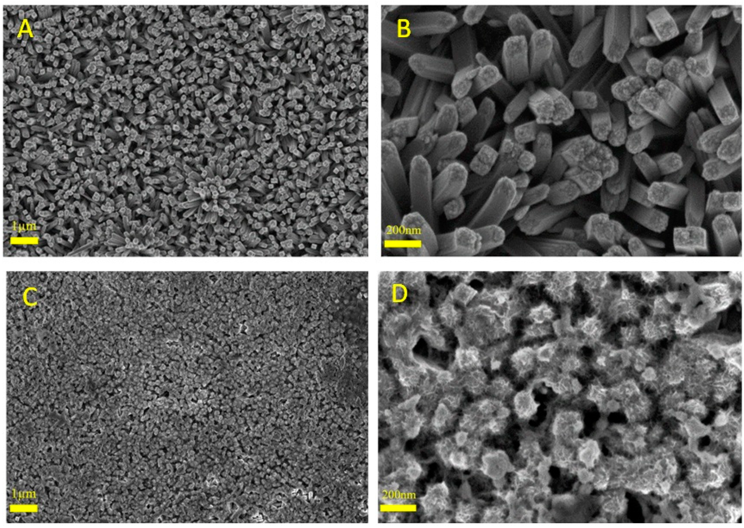
Figure 1 shows the SEM images of a typical active layer taken before and after the deposition of the MOF. Those of the naked TDNRs (Figure 1A,B) taken, respectively, with a low and high magnification) clearly show the structure of the TiO2 mat. The deposit consists of aligned nanorods of micrometric length. The individual TiO2 nanorods are tetragonal in shape and their diameter is approximately 100 nm. Figure 1C shows an overview of the mat after the formation of the nickel MOF. A closer examination of the microstructure (Figure 1D) confirms the presence of the Ni-MOF coating on the TDNRs mat. In this example, the amount of MOF is sufficient to cover each individual TiO2 nanorod with Ni-MOF crystals. Empty spaces are observed between these rods, opening the way for electrolytic impregnation. However, the MOF coating does not consist of isolated nanoparticles: it is a thin film covered with spines of nanometric size, resulting from the germination–growth process. Compared to the structure of the naked rutile phase of TDNRs, such nanostructuring is very interesting and seems appropriate for increasing the porosity and the active surface of contact with the electrolyte, in order to favour the absorption of light and the separation of charges. Such nanoarchitectures are highly desirable for enhancing the intrinsic activity of the compounds for OER.
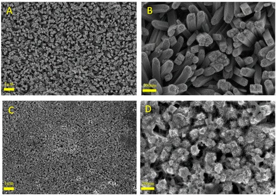
Figure 1.
SEM images of (A,B) bare titanium dioxide nanorods (TDNRs), and (C,D) 0.005 M-2C-Ni-MOF/TDNRs.
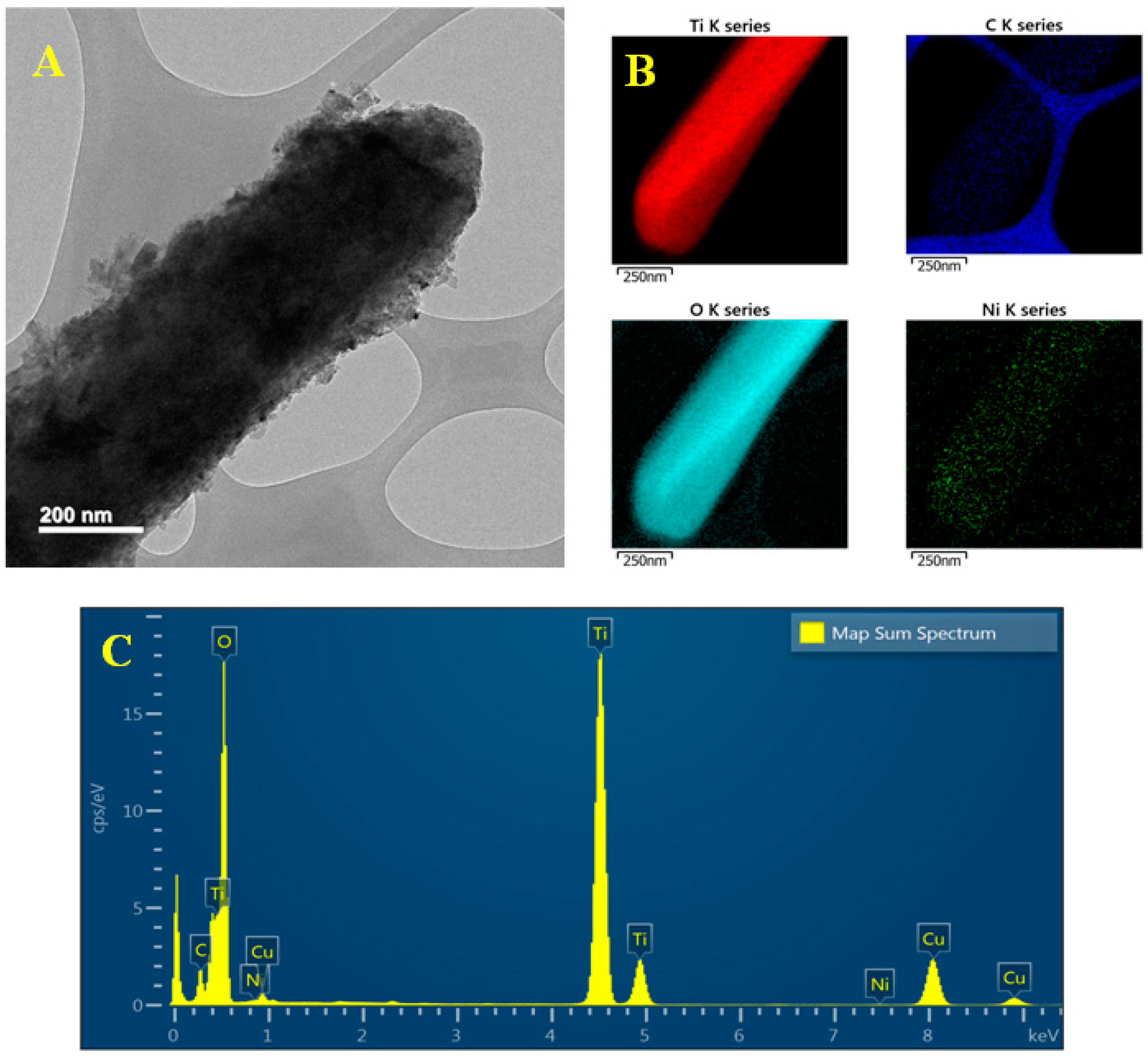
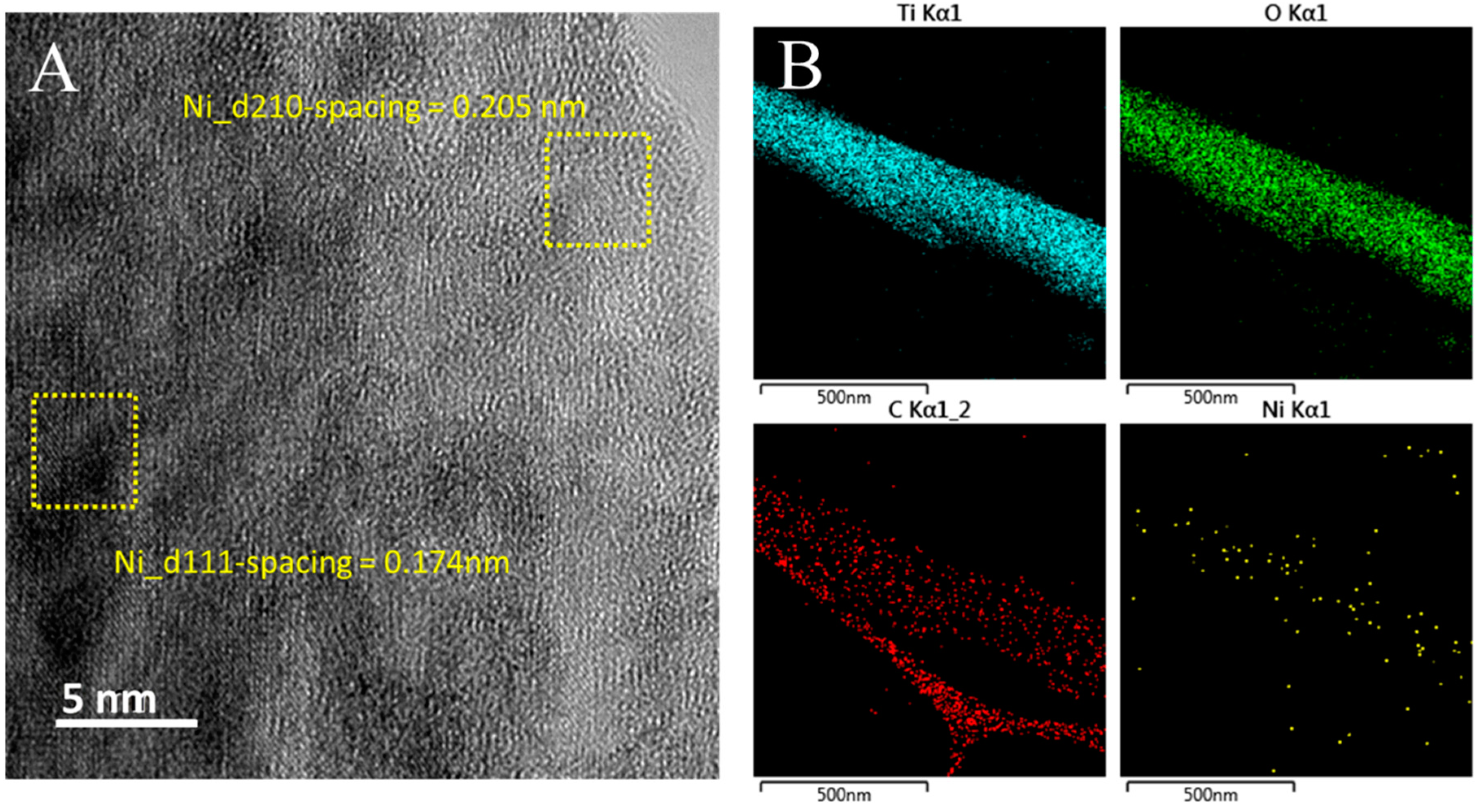
Figure 2A shows the HRTEM image of an individual Ni-MOF/TDNR (the sample observed here is the one prepared using the 0.005 M Ni solution). The TDNRs are homogeneously covered by a 50 nm thick Ni-MOF coating, a thickness value in good agreement with the SEM results. Figure 2B,C show, respectively, the elemental cartography and the EDX spectrum of the nanorod shown in Figure 2A. It is found that nickel (green color) and carbon (blue color) are homogeneously distributed over the entire surface of the TiO2 nanorod (red and cyan colors). The spectrum of Figure 2C indicates that the percentage of Ni is approximately 0.03 % only, while the Ti percentage is close to 30% for the 0.005 M-2C-Ni-MOF/TDNRs sample. The conclusion of these observations is that TiO2 is homogeneously covered by Ni-MOF. The quantity of electrodeposited nickel is low compared to TiO2: only the extreme surface of the wires is sensitized, as desired. The lattice texture of Ni-MOF/TDNRs has also been investigated. The interplanar spacing of the lattice fringes measured in different regions of a single nanoparticle is found to be different (Figure 3A). In the fringe (interplanar) spacing calculated from the FE-TEM image by Digital Micrograph (Gatan Inc., Warrendale, PA, USA), the lattice distances are found to be approximately 0.17 nm and 0.20 nm, corresponding, respectively, to the (200 (XRD = 45.7°)) and (111 (XRD = 43.5°)) lattice planes of NiO [46]. Such results suggest that NiO clusters form the center of Ni-MOF coatings, as discussed elsewhere [47,48]. This was also observed on XPS and FTIR spectra. Unfortunately, the d110-spacing of 1.1 nm, referring to carbon species, is not showing on the lattice fringes and is also not clear in XRD pattern, but can still be easily observed on the graphs of elements mapping analysis and the XPS spectra. In Figure 3B, the elements mapping shows the Ni species homogeneous separately constructed with carbons and attached on single TiO2 rod. It is clear that the Ni-MOF successfully grows on each rod of TDNRs’ surface.

Figure 2.
(A) HRTEM image and (B,C) elemental EDS mapping diagram of 0.005M-2C-Ni-MOF/TDNRs.
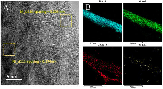
Figure 3.
(A) The interplanar spacing image and (B) elemental mapping diagram of 0.005M-2C-Ni-MOF/TDNRs obtained by FETEM analysis.
To increase the amount of Ni-MOF deposited on the surface of the TiO2 nanorods, it is possible (i) to increase the concentration of the nickel solution used in the preparation or (ii) to increase the number of cyclic voltamograms used to deposit nickel on the surface (see experimental section for details). Typical results are shown in Figure 4. As the number of cyclic voltammograms increases, the surface of the individual TiO2 nanorods gradually becomes coated with increasing Ni-MOF coating. After coating, the diameter of individual nanorods is increased, as logically expected. There is also a change in coating morphology. The SEM images of Figure 4A,C,E, show the prevailing situation when a diluted (5 × 10⁻³ M) Ni solution is used and the number of cycles (2, 5 and 10, respectively) is increased. The amount of Ni-MOFs gradually increases and the diameter of the MOF-decorated nanorods increases from 100 nm (0 cycle) to 200 nm (2 cycles) and up to 500 nm (10 cycles). When a more concentrated Ni solution is used (0.01 M instead of 5 × 10⁻³ M), the growth is faster, indicating that the kinetics of nickel deposition is controlled by mass-transport of nickel ions in solutions. After 10 cycles, the surface is almost totally covered by a thick and continuous Ni-MOF layer (Figure 4F). The EDX spectra measured on the different samples (Figure S1, Supporting Information) clearly show the presence of Ti and O peaks related to TiO2 nanorods over the FTO surface. Nickel peaks of increasing intensity are also seen after MOFs deposition. However, these peaks are of low intensity because the quantity of MOF deposited is low and because the EDX detector has limited sensitivity. EDX alone cannot tell which species of nickel have been deposited. During the photoelectrochemical tests (see details in the following sections), it was observed that the initial thickness and arrangement of the Ni-MOF coating/layer over the TiO2 nanorods were the two main factors which affect the concentration of photo-reactive sites and hence the charge transfer kinetics. We can deduce that the best photoelectrochemical performances are obtained by increasing the number of 1D reaction sites, in order to accumulate photo-generated electrons at the top of the rods. The best structure leading to the highest OER photoactivity was obtained after only two nickel deposition cycles. A limited but nevertheless appropriate amount of Ni-MOF was deposited under these conditions, thus reducing the shielding effect and contact impedance at the interface between the Ni-MOF coating and the TDNRs.
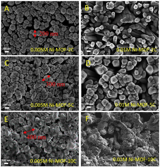
Figure 4.
SEM images of different Ni-MOF/TDNRs samples: (A) 0.005 M-2C, (B) 0.01M-2C, (C) 0.005 M-5C, (D) 0.01M-5C, (E) 0.005 M-10C, (F) 0.01M-10C.
3.2. Physico-Chemical Characterization
XRD analysis was first used to characterize the crystal structure of the synthesized Ni-MOF/TDNRs samples. As shown in Figure 5A, the FTO diffraction pattern is clearly visible before and after MOF deposition. There is also a good agreement between the XRD spectrum measured on the reference sample (TDNRs without MOF) and the calculated spectrum of TiO2, which confirms the successful growth of TDNRs over the FTO/glass substrates. The diffraction peaks measured on the TDNRs/FTO sample appear for values of 2θ equal to 27.40°, 36.04°, 41.20°, 43.90°, 62.60°, 68.80° and 69.80°, corresponding to the diffraction planes (110), (101), (111), (210), (002), (301), and (112), respectively (PDF No.98-000-0090). The diffraction pattern measured on the Ni-MOF/TDNRs/FTO sample is very similar to the diffraction pattern measured on the TDNRs/FTO sample. However, there is no clearly additional peak indexed to Ni-MOF and the diffraction features of the coating. As shown in Figure S2 (Supporting Information), the experimental XRD patterns of Ni-MOF, synthesized by higher concentration, show sharp peaks that matched well with the XRD patterns already reported in the literature [49], and no additional peak is observed, which demonstrates that the synthesized Ni-MOF phase is pure and monophasic. However, despite the higher amount of Ni-MOF loading on TDNRs, there is still no sharp peak observed for Ni-MOF in the XRD profiles.
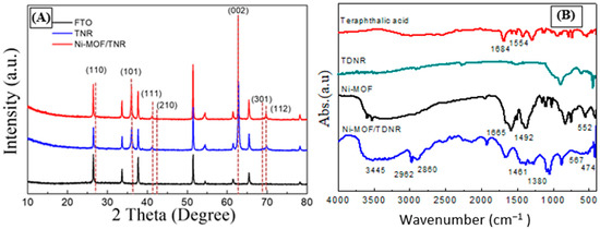
Figure 5.
Physical characterization of the TDNRs and Ni-MOF/TDNRs samples on FTO glass: (A) XRD pattern of FTO, TDNR and 0.005M-2C-Ni-MOF/TDNR, (B) FTIR spectra of BDCA, TDNR, Ni-MOF, and 0.005M-2C-Ni-MOF/TDNRs.
Figure 5B shows the experimental absorbance spectrum of the Ni-MOF/TDNRs and TDNRs obtained by FTIR in the range of 400–4000 cm−1. Yang G. et al. reported a FTIR spectrum of similar shape and band structure for the BDCA: the IR spectrum of Ni-MOF also covers an absorption band at 2860–2962 cm−1. The absorption band was attributed to the CH stretch vibration of CH3 and CH2. The strong absorption peaks at 1461 cm−1 and 1380 cm−1 correspond to the CH bending vibration of CH3 and CH2, respectively. Additionally, there is another strong absorption peak emerging at 1665 cm−1, which is a bit lower than the stretching vibration value of C=O of BDC (1684 cm−1) [50]. The shift has been attributed to the deprotonation of the carboxylic acid group. Differing from BDC, Ni-MOF show an absorption band of thioureide around 1492 cm−1, and this band blue shifts to some extent as compared with the thioureide band of BDC at 1554 cm−1. The bond can be reckoned as an intermediate between (CN) single bond and (CN) double bond and it implies metal coordination due to the delocalization of electrons resulting in a partial double bond character [51]. Additionally, an apparently board peak of Ni-MOF and Ni-MOF/TDNRs observed at 3445 cm−1 can be assigned to the bending vibration of –OH or H2O on the photocatalyst, and the peaks of Ni-MOF/TDNRs appear at 474 and 567 cm−1 in the spectrum, which was attributed to the Ni-O stretching vibrations. The two peaks indexed to NiO also represented of the Ni-MOF spectra at 552 cm−1 [52]. The broad absorbance peak for TDNRs is situated at 1066 cm−1 and is indexed to Ti-O bonding [53]. The FTIR data confirmed the components of Ni-MOF/TDNRs, and illustrated the same description as that observed under FETEM.
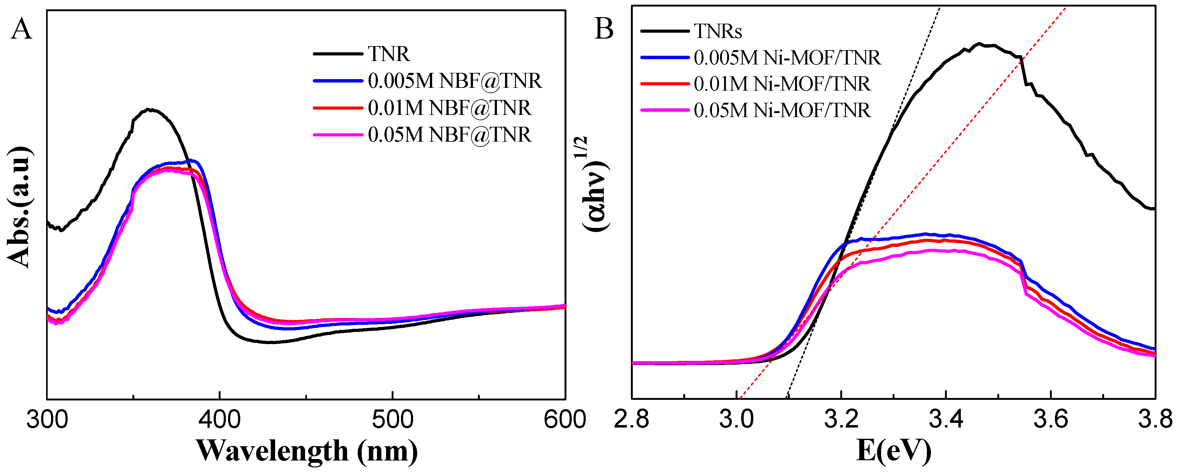
UV–Vis absorption spectroscopy has been used to measure the optical properties of the different samples. UV–Vis spectra in diffuse reflectance mode (DRS) were measured; results are shown in Figure 6A. Compared to the bare-TiO2 sample, the absorption spectra of the different samples containing MOF are shifted by approximately 10–15 nm towards the visible range. The intensities of the absorption peaks measured on the various samples containing MOF are proportional to the amount of MOF deposited. At 390 nm, the absorption intensity increases while the amount of Ni-MOF is decreased, which also reveals the ability of visible light absorption of Ni-MOF/TDNRs while operated under PEC system. The band gap energies of the four different samples were calculated from the Tauc plots (Figure 6B) using the Kubelka–Munk formula. In the linear zone of the plots, the relationship that must be satisfied is expressed according to Equation (1):
where Eg is the band gap energy, hυ is the photon energy, α is the absorption coefficient, h is the Planck’s constant, υ is the photon frequency and K is the proportionality constant. The optical band gap energies Eg of the different Ni-MOF/TDNRs samples were determined by extrapolating the tangent lines to the steep parts of the Tauc plots in the high energy range to the hν axis. The absorption data were fitted for both indirect and direct allowed band gap transitions. A satisfactory fit for the allowed indirect transitions was obtained for all of the samples. The band gaps were found to be between 3.0 and 3.1 eV (Figure 6B). By increasing the amount of Ni-MOFs deposited onto the TDNRs mats, an energy shift towards visible light was observed. This reduction in the band energy is limited but puts into evidence the photosensitizing effect resulting from the addition of Ni-MOF onto the TDNRs mats.
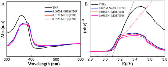
Figure 6.
Optical characterization of TDNRs and TDNRs modified with different amounts of Ni-MOF after 2 cycles of electrodeposition by CV method. (A) UV–Vis diffuse reflectance spectra and (B) Tauc plots.
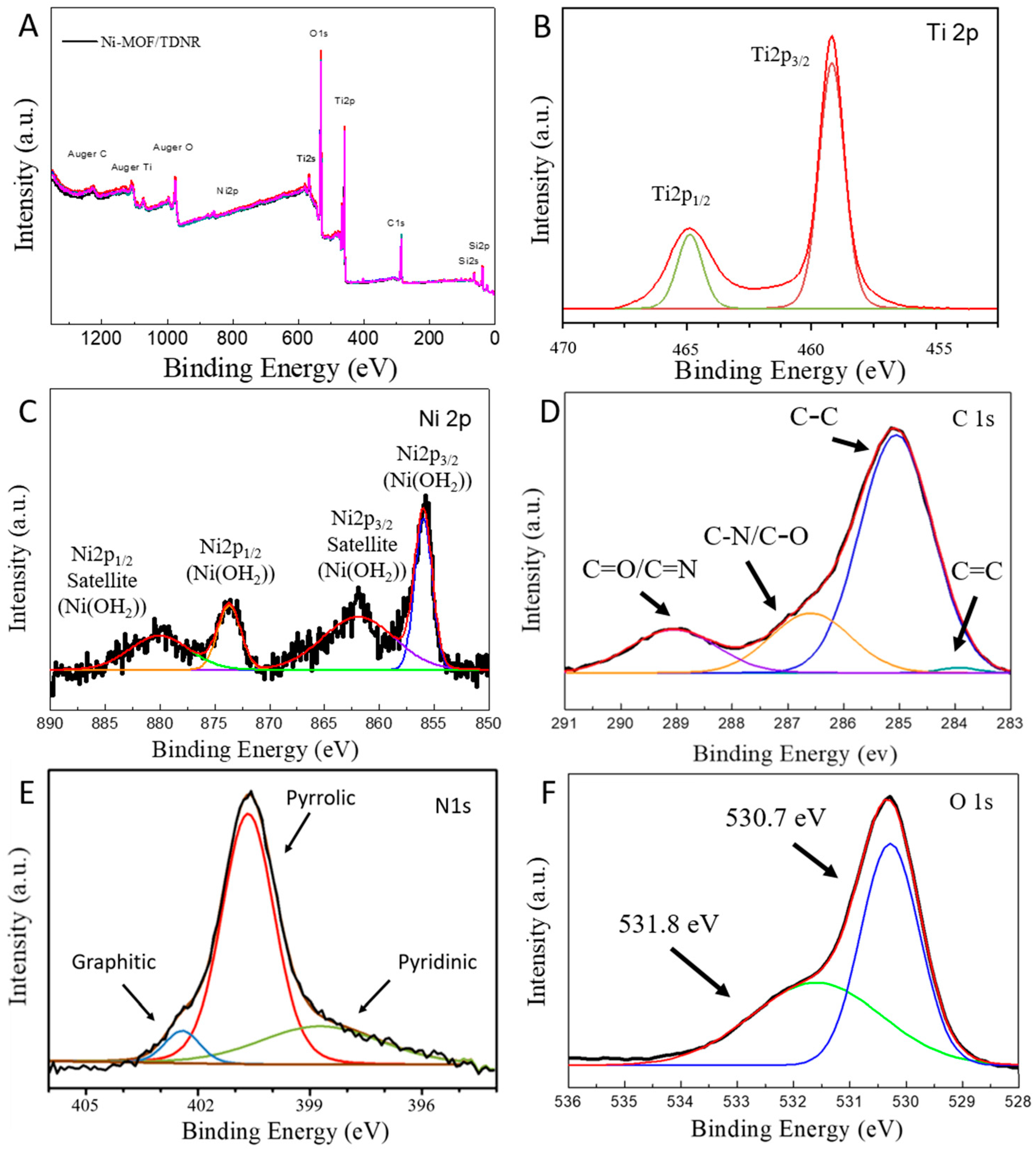
XPS analysis was performed to determine the chemical composition of the coating at the extreme surface in contact with the electrolyte, and to demonstrate that the Ni-MOF/TDNRs electrodes were successfully synthesized. Figure 7A shows an overview of the XPS spectrum measured on the 0.005M-2C-Ni-MOF/TDNRs sample. The different elemental peaks are indexed. Five survey spectra, measured at five different locations over the surface of the photoelectrode are plotted together. They are the same, indicating that the surface is chemically homogeneous. Experimental and calculated XPS spectra of Ti 2p, Ni 2p, C 1s, N 1s, and O 1s are shown in Figure 7B–F, respectively. In Figure 7B, the Ti spectrum contains two main peaks centered at approximately 465.2 eV and 459.5 eV. They are attributed to Ti 2p1/2 and Ti 2p3/2. Their presence indicates that a TiO2 nanostructure was formed [54]. The situation prevailing for nickel is shown in Figure 7C. Two main peaks positioned at 856.1 and 873.6 eV are observed. They are assigned to Ni 2p3/2 and Ni 2p1/2, together with their corresponding satellite peaks located at 861.7 and 880.6 eV. Such spectra are characteristic of a Ni (OH)2 phase.
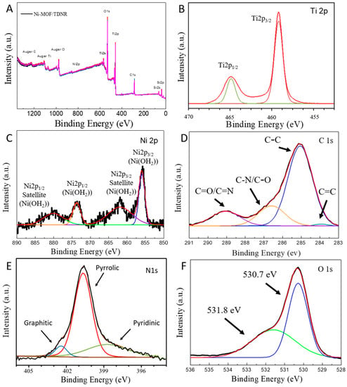
Figure 7.
XPS spectra measured on the 0.005M-2C Ni-MOF/TDNRs: (A) overview; (B) Ti 2p; (C) Ni 2p; (D) C 1s; (E) N 1s; (F) O 1s experimental and fitting results.
By analyzing the carbon (C1s), nitrogen (N1s) and oxygen (O1s) contributions (Figure 7D–F), it was possible to conclude that the expected MOF structure was formed.
The carbon sp2 peak of C=C/C=N and C-C/C-N shows the aromatic ring of BDCA compounds link with DMF substances. Moreover, the three N peaks were indexed to graphitic (402.5 eV), pyrrolic (400.5 eV) and pryridinic (398.5 eV) nitrogen components, respectively. According to FTIR and XPS results, all the evidences suggests that BDCA and DMF form the [(BDCA) (DMF) (MeOH)]n complex and combined with the NiO cluster to form the targeted MOF architecture. In order to compare the Ni (OH)2/TDNRs and Ni-MOF/TDNRs, the XPS spectra of the Ni (OH)2/TDNRs as represented in Figures S3 and S4 (Supporting Information). The peaks of Ni and Ti are relative sharp and fit well with Ni (OH)2 and TiO2 by software (Casa XPS) compared to the one in Ni-MOF/TDNRs, and it is clear that the small peaks of carbon (C1s) and nitrogen (N1s) in sp2 state are different, which may index to residues of solvent and nitrate substrate. Furthermore, in the detail of the XPS spectra for Ni (OH)2 deposited on TDNRs and Ni-MOF/TDNRs is shown in Figure S4 (Supporting Information). Ni-MOF exhibits a Ni 2p spectrum which is quite similar to Ni(OH)2, which is also composed of two main peaks, along with two satellite peaks. However, all the Ni 2p peaks measured on Ni-MOF are noticeably shifted to higher binding energies, which related to the satellite peak of the case of Ni or NiO.
3.3. PEC Analysis
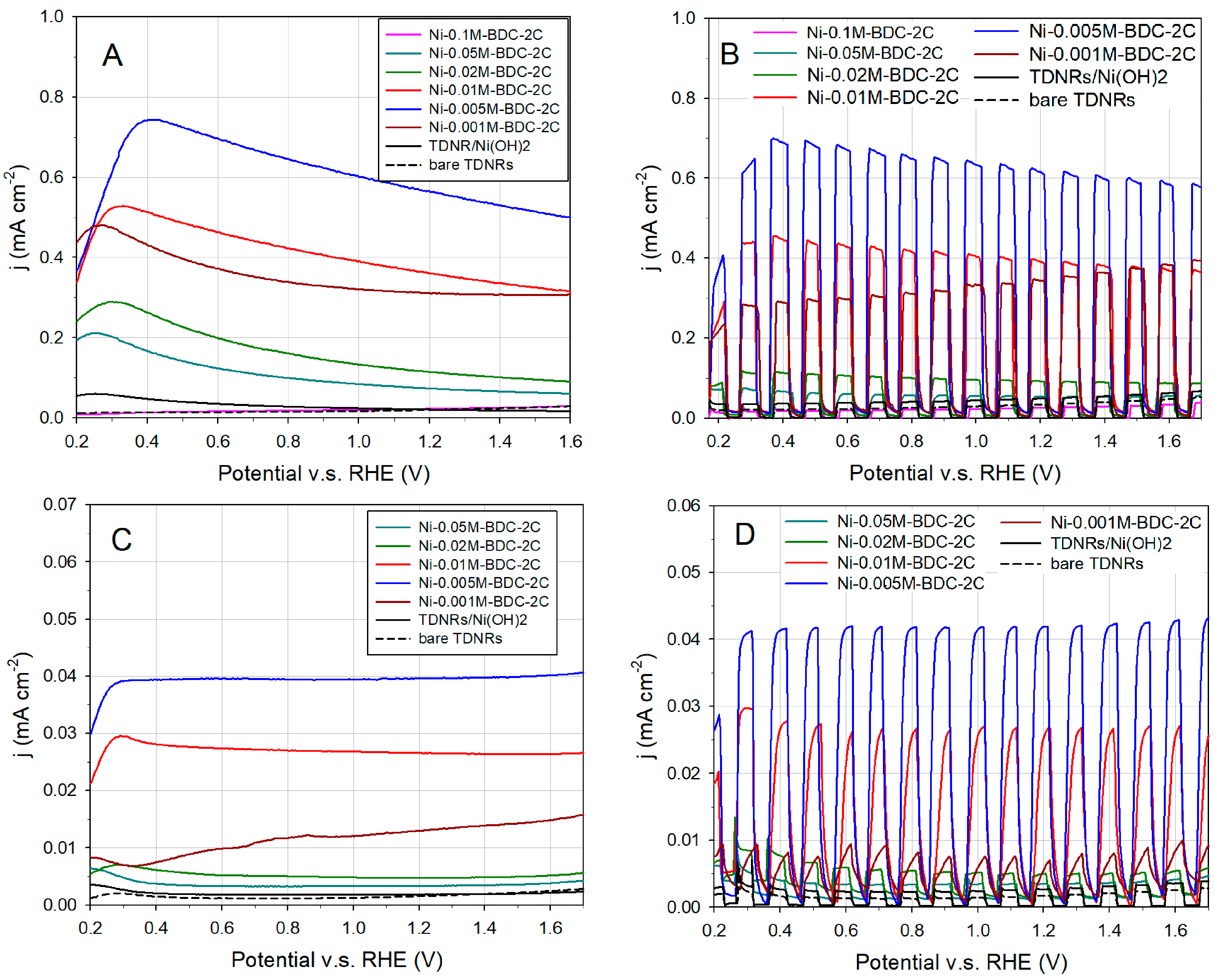
The key properties of any candidate material for application as photocatalyst in photoelectrochemical cell are the photo-response (the ability to absorb visible light, to form and separate electron-hole pairs, and to avoid parasite recombination effects), the electronic conductivity and charge transfer properties (that dictate the charge transfer kinetics), and the long-term chemical stability in contact with the electrolyte. The OER photo-activity of the different Ni-MOF/TDNRs samples, containing different MOF amounts (this was adjusted by controlling the concentration of the nickel coating solution and the number of cycles used for the electrodeposition of Ni hydroxide), are illustrated in Figure 8. The two references cases are bare TiO2 and Ni(OH)2-coated TiO2. Linear sweep voltammograms (LSVs) were recorded under continuous or chopped illumination conditions, using either a UV–Vis or a Vis-only light source, as discussed in the experimental section. A light power density of 100 mW/cm2 was used to facilitate performance comparisons. Under UV–vis irradiation (350–2400 nm wavelengths), a maximum photocurrent density of approximately 0.7 mA/cm2 was obtained with the 0.005M-2C-Ni-MOF/TDNRs sample (blue line, Figure 8A,B). A fast photocurrent change is observed under chopped illumination when the light source is alternatively turned on and off. The peak current density of 0.75 mA/cm2 observed at the potential of 0.4 V/RHE (Figure 8A) is attributed to the oxidation of nickel at the surface of the photoelectrodes.
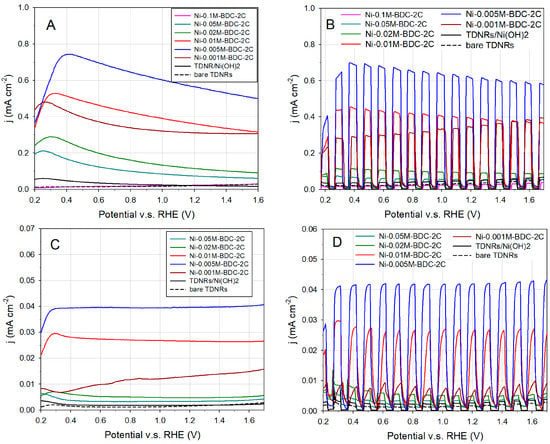
Figure 8.
Linear sweep voltammograms (LSV) measured on the TDNRs photoelectrodes with different concentrations of nickel MOF: (A) LSV curve under UV–Vis light, (B) LSV curve under chopped UV–Vis light (C) LSV curve under visible light, and (D) LSV curve under chopped visible light.
The experiments under visible light irradiation (wavelengths > 420 nm) were performed using a light power density of only 63 mW/cm2. Compared to the experiment performed under UV–Vis light irradiation, the maximum photocurrent density measured on the same 0.005 M-2C-Ni-MOF/TDNRs sample is approximately 15 times less (~40 µA/cm2), as shown in Figure 8C,D. In all experiments, the photocurrent is inversely proportional to the concentration from 0.005 to 0.5 M of Ni-MOF coated onto the electrode. There is almost no photocurrent when either bare TDNRs are used (without the addition of Ni-MOF) or when the TDNRs are coated by the nickel hydroxide only. For comparison, the mean photocurrent measured with the 0.005 M-2C-Ni-MOF/TDNRs sample under visible light irradiation is of 40 µA cm−2, whereas the photocurrent measured on bare TDNRs is only ≈1.0 µA cm−2 and the one measured on Ni(OH)2-coated TiO2 is only ≈2.3 µA cm−2. It is thus clearly evidenced that Ni-MOF nanoparticles act as TiO2 sensitizers. When the nickel hydroxide precursor is used as photosensitizer, a small photocurrent, slightly above the one observed with bare TDNRs, is measured. This lack of OER photoactivity was attributed to its poor electronic conductivity and poor electrocatalytic activity. In addition, the chemical stability of the hydroxide was found to be very low, especially under prolonged polarisation at elevated OER potentials. This hydroxide was used only as a precursor to form the MOF and no attempt was made to optimize its photoactivity and its stability. Improved performances could perhaps be obtained by transformation of the nickel MOF into nickel oxide but this has not been investigated yet because the formation of NiO requires specific experimental conditions and optimization and this is beyond the scope of this paper.
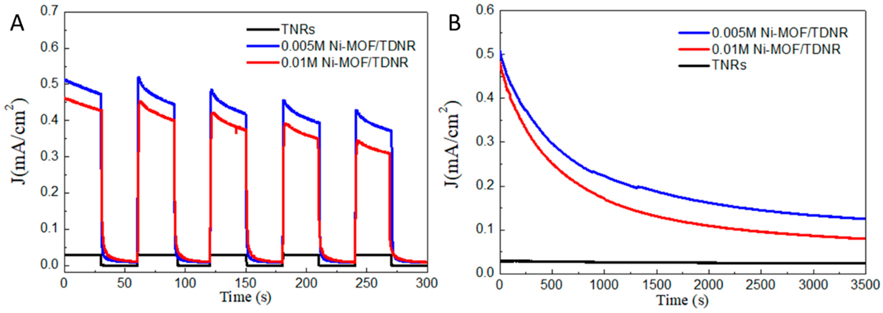
Chronoamperometry experiments have been performed to evaluate the stability of the OER photocurrents. Figure 9A shows the results measured at a working potential of 1 V vs. Ag/AgCl electrode under chopped UV–Vis light irradiation. Three samples are compared: 0.01 M-2C-Ni-MOF/TDNRs, 0.005 M-2C-Ni-MOF/TDNRs (the two MOF-containing samples showing the largest photo-responses) and bare TDNRs for comparison. A decrease in photocurrent was observed in all experiments. The stability was found to depend on the thickness of the co-catalyst MOF layer at the surface. After about an hour of polarization, a plateau is reached with a photocurrent about three times less than the initial value. (Figure 9B). TEM analysis performed after chrono-amperometric ageing tests revealed that the reason for such decrease is not due to a loss of MOF by corrosion/dissolution but possibly to a loss of roughness (reduction in active surface area). Another effect (this was supported by XPS analysis) is the chemical modification of the surface of the MOF layer in contact with the electrolyte where oxygen evolves; the formation of nickel oxide or nickel oxide hydroxide under oxygen evolution is speculated. Annealing the MOF layer could facilitate crystallization and lead to more stable performance. However, ageing and degradation phenomena were not studied in a systematic way and these interpretations and hypotheses need confirmation.
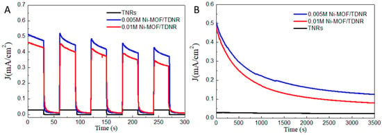
Figure 9.
Chrono-amperometric measurements made on (blue) 0.005M-2C-Ni-MOF/TDNRs, (red) 0.01M-2C-Ni-MOF/TDNRs, and (black) bare TDNRs, under chopped (A) and continuous (B) UV–Vis light irradiation.
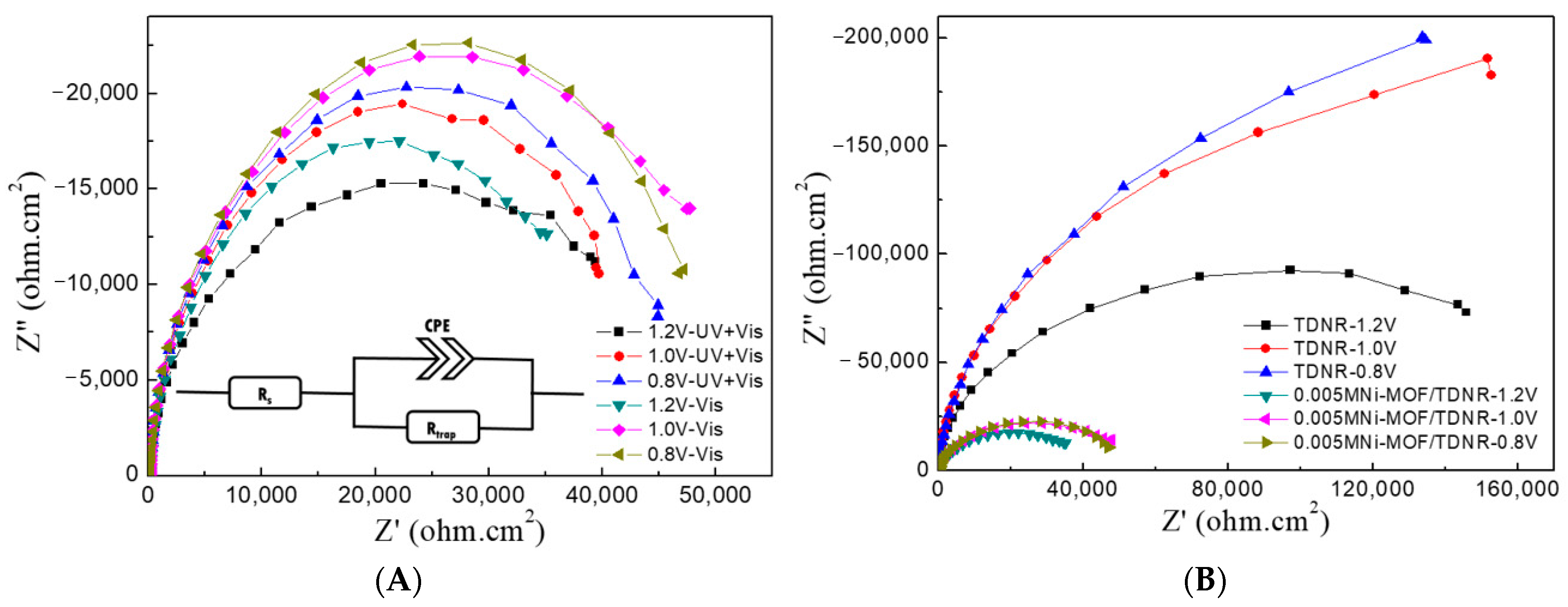
Photo-electrochemical impedance spectroscopy (PEIS) was used in order to analyze the OER mechanism on such systems. PEIS spectra were recorded at different working potentials (0.8 V, 1.0 V, and 1.2 V vs. Ag/AgCl) under UV–vis and visible-only light illumination conditions, using the 0.005M-2C-Ni-MOF/TDNRs, 0.01M-2C-Ni-MOF/TDNRs and bare-TDNRs samples. Typical experimental spectra recorded under UV–Vis or Vis-only light irradiation conditions are shown in Figure 10A,B, respectively. They all contain only one semi-circle along the real axis. Experimental PEIS spectra were fitted using the simple Randles–Ershler model (the equivalent electrical circuit is shown in the inset of Figure 10A) [55], which is commonly used for this type of analysis. In this equivalent circuit, Rs is the electrolyte resistance, the CPE is a constant phase element used to account for the capacitance of the rough photoelectrode/electrolyte interfaces, and Rct is the charge transfer resistance that characterizes the kinetics of electron transfer between water molecules in the electrolyte phase and holes located on surface states. A comparison of the PEIS spectra measured at 1.2 V/RHE on bare TDNRs and on 0.005M-2C-Ni-MOF/TDNRs is provided in Figure S5 (Supporting Information). The values of Rct were determined to be 39.94, and 186.61 kΩ·cm2, respectively (all fit parameters are tabulated in Table S1). The sensitization of the TiO2 nanorods by this nickel MOF led to a reduction in the charge transfer resistance by a factor of 4.7, all other things being equivalent. This is a strong improvement in the level of performance, which demonstrates the role and the photoelectrochemical activity of this MOF with regard to the PEC oxidation of water.
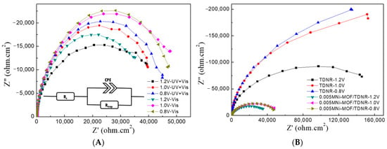
Figure 10.
Photo-electrochemical impedance spectroscopy diagrams measured under UV–vis (A) and Visible (B) light irradiation on 0.005M-2C-Ni-MOF/TDNRs, 0.01M-2C-Ni-MOF/TDNRs and bare-TDNRs.
4. Conclusions
Nanostructured photoelectrodes made of micrometer thin mats of TiO2 nanorod surface sensitized by Ni-MOF nanocoatings have been synthesized using a two-step method consisting of (i) Ni-hydroxide electrodeposition followed by (ii) the solvothermal transformation of the hydroxide into Ni-MOF. The process and the operating conditions have been optimized so that the nanoparticles of Ni-BDC MOF completely and homogeneously cover the TiO2 nanorods. Active layers, approximately 20 nm~50 nm thick, were deposited on the surface of the TiO2 nanorod mats. The photoelectrodes thus prepared exhibit enhanced PEC performance levels and improved charge transfer compared to bare TiO2 nanorods or to TiO2/Ni(OH)2 samples. This was attributed to the successful combination of nickel MOF and TiO2. This combination promotes the oxygen evolution reaction in the PEC cell, and the photosensitizing and photocatalytic roles of nickel MOF have been demonstrated. The obtained nanostructures satisfy the most stringent criteria required for enhancing PEC water-splitting performances: an enlargement of the light absorption range, an improved separation and transfer of photo-excited electron–hole pairs, and an increased surface area resulting from the specific nanostructures obtained. Photoelectrodes prepared from dilute 0.005 M nickel solution yielded the highest photocurrent densities (≈0.7 mA cm−2 were measured under 100 mW/cm2 of UV + visible and 42.4 µA cm−2 under 63 mW/cm2 of luminous intensity of wavelength > 420 nm) compared to nanorods of bare rutile TiO2. By increasing the amount of Ni-MOF in the active layers, the photocurrent density values decreased. This is linked to the appearance of an increasing resistance between Ni-MOF and TDNRs, leading to a decrease in the charge transfer kinetics. The highest level of PEC performance has been achieved by using the thinner layer of Ni-MOF, which improves visible light absorption, produces a high surface area interface, and which leads to efficient charge separation and high mobility of charge carriers. This type of nanostructured active layer (Ni-MOF/TDNR) makes it possible to manufacture efficient photoelectrodes for the photooxidation of water into molecular oxygen. In terms of perspectives, we are trying to further increase the PEC performance of these photoelectrodes by using this MOF of Ni-BDA as a precursor template for the formation of porous nickel oxide nanoparticles, by calcination of Ni-MOF/TDNR samples in oxygen-depleted atmospheres.
Supplementary Materials
The following are available online at https://www.mdpi.com/2673-4141/2/1/4/s1. Figure S1: Experimental EDX spectra of the photoelectrodes prepared by using 0.005M and 0.01M Ni solution and various deposition cycles 2C, 5C, 10C. Figure S2: XRD pattern of different concentration of Ni-MOF on TDNR. Figure S3: XPS spectra of Ni (OH)2/TDNR with zooms on element contributions. Figure S4: XPS Ni 2p spectrum of Ni (OH)2/TDNW and Ni-MOF/TDNW. Figure S5: Experimental (symbols) and calculated (solid lines) PEIS diagrams measured at 1.2V/SCE under visible light illumination on bare TDNRs (■ and 0.005M Ni-MOF/TDNR (●) photoelectrodes. Table S1: Fit parameters of the experimental PEIS spectra of Figure S6 (bare TDNR and 0.005M Ni-MOF/TDNR under visible illumination).
Author Contributions
Conceptualization, All authors; methodology, W.M.A.E.R.; validation, W.M.A.E.R., L.A., P.M. and R.-A.D.; formal analysis, All authors; investigation, S.-M.Y.; resources, P.M. and R.-A.D.; writing—original draft preparation, All authors; writing—review and editing, P.M., R.-A.D. All authors have read and agreed to the published version of the manuscript.
Funding
This research received no external funding.
Data Availability Statement
The data presented in this study are available on request from the corresponding author.
Acknowledgments
The authors wish to thank the Ministry of Education, Taiwan (MOE), for generous financial support under grant no. 1050000778E and the support of the Ministry of Science and Technology (MOST) in Taiwan. The technical support from the characterization platform at ICMMO in Paris-Saclay University, France, is also gratefully acknowledged.
Conflicts of Interest
The authors declare no conflict of interest.
References
- Crabtree, G.W.; Dresselhaus, M.S.; Buchanan, M.V. The Hydrogen Economy. Phys. Today 2004, 57, 39–44. [Google Scholar] [CrossRef]
- GadelHak, Y.; El Rouby, W.M.; Farghali, A.A. Au-decorated 3D/1D titanium dioxide flower-like/rod bilayers for photoelectrochemical water oxidation. Electrochim. Acta 2019, 306, 185–197. [Google Scholar] [CrossRef]
- Becquerel, A.E. Recherches sur les effets de la radiation chimique de la lumiere solaire au moyen des courants electriques. Comptes Rendus L’acad. Des. Sci. 1839, 9, 1. [Google Scholar]
- Fujishima, A.; Honda, K. Electrochemical Photolysis of Water at a Semiconductor Electrode. Nature 1972, 238, 37–38. [Google Scholar] [CrossRef]
- Lyu, F.; Wang, Q.; Choi, S.M.; Yin, Y. Noble-Metal-Free Electrocatalysts for Oxygen Evolution. Small 2019, 15, e1804201. [Google Scholar] [CrossRef]
- Zou, X.; Zhang, Y. Noble metal-free hydrogen evolution catalysts for water splitting. Chem. Soc. Rev. 2015, 44, 5148–5180. [Google Scholar] [CrossRef]
- Mohan, S.; Mao, Y. Dependence of (Photo)electrochemical Properties on Geometry Factors of Hydrothermally Synthesized Delafossite Copper Gallium Oxide CuGaO2toward Oxygen Evolution Reaction. J. Electrochem. Soc. 2018, 165, H607–H613. [Google Scholar] [CrossRef]
- El Rouby, W.M.; Farghali, A.A. Titania morphologies modified gold nanoparticles for highly catalytic photoelectrochemical water splitting. J. Photochem. Photobiol. A Chem. 2018, 364, 740–749. [Google Scholar] [CrossRef]
- Kegel, J.; Povey, I.M.; Pemble, M.E. Zinc oxide for solar water splitting: A brief review of the material’s challenges and associated opportunities. Nano Energy 2018, 54, 409–428. [Google Scholar] [CrossRef]
- Hassan, M.A.; Johar, M.A.; Yu, S.Y.; Ryu, S.-W. Facile Synthesis of Well-Aligned ZnO Nanowires on Various Substrates by MOCVD for Enhanced Photoelectrochemical Water-Splitting Performance. ACS Sustain. Chem. Eng. 2018, 6, 16047–16054. [Google Scholar] [CrossRef]
- Zhang, Z.; Wang, P. Highly stable copper oxide composite as an effective photocathode for water splitting via a facile electrochemical synthesis strategy. J. Mater. Chem. 2012, 22, 2456–2464. [Google Scholar] [CrossRef]
- Paracchino, A.; Mathews, N.; Hisatomi, T.; Stefik, M.; Tilley, S.D.; Grätzel, M. Ultrathin films on copper(i) oxide water splitting photocathodes: A study on performance and stability. Energy Environ. Sci. 2012, 5, 8673–8681. [Google Scholar] [CrossRef]
- Fiorenza, R.; Bellardita, M.; D’Urso, L.; Compagnini, G.; Palmisano, L.; Scirè, S. Au/TiO2-CeO2 Catalysts for Photocatalytic Water Splitting and VOCs Oxidation Reactions. Catalysts 2016, 6, 121. [Google Scholar] [CrossRef]
- You, D.; Pan, B.; Jiang, F.; Zhou, Y.; Su, W. CdS nanoparticles/CeO2 nanorods composite with high-efficiency visible-light-driven photocatalytic activity. Appl. Surf. Sci. 2016, 363, 154–160. [Google Scholar] [CrossRef]
- Malathi, A.; Madhavan, J.; Ashokkumar, M.; Arunachalam, P. A review on BiVO 4 photocatalyst: Activity enhancement methods for solar photocatalytic applications. Appl. Catal. A Gen. 2018, 555, 47–74. [Google Scholar]
- Zhang, J.; Liu, Z.; Liu, Z. Novel WO3/Sb2S3 Heterojunction Photocatalyst Based on WO3 of Different Morphologies for Enhanced Efficiency in Photoelectrochemical Water Splitting. ACS Appl. Mater. Interfaces 2016, 8, 9684–9691. [Google Scholar] [CrossRef]
- Radzi, A.A.S.M.; Safaei, J.; Teridi, M.A.M. Photoelectrochemical enhancement from deposition of BiVO4 photosensitizer on different thickness layer TiO2 photoanode for water splitting application. Nano-Struct. Nano-Objects 2019, 18, 100274. [Google Scholar] [CrossRef]
- Jeong, K.; Deshmukh, P.R.; Park, J.; Sohn, Y.; Shin, W.G. ZnO-TiO2 Core–Shell Nanowires: A Sustainable Photoanode for Enhanced Photoelectrochemical Water Splitting. ACS Sustain. Chem. Eng. 2018, 6, 6518–6526. [Google Scholar] [CrossRef]
- Silipas, T.D.; Indrea, E.; Dreve, S.; Suciu, R.-C.; Rosu, M.C.; Danciu, V.; Cosoveanu, V.; Popescu, V. TiO2—Based systems for photoelectrochemical generation of solar hydrogen. J. Phys. Conf. Ser. 2009, 182, 012055. [Google Scholar] [CrossRef]
- Shen, S.; Chen, J.; Wang, M.; Sheng, X.; Chen, X.; Feng, X.; Mao, S.S. Titanium dioxide nanostructures for photoelectrochemical applications. Prog. Mater. Sci. 2018, 98, 299–385. [Google Scholar] [CrossRef]
- Bae, D.; Seger, B.; Hansen, O.; Vesborg, P.C.; Chorkendorff, I. Durability testing of photoelectrochemical hydrogen production under day/night light cycled conditions. ChemElectroChem 2019, 6, 106–109. [Google Scholar] [CrossRef]
- Bae, D.; Seger, B.; Vesborg, P.C.; Hansen, O.; Chorkendorff, I. Strategies for stable water splitting via protected photoelectrodes. Chem. Soc. Rev. 2017, 46, 1933–1954. [Google Scholar] [CrossRef] [PubMed]
- Antuch, M.; El Rouby, W.; Millet, P. A comparison of water photo-oxidation and photo-reduction using photoelectrodes surface-modified by deposition of co-catalysts: Insights from photo-electrochemical impedance spectroscopy. Int. J. Hydrog. Energy 2019, 44, 9970–9977. [Google Scholar] [CrossRef]
- Carne-Sanchez, A.; Imaz, I.; Stylianou, K.C.; Maspoch, D. Metal-organic frameworks: From molecules/metal ions to crystals to superstructures. Chemistry 2014, 20, 5192–5201. [Google Scholar] [CrossRef]
- Zhang, W.; Wu, Z.Y.; Jiang, H.L.; Yu, S.H. Nanowire-directed templating synthesis of metal-organic framework nanofibers and their derived porous doped carbon nanofibers for enhanced electrocatalysis. J. Am. Chem. Soc. 2014, 136, 14385–14388. [Google Scholar] [CrossRef] [PubMed]
- Ma, T.Y.; Dai, S.; Jaroniec, M.; Qiao, S.Z. Metal-organic framework derived hybrid Co3O4-carbon porous nanowire arrays as reversible oxygen evolution electrodes. J. Am. Chem. Soc. 2014, 136, 13925–13931. [Google Scholar] [CrossRef]
- Li, Z.; Shao, M.; Zhou, L.; Zhang, R.; Zhang, C.; Wei, M.; Evans, D.G.; Duan, X. Directed Growth of Metal-Organic Frameworks and Their Derived Carbon-Based Network for Efficient Electrocatalytic Oxygen Reduction. Adv. Mater. 2016, 28, 2337–2344. [Google Scholar] [CrossRef]
- Wang, Y.; Li, L.; Liang, H.; Xing, Y.; Yan, L.; Dai, P.; Gu, X.; Zhao, G.; Zhao, X. Superstructure of a Metal-Organic Framework Derived from Microdroplet Flow Reaction: An Intermediate State of Crystallization by Particle Attachment. ACS Nano 2019, 13, 2901–2912. [Google Scholar] [CrossRef]
- Jiao, L.; Seow, J.Y.R.; Skinner, W.S.; Wang, Z.U.; Jiang, H.-L. Metal–organic frameworks: Structures and functional applications. Mater. Today 2019, 27, 43–68. [Google Scholar] [CrossRef]
- Gao, X.; Cui, R.; Ji, G.; Liu, Z. Size and surface controllable metal–organic frameworks (MOFs) for fluorescence imaging and cancer therapy. Nanoscale 2018, 10, 6205–6211. [Google Scholar] [CrossRef]
- Chen, J.; Liu, J.; Xie, J.-Q.; Ye, H.; Fu, X.-Z.; Sun, R.; Wong, C.-P. Co-Fe-P nanotubes electrocatalysts derived from metal-organic frameworks for efficient hydrogen evolution reaction under wide pH range. Nano Energy 2019, 56, 225–233. [Google Scholar] [CrossRef]
- Wang, L.; Wu, Y.; Cao, R.; Ren, L.; Chen, M.; Feng, X.; Zhou, J.; Wang, B. Fe/Ni Metal-Organic Frameworks and Their Binder-Free Thin Films for Efficient Oxygen Evolution with Low Overpotential. ACS Appl. Mater. Interfaces 2016, 8, 16736–16743. [Google Scholar] [CrossRef] [PubMed]
- Wang, Q.; Astruc, D. State of the Art and Prospects in Metal–Organic Framework (MOF)-Based and MOF-Derived Nanocatalysis. Chem. Rev. 2019, 120, 1438–1511. [Google Scholar] [CrossRef] [PubMed]
- Bedia, J.; Muelas-Ramos, V.; Peñas-Garzón, M.; Gómez-Avilés, A.; Rodríguez, J.J.; Belver, C. A Review on the Synthesis and Characterization of Metal Organic Frameworks for Photocatalytic Water Purification. Catalysts 2019, 9, 52. [Google Scholar] [CrossRef]
- Chen, Y.-Z.; Zhang, R.; Jiao, L.; Jiang, H.-L. Metal–organic framework-derived porous materials for catalysis. Coord. Chem. Rev. 2018, 362, 1–23. [Google Scholar] [CrossRef]
- Gao, Q.; Xu, J.; Bu, X.-H. Recent advances about metal–organic frameworks in the removal of pollutants from wastewater. Coord. Chem. Rev. 2019, 378, 17–31. [Google Scholar] [CrossRef]
- He, Y.; Chen, F.; Li, B.; Qian, G.; Zhou, W.; Chen, B. Porous metal–organic frameworks for fuel storage. Coord. Chem. Rev. 2018, 373, 167–198. [Google Scholar] [CrossRef]
- Wang, X.; Zhou, J.; Fu, H.; Li, W.; Fan, X.; Xin, G.; Zheng, J.; Li, X. MOF derived catalysts for electrochemical oxygen reduction. J. Mater. Chem. A 2014, 2, 14064–14070. [Google Scholar] [CrossRef]
- Duan, J.; Chen, S.; Zhao, C. Ultrathin metal-organic framework array for efficient electrocatalytic water splitting. Nat. Commun. 2017, 8, 15341. [Google Scholar] [CrossRef]
- Senthil Raja, D.; Lin, H.-W.; Lu, S.-Y. Synergistically well-mixed MOFs grown on nickel foam as highly efficient durable bifunctional electrocatalysts for overall water splitting at high current densities. Nano Energy 2019, 57, 1–13. [Google Scholar] [CrossRef]
- El Rouby, W.M.A.; Antuch, M.; You, S.M.; Beaunier, P.; Millet, P. Novel nano-architectured water splitting photoanodes based on TiO2-nanorod mats surface sensitized by ZIF-67 coatings. Int. J. Hydrog. Energy 2019, 44, 30949–30964. [Google Scholar] [CrossRef]
- El Rouby, W.M.A.; Antuch, M.; You, S.-M.; Millet, P. Surface sensitization of TiO2 nanorod mats by electrodeposition of ZIF-67 for water photo-oxidation. Electrochim. Acta 2020, 339, 135882. [Google Scholar] [CrossRef]
- Zhan, W.W.; Kuang, Q.; Zhou, J.Z.; Kong, X.J.; Xie, Z.X.; Zheng, L.S. Semiconductor@metal-organic framework core-shell heterostructures: A case of ZnO@ZIF-8 nanorods with selective photoelectrochemical response. J. Am. Chem. Soc. 2013, 135, 1926–1933. [Google Scholar] [CrossRef]
- Cai, G.; Zhang, W.; Jiao, L.; Yu, S.-H.; Jiang, H.-L. Template-Directed Growth of Well-Aligned MOF Arrays and Derived Self-Supporting Electrodes for Water Splitting. Chem 2017, 2, 791–802. [Google Scholar] [CrossRef]
- You, S.-M.; El Rouby, W.; Thamilselvan, A.; Tsai, C.-K.; Darmanto, W.; Doong, R.-A.; Millet, P. Fe/Ni Bimetallic Organic Framework Deposited on TiO2 Nanotube Array for Enhancing Higher and Stable Photoelectrochemical Activity of Oxygen Evaluation Reaction. Nanomaterials 2020, 10, 1688. [Google Scholar] [CrossRef]
- Singh, M.K.; Agarwal, A.; Gopal, R.; Swarnkar, R.K.; Kotnala, R.K. Dumbbell shaped nickel nanocrystals synthesized by a laser induced fragmentation method. J. Mater. Chem. 2011, 21, 11074–11079. [Google Scholar] [CrossRef]
- Arrozi, U.S.F.; Bon, V.; Kutzscher, C.; Senkovska, I.; Kaskel, S. Towards highly active and stable nickel-based metal–organic frameworks as ethylene oligomerization catalysts. Dalton Trans. 2019, 48, 3415–3421. [Google Scholar] [CrossRef]
- Gao, C.-Y.; Yang, Y.; Liu, J.; Sun, Z.-M. A NiII-cluster-based MOF as an efficient heterogeneous catalyst for the chemical transformation of CO2. Dalton Trans. 2019, 48, 1246–1250. [Google Scholar] [CrossRef]
- Zhu, D.; Guo, C.; Liu, J.; Wang, L.; Du, Y.; Qiao, S.Z. Two-dimensional metal-organic frameworks with high oxidation states for efficient electrocatalytic urea oxidation. Chem. Commun. 2017, 53, 10906–10909. [Google Scholar] [CrossRef]
- Huang, K.; Xu, Y.; Wang, L.; Wu, D. Heterogeneous catalytic wet peroxide oxidation of simulated phenol wastewater by copper metal–organic frameworks. Rsc. Adv. 2015, 5, 32795–32803. [Google Scholar] [CrossRef]
- Yang, G.; Zhang, Z.; Zhang, S.; Yu, L.; Zhang, P. Synthesis and characterization of highly stable dispersions of copper nanoparticles by a novel one-pot method. Mater. Res. Bull. 2013, 48, 1716–1719. [Google Scholar] [CrossRef]
- Nagamuthu, S.; Ryu, K.-S. Synthesis of Ag/NiO Honeycomb Structured Nanoarrays as the Electrode Material for High Performance Asymmetric Supercapacitor Devices. Sci. Rep. 2019, 9, 4864. [Google Scholar] [CrossRef] [PubMed]
- Santara, B.; Giri, P.K.; Imakita, K.; Fujii, M. Evidence of oxygen vacancy induced room temperature ferromagnetism in solvothermally synthesized undoped TiO2 nanoribbons. Nanoscale 2013, 5, 5476–5488. [Google Scholar] [CrossRef]
- Cheng, X.; Li, Z.; Wu, J. Colossal permittivity in ceramics of TiO2Co-doped with niobium and trivalent cation. J. Mater. Chem. A 2015, 3, 5805–5810. [Google Scholar] [CrossRef]
- Randles, J.E.B. Kinetics of rapid electrode reactions. Discuss. Faraday Soc. 1947, 1, 11–19. [Google Scholar] [CrossRef]
Publisher’s Note: MDPI stays neutral with regard to jurisdictional claims in published maps and institutional affiliations. |
© 2021 by the authors. Licensee MDPI, Basel, Switzerland. This article is an open access article distributed under the terms and conditions of the Creative Commons Attribution (CC BY) license (http://creativecommons.org/licenses/by/4.0/).

