Article

Mole Fraction Dependent Passive Voltage Amplification in FE-DE Heterostructure

by
Archana Chamarahalli Manjunatha
1,
Pratheeksha Suresh
2,
Akshatha Bhat
1,
Vikash Mishra
2,
Yashwanth Nanjappa
1,
Bhaskar Awadhiya
1,* and
Sachin Agrawal
3
1
Department of Electronics and Communication Engineering, Manipal Institute of Technology, Manipal Academy of Higher Education, Manipal 576104, India
2
Department of Physics, Manipal Institute of Technology, Manipal Academy of Higher Education, Manipal 576104, India
3
Department of Electronics and Communication Engineering, National Institute of Technology Delhi, Delhi 110036, India
*
Author to whom correspondence should be addressed.
Electron. Mater. 2025, 6(3), 11; https://doi.org/10.3390/electronicmat6030011
Submission received: 2 March 2025 / Revised: 4 June 2025 / Accepted: 14 July 2025 / Published: 20 August 2025

Abstract

This paper explores ferroelectric–dielectric heterostructures comprising a ferroelectric oxide (Lead Zirconium Titanate ( P b Z r 1 x T i x   O 3 ) ) with a varying mole fraction and a fixed dielectric oxide (Silicon dioxide ( S i O 2 ) ). The study aims to enhance capacitance, optimize voltage amplification, and achieve stable negative capacitance. An isolated ferroelectric capacitor is examined by varying mole fractions of ferroelectric oxide. The negative capacitance in isolated ferroelectric capacitor is highly unstable in nature. The instability problem is fixed and the overall capacitance of the heterostructure is raised while the negative capacitance is stabilized by connecting a dielectric oxide in series with the ferroelectric capacitor. P b Z r 1 x T i x   O 3 is utilized as the ferroelectric oxide, with mole fractions x = 0 , 0.2 , 0.4 , 0.6 , 0.8 , 1.0 . Among the investigated mole fractions, ferroelectric oxide with x = 0.6 offers the maximum voltage amplification and improved capacitance because its capacitance closely matches the dielectric capacitance. Also, dynamic response and temperature analysis of heterostructure are studied further.

1. Introduction

Materials hold immense significance across various industries, with ceramics being widely developed for applications in chemical, electrical, electronic, and mechanical fields. Among these, the perovskite family of ferroelectrics has been extensively researched and is well recognized. These materials are characterized by the general formula A B O 3 , where A and B are cations of varying sizes and O represents an anion [1,2]. Lead zirconate titanate ( P b Z r 1 x T i x O 3 ) , commonly known as P Z T , is particularly notable for its outstanding ferroelectric and piezoelectric properties [3]. This ceramic compound aligns to A B O 3 structure, with Zirconium ( Z r ) and titanium ( Ti ) serving as B -site dopants. The Zr / Ti ratio plays a critical role in modifying the material’s film properties, enabling it to be optimized for various applications [4,5]. With the continuous downscaling of CMOS technology, increased leakage currents and short-channel effects have emerged as critical challenges [6]. One effective approach to lower these issues is by reducing the supply voltage, as dynamic power dissipation is proportional to the square of the supply voltage   ( P d y n V D D 2 ) . However, lowering the supply voltage also reduces the ON current, thereby diminishing transistor speed I o n V D D V T   α [7]. To maintain sufficient ON current and operational speed, the threshold voltage   V T must be reduced. Unfortunately, decreasing the threshold voltage leads to an increase in OFF current I O F F   10 V T S S , which in turn causes an increase in the transistor’s static power dissipation ( P O F F I O F F ) . This conflicting criterion implies that there is always a trade-off between effectiveness and power dissipation [8,9]. Although transistor dimensions continue to shrink with advancements in CMOS technology, reducing the operating voltage remains a challenge due to the inherent 60 mV/decade limit of the subthreshold swing [10]. Ferroelectric material is known for the property of negative capacitance (NC), which can reduce the subthreshold swing below Boltzmann limit [11]. Ferroelectric materials exhibit spontaneous polarization, setting them apart from dielectric materials, where polarization charge maintains a linear relationship with the applied electric field. This unique property allows ferroelectric materials to remain polarized even in the absence of an electric field, and their polarization direction can be reversed by applying an external electric field [12,13]. Ferroelectric oxides offer significant advantages, including reduced subthreshold swing and enhanced amplification in electronic devices. When integrated with conventional MOSFETs, these materials enable subthreshold swings below 60 mV/decade, attributed to their negative capacitance effect and switchable polarization. However, ferroelectric oxide’s negative capacitance state is inherently unstable. By connecting a dielectric oxide in series with the ferroelectric oxide, this can be stabilized [14,15]. Ferroelectric–dielectric (FE-DE) heterostructures are the basic building blocks of NCFET, and their investigation is driven by the special characteristics of ferroelectric oxides [16,17,18,19]. Three crucial facets of ferroelectric–dielectric heterostructures—enhancement of capacitance, voltage amplification, and stabilization of NC—are examined. The schematic and circuit of the FE-DE heterostructure are shown in Figure 1. Although the presence of a resistive component makes the capacitor leaky in nature, we still consider it to be non-leaky because the resistive and capacitive components are independent of each other and the potential at node A depends only on capacitance values and is unaffected by the presence of resistance [20]. In this heterostructure, we have considered Lead Zirconium Titanate ( P b Z r 1 x T i x O 3 ) and S i O 2 as ferroelectric and dielectric material, respectively. P b Z r 1 x T i x O 3 is utilized as the ferroelectric oxide, with mole fractions x = 0 , 0.2 , 0.4 , 0.6 , 0.8 , 1.0 . PZT is highly favoured in ferroelectric applications due to its exceptional properties, such as resilience to variations in film thickness and swift polarization reversal. These features make it an ideal choice for a wide range of MEMS (Micro-Electro-Mechanical Systems) applications [21,22,23].
S i O 2 is chosen for its simplicity in fabrication on silicon substrates, achieved through the straightforward process of oxidizing a silicon wafer [14]. The simulation parameters include dimensions of A = 45   n m × 1   µ m , t D E = 1   n m , t F E = 200   n m . The simulation uses silicon dioxide, which has a permittivity of 3.9. The mathematical equations (general and differential) are solved and plotted using the MATLAB R2024b by using the ezplot command. The initial conditions are set to zero. This study enables the proper selection of mole fraction in lead zirconium titanate when used in FE-DE heterostructures with the dimensions mentioned in the article. Further, the study can be useful in the design of Negative Capacitance Field Effect transistors [24,25]. Ferroelectric thickness for lead zirconium titanate is selected as 200 nm because it guarantees adequate polarisation switching to sustain negative capacitance. Thicker ferroelectric thickness may result in hysteresis in device characteristics. The thin dielectric layer (1 nm) ensures the capacitance matching between ferroelectric and dielectric capacitance, hence maximizing the voltage drop across the ferroelectric, thereby enhancing voltage amplification across the dielectric.

2. Isolated Ferroelectric Capacitor

The Landau–Khalatnikov equation establishes a correlation involving charge and voltage across a FE capacitor provided the source of voltage is coupled to an isolated ferroelectric material.
  V F = α Q F + β Q F 3 + γ Q F 5 + ρ d Q F d t  
where Q F and V F stand for the ferroelectric capacitor’s charge and voltage, respectively. For the ferroelectric material, the anisotropy constants α , β , and γ are defined as follows:
T o = 462.63 + 843.4 x 2105.5 x 2 + 4041.8 x 3 3828.3 x 4 + 1337.8 x 5
C o = 2.1716 1 + 500.05 ( x 0.5 ) 2 + 0.131 x + 2.01 × 10 5 ; w h e n   0 x 0.5
C o = 2.8339 1 + 126.56 ( x 0.5 ) 2 + 1.4132 × 10 5 ; w h e n   0.5 x 1.0
α = T T o 2 ϵ o C o  
β = ( 10.612 22.655 x + 10.955 x 2 ) × 10 13 } / C o  
γ = ( 12.026 17.296 x + 9.179 x 2 ) × 10 13 } / C o  
where T is the absolute temperature, T o is the Curie–Weiss temperature, C o is the Curie Constant, and ϵ o is the permittivity of free space.
Equation (1) can be expressed under steady-state conditions as
V F = α Q F + β Q F 3 + γ Q F 5  
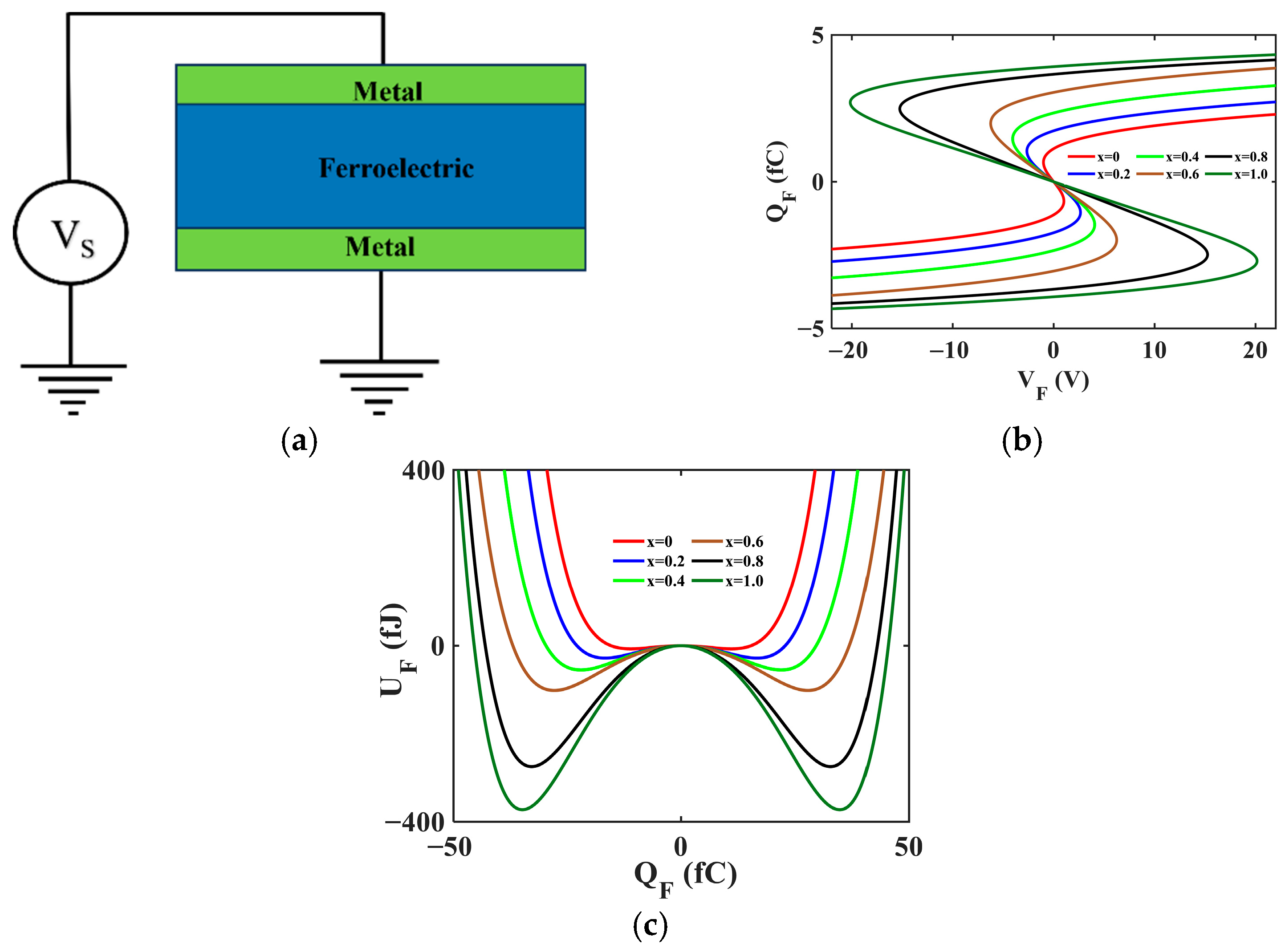
The solution to Equation (5) is displayed in Figure 2b, which yields the S-shaped relationship between charge and voltage that isolated FE material exhibits for a range of mole fractions. The charge decreases as the voltage increases, which confirms negative capacitance in isolated ferroelectric material. In comparison to other mole fractions, the ferroelectric material with a mole fraction of x = 1.0 exhibits a larger coercive voltage, indicating that the negative capacitance state lasts longer for x = 1.0 . The expression for a ferroelectric material’s free energy U F is
U F = α 2 Q F 2 + β 4 Q F 4 + γ 6 Q F 6  
The energy topography of an isolated ferroelectric capacitor, depicted in Figure 2c, reveals that for every value of the mole fraction, the parabolic curve is inverted. This inversion confirms the existence of negative capacitance. The NC state is inherently unstable, which can be understood by considering a charge placed at the crest of the parabola. Such a charge would naturally move toward one of the minima, illustrating the instability of the isolated FE material. The values of the anisotropy constants are given in Table 1. It is interesting to note that the anisotropy constant ( β ) has a negative value for x = 0.8 and 1 , which means the PZT is behaving as the first-order transition material. β has a positive value for other values of mole fraction and PZT behaves as a second-order transition material. Due to the negative value of the capacitance value for the mole fraction, 0.8 and 1 are lower but the magnitude is higher, which is discussed in the upcoming section and is responsible for hysteresis. A ferroelectric capacitor’s negative capacitance scenario can be stabilized by connecting a dielectric capacitor in series with it. The following section discusses the simulation findings for the heterostructure.

3. Ferroelectric Capacitor Connected in Series with Dielectric Capacitor

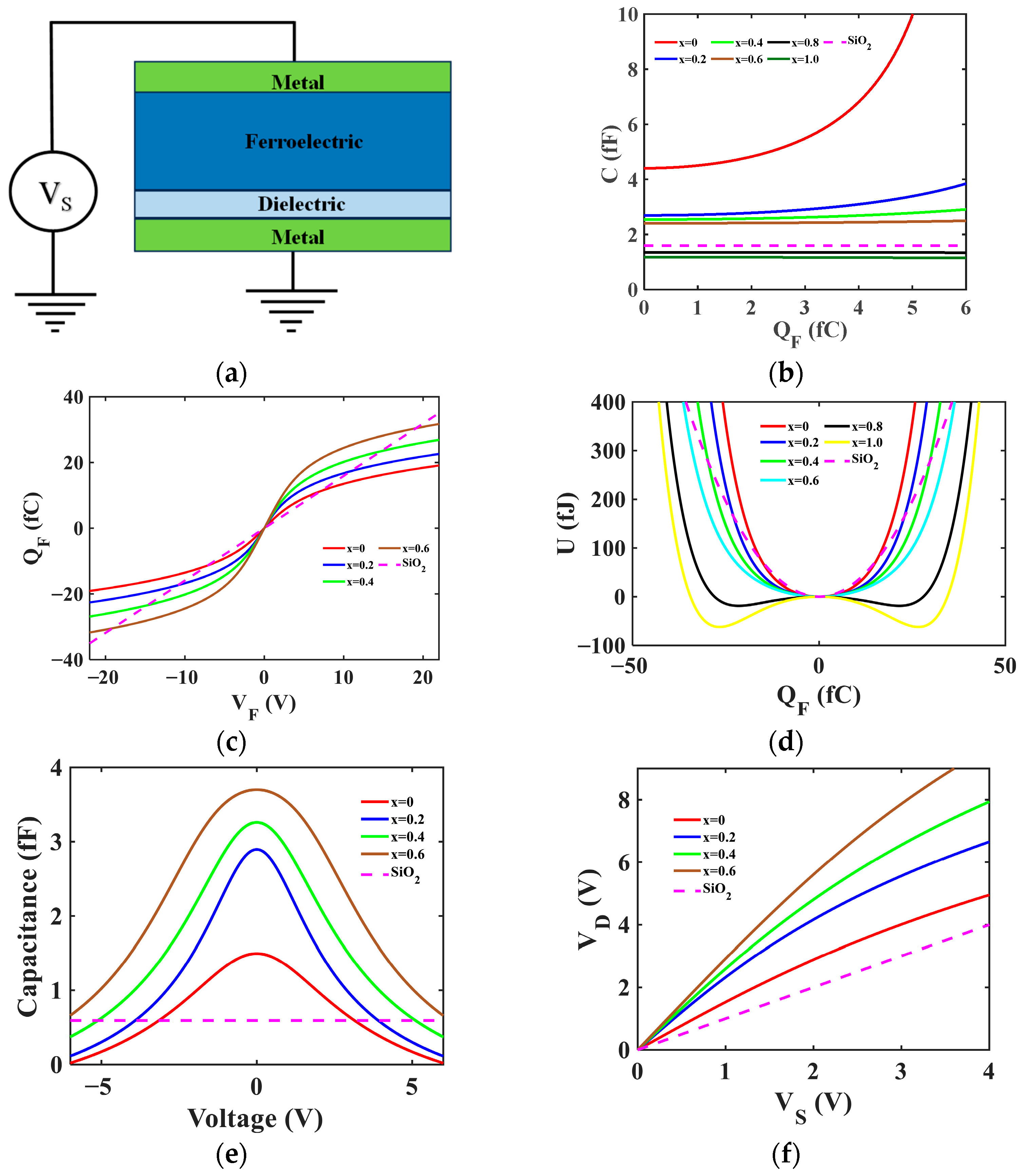
Figure 3a illustrates the schematic diagram of an FE-DE heterostructure. The unstable negative capacitance of an isolated ferroelectric material is stabilized by incorporating a dielectric capacitor in series, provided that the dielectric capacitance satisfies the condition ( C D < 1 / α ) where α is the anisotropy constant. Notably, when the ferroelectric capacitance is comparable to the dielectric capacitance, significant voltage amplification is observed. Figure 3b presents the capacitance versus charge characteristics. For a ferroelectric material with a mole fraction of 0.6, the ferroelectric capacitance closely matches the dielectric capacitance ( C F E C D E ) , making it the most favorable for achieving optimal performance.
In contrast, ferroelectric materials with mole fractions of 0.8 and 1.0 exhibit capacitance values lower than the dielectric capacitance ( C F E < C D E ) , and therefore for these values of mole fractions the heterostructure would be showing hysteresis and hence is excluded from further analysis. Since the dielectric and ferroelectric capacitors are connected in series, they store the same amount of charge. By applying Kirchhoff’s Voltage Law (KVL) to the heterostructure, the voltage distribution across the components can be analyzed.
  V S = V F + V D  
  V F = ρ   d Q F d t + α Q F + β Q F 3 + γ Q F 5  
  V D = Q D C D = Q F C D  
  V S = ρ   d Q F d t + α + 1 C D   Q F + β Q F 3 + γ Q F 5  
Figure 3c illustrates the charge versus voltage characteristics of the ferroelectric–dielectric heterostructure in a steady state for different mole fractions of the ferroelectric material. Mole fractions of 0, 0.2, 0.4, and 0.6 display no indications of negative capacitance, confirming the presence of positive capacitance and stable behaviour.
Additionally, the overall energy stored in the FE-DE heterostructure is the sum of the individual energies stored in the ferroelectric and dielectric capacitors.
U = U F + U D  
The energy topography of the heterostructure for FE material with varying mole fractions is depicted in Figure 3d. From the graph, it is evident that with the combination of FE and DE capacitors in series the overall system energy is minimized, leading to the stabilization of the negative capacitance. Likewise, the twin-well in the energy topography will advent adjacent to each other and the curve becomes flatter. The observed flattening of the energy landscape indicates a correlation with an increase in the capacitance of the heterostructure. Capacitance can be expressed in terms of energy using the formula
1 C =   d 2 U d Q 2  
The energy landscape shows the greatest flatness at a mole fraction of x = 0.6 , indicating significant capacitance enhancement in the heterostructure at this composition. In a series combination of positive capacitors, the overall capacitance is generally smaller than the capacitance of any individual capacitor in the series. The observed increase in capacitance, however, seems to defy the fundamental principles of circuit theory and electrostatics. This apparent contradiction can only be explained by the presence of negative capacitance. The formula for calculating the overall capacitance in a series combination is expressed as
1 C = 1 C F + 1 C D  
Here, C can be greater than C D , if C F is negative and |   C F   | > C D . The capacitance vs. voltage of the ferroelectric–dielectric heterostructure for various FE mole fractions is displayed in Figure 3e. The representation illustrates enhancement of capacitance since the equivalence of the FE and DE capacitances is higher than the DE capacitance, which is only achievable when one of the capacitances is negative. The graph shows that, in comparison to other mole fractions, capacitance has increased for mole fraction x = 0.6 . It is possible to express the relationship between supply voltage, ferroelectric capacitor, and voltage across dielectric capacitor as follows:
  V D = V S V F  
  V D = V S × 1 V F V S    
The mathematical relation among supply voltage and voltage dropped across dielectric can be represented by the equation
V D = V S × C F C F + C D  
V D = V S × | C F | C F C D  
Equation (17) states that when | C F   | > C D , V D can be higher than V S , meaning that a slight change in V S can have a significant impact on V D . The results support passive voltage amplification in the FE–DE heterostructure, as they show that the voltage across the dielectric is greater than the applied voltage. The voltage across the DE is plotted against the supply voltage in Figure 3f. It is evident from Figure 3f that when the voltage across the dielectric ( V D ) is plotted against the supply voltage ( V S ) , a greater degree of voltage amplification is shown for the FE material with a mole fraction of x = 0.6 . Figure 4a shows the plot of the differential voltage amplification ( d V D d V S ) in the ferroelectric–dielectric heterostructure with respect to V S . It shows how the heterostructure’s voltage amplification varies with the supply voltage. Comparing ferroelectric material with different mole fractions, the one with x = 0.6 offers the greatest differential voltage amplification.

4. Dynamic Response of Heterostructure

  V S = α Q F + β Q F 3 + γ Q F 5 + ρ d Q F d t + Q F C D  
Figure 4b depicts the charge variation over time when a triangular pulse of 1 V with a frequency of 100 MHz is applied to the heterostructure’s input. The charge versus time graph for ferroelectric materials in FE-DE heterostructures shows that as the mole fraction of FE increases from 0 to 0.6, the stored charge gradually increases, reaching its maximum at x = 0.6 . Among the tested compositions, ferroelectric material with x = 0.6 exhibits the highest charge compared to other values of x . Substituting Q F = Q D = V D   C D into the preceding equation leads to Equation (19).
  V S = α V D C D + β V D 3 C D 3 + γ V D 5 C D 5 + ρ d V D C D d t + V D C D C D  
According to Equation (19), voltage is proportional to capacitance ( C D ) . Since capacitance is highest at x = 0.6 , voltage amplification is also maximized at this point. Figure 4c depicts the variation in the voltage drop across the dielectric over time. For x = 0.6 , the voltage amplification over time is the highest compared to other mole fractions.

5. Temperature Analysis of Heterostructure

This section presents a temperature analysis of the heterostructure. Notably, an increase in temperature in an isolated ferroelectric capacitor exhibits a similar effect to adding a dielectric capacitor in series with the ferroelectric capacitor. This analogy arises from the temperature dependence of the anisotropy constant ( α ) . At lower charge levels, the capacitance of an isolated ferroelectric capacitor can be estimated using the following equation.
C F E 1 α  
Here, α represents the temperature-dependent anisotropy constant for PZT, expressed as α = α 0   ( T T 0 ) .
C F E = 1 α 0 T T 0  
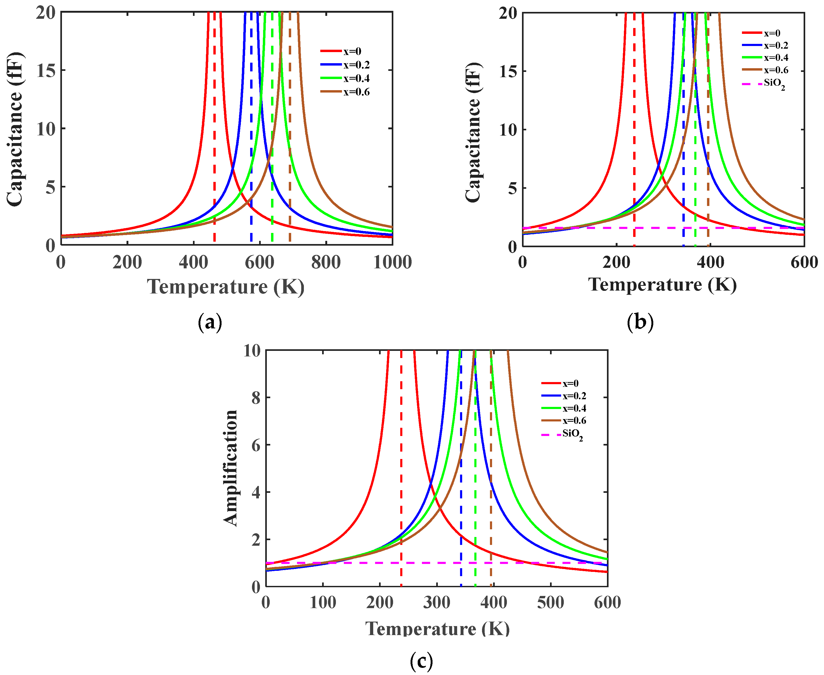
Figure 5a shows the variation of capacitance in an isolated ferroelectric capacitor with temperature. The graph indicates that the capacitance of the ferroelectric increases with temperature up to the Curie temperature. Beyond this point, further increase in temperature causes a decrease in capacitance. This trend is consistent across all compositions. Figure 5b illustrates the capacitance of the ferroelectric–dielectric heterostructure as a function of temperature. When a FE capacitor is added in series with the DE capacitor, the Curie temperature shifts to a lower value for all mole fractions of the ferroelectric material. The new Curie–Weiss temperature is given by T 0 1 ( α 0   C D E ) . Figure 5c highlights the voltage amplification of the ferroelectric–dielectric heterostructure as a function of temperature.
A m p l i f i c a t i o n : V D V S = 1 C D E α 0 T T 0  
Voltage amplification concerning temperature is plotted for the considered ferroelectric material compositions. Voltage amplification is highest when the temperature reaches its new Curie–Weiss temperature, which is because after Curie temperature the ferroelectric material is converted into the dielectric material. This trend is visible for all the values of the mole fraction.

6. Conclusions

The study shows that the FE-DE heterostructure can significantly increase capacitance, boost voltage, and stabilize negative capacitance. The composition with x = 0.6 was found to be best by analyzing various mole fractions of Lead Zirconium Titanate ( P b Z r 1 x   T i x O 3 ) . This composition offers the highest voltage amplification since ferroelectric and dielectric capacitances closely match. Further information about the heterostructure’s operational stability and performance is also provided by its dynamic response and temperature analysis. These characteristics highlight its potential for sophisticated electronic applications, including advanced transistors, high-density memory devices, high-performance capacitors, and energy harvesting systems, where precise control over capacitance and voltage amplification is essential.

Author Contributions

Conceptualization, B.A. and A.C.M.; methodology, B.A., P.S. and A.C.M. software, P.S., A.B. and A.C.M.; validation, P.S., A.B. and A.C.M.; formal analysis, P.S., A.B. and A.C.M.; investigation, P.S., A.B. and A.C.M.; resources, P.S., A.B. and A.C.M.; data curation, P.S., A.B. and A.C.M.; writing—original draft preparation, P.S., A.B., B.A., Y.N. and A.C.M.; writing—review and editing, P.S., A.B., B.A., Y.N. and A.C.M.; visualization, P.S., A.B., B.A., Y.N. and A.C.M.; supervision, V.M., Y.N., B.A. and S.A.; project administration, Y.N. and B.A. All authors have read and agreed to the published version of the manuscript.

Funding

This research received no external funding.

Data Availability Statement

Data is contained within the article.

Conflicts of Interest

The authors declare no conflict of interest.

References

  1. Tiwari, B.; Babu, T.; Choudhary, R.N.P. Review on Different Preparation Techniques of Lead Zirconate Titanate. Int. Res. J. Adv. Sci. Hub 2020, 2, 121–126. [Google Scholar] [CrossRef]
  2. Bowen, C.R.; Kim, H.A.; Weaver, P.M.; Dunn, S. Piezoelectric and ferroelectric materials and structures for energy harvesting applications. Energy Environ. Sci. 2014, 7, 25–44. [Google Scholar] [CrossRef]
  3. Ren, T.L.; Zhao, H.J.; Liu, L.T.; Li, Z.J. Piezoelectric and ferroelectric films for microelectronic applications. Mater. Sci. Eng. B 2003, 99, 159–163. [Google Scholar] [CrossRef]
  4. Sriram, S.; Bhaskaran, M.; Mitchell, A. Piezoelectric Thin Film Deposition: Novel Self-Assembled Island Structures and Low Temperature Processes on Silicon. In Piezoelectric Ceramics; Suaste-Gomez, E., Ed.; Sciyo: Rijeka, Croatia, 2010. [Google Scholar] [CrossRef]
  5. Awadhiya, B.; Kondekar, P.N.; Meshram, A.D. Analogous behavior of FE-DE heterostructure at room temperature and ferroelectric capacitor at Curie temperature. Superlattices Microstruct. 2018, 123, 306–310. [Google Scholar] [CrossRef]
  6. Singh, S.; Gupta, R.; Priyanka; Singh, R.; Bhalla, S.K. Design and Simulation-Based Analysis of Triple Metal Gate with Ferroelectric-SiGe Heterojunction Based Vertical TFET for Performance Enhancement. Silicon 2022, 14, 11015–11025. [Google Scholar] [CrossRef]
  7. Rahi, S.B.; Tayal, S.; Upadhyay, A.K. A review on emerging negative capacitance field effect transistor for low power electronics. Microelectron. J. 2021, 116, 105242. [Google Scholar] [CrossRef]
  8. Kobayashi, M.; Hiramoto, T. On device design for steep-slope negative-capacitance field-effect-transistor operating at sub-0.2V supply voltage with ferroelectric HfO2 thin film. AIP Adv. 2016, 6, 025113. [Google Scholar] [CrossRef]
  9. Ratnesh, R.K.; Goel, A.; Kaushik, G.; Garg, H.; Chandan; Singh, M.; Prasad, B. Advancement and challenges in MOSFET scaling. Mater. Sci. Semicond. Process. 2021, 134, 106002. [Google Scholar] [CrossRef]
  10. Rai, A.; Gupta, D.; Mishra, H.; Nandan, D.; Qamar, S. Beyond Si-Based CMOS Devices: Needs, Opportunities, and Challenges. In Beyond Si-Based CMOS Devices: Materials to Architecture; Singh, S., Sharma, S.K., Nandan, D., Eds.; Springer Nature: Singapore, 2024; pp. 3–25. [Google Scholar] [CrossRef]
  11. Awadhiya, B.; Kondekar, P.N.; Yadav, S.; Upadhyay, P.; Jaisawal, R.K.; Rathore, S. Effect of Scaling on Passive Voltage Amplification in FE-DE Hetero Structure. In Proceedings of the 2021 International Conference on Control, Automation, Power and Signal Processing (CAPS), Jabalpur, India, 10–12 December 2021; pp. 1–4. [Google Scholar] [CrossRef]
  12. Bain, A.K.; Chand, P. Ferroelectrics: Principles and Applications; John Wiley & Sons: Hoboken, NJ, USA, 2017. [Google Scholar]
  13. Haertling, G.H. Ferroelectric Ceramics: History and Technology. J. Am. Ceram. Soc. 1999, 82, 797–818. [Google Scholar] [CrossRef]
  14. Awadhiya, B.; Kondekar, P.N.; Meshram, A.D. Passive voltage amplification in non-leaky ferroelectric–dielectric heterostructure. Micro. Nano Lett. 2018, 13, 1399–1403. [Google Scholar] [CrossRef]
  15. Khan, A.I.; Radhakrishna, U.; Salahuddin, S.; Antoniadis, D. Work Function Engineering for Performance Improvement in Leaky Negative Capacitance FETs. IEEE Electron Device Lett. 2017, 38, 1335–1338. [Google Scholar] [CrossRef]
  16. Jain, A.; Alam, M.A. Stability Constraints Define the Minimum Subthreshold Swing of a Negative Capacitance Field-Effect Transistor. IEEE Trans. Electron Devices 2014, 61, 2235–2242. [Google Scholar] [CrossRef]
  17. Khan, A.I. On the Microscopic Origin of Negative Capacitance in Ferroelectric Materials: A Toy Model. In Proceedings of the 2018 IEEE International Electron Devices Meeting (IEDM), Atlanta, GA, USA, 1–5 December 2018; pp. 9.3.1–9.3.4. [Google Scholar] [CrossRef]
  18. Wong, J.C.; Salahuddin, S. Negative Capacitance Transistors. Proc. IEEE 2019, 107, 49–62. [Google Scholar] [CrossRef]
  19. Liu, T.; Yang, C.; Si, J.; Sun, W.; Su, D.; Li, C.; Yuan, X.; Huang, S.; Cheng, X.; Cheng, Z. Self-Poled Bismuth Ferrite Thin Film Micromachined for Piezoelectric Ultrasound Transducers. Adv. Mater. 2025, 37, 2414711. [Google Scholar] [CrossRef] [PubMed]
  20. Khan, A.I.; Radhakrishna, U.; Chatterjee, K.; Salahuddin, S.; Antoniadis, D.A. Negative Capacitance Behavior in a Leaky Ferroelectric. IEEE Trans. Electron Devices 2016, 63, 4416–4422. [Google Scholar] [CrossRef]
  21. Trolier-McKinstry, S.; Zhu, W.; Akkopru-Akgun, B.; He, F.; Ko, S.W. Reliability of piezoelectric films for MEMS. Jpn. J. Appl. Phys. 2023, 62, SM0802. [Google Scholar] [CrossRef]
  22. Kumar, B.N.; Babu, T.; Tiwari, B.; Choudhary, R.N.P. Review on PZT as a mechanical engineering material. Ferroelectrics 2024, 618, 125–138. [Google Scholar] [CrossRef]
  23. Chugh, D.; Kwon, H.K.; Haddon-Vukasin, G.D.; Kenny, T.W.; Chandorkar, S.A. Sensing Voltage at Electrically Floating Nodes: A Path Toward Enhancing Performance and Robustness in Capacitive MEMS Resonators. J. Microelectromech. Syst. 2025, 34, 116–133. [Google Scholar] [CrossRef]
  24. Lamba, A.; Chaujar, R.; Deen, M.J. Negative capacitance FinFETs for low power applications: A review. Micro. Nanostruct. 2025, 205, 208177. [Google Scholar] [CrossRef]
  25. Kumar, A.; Chaturvedi, S.; Kumar, S. Negative capacitance double-gate MOSFET for advanced low-power electronic applications. Microelectron. J. 2025, 159, 106656. [Google Scholar] [CrossRef]
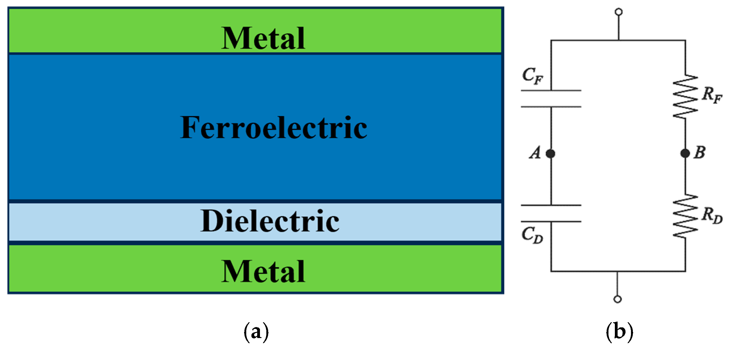
Figure 1. (a) Schematic and (b) circuit configuration of Ferroelectric–Dielectric Heterostructure.
Electronicmat 06 00011 g001
Figure 2. (a) Schematic of an isolated ferroelectric capacitor connected to a voltage source; (b) Q-V characteristics and (c) energy versus charge attributes of the isolated FE capacitor for various mole fractions.
Electronicmat 06 00011 g002
Figure 3. (a) Illustration of the ferroelectric–dielectric capacitor linked to a voltage source {(b) C-Q characteristics; (c) Q-V characteristics; (d) energy versus charge characteristics; (e) capacitance; (f) Voltage Amplification} of FE-DE heterostructure for varying mole fractions.
Electronicmat 06 00011 g003
Figure 4. {(a) ( d V D / d V S ) versus   V S (b) charge versus time (c) voltage versus time} in FE-DE heterostructure.
Electronicmat 06 00011 g004
Figure 5. (a) Capacitance versus temperature characteristics of isolated ferroelectric capacitor {(b) Capacitance versus temperature; (c) Amplification versus temperature} characteristics of FE-DE heterostructure for different mole fractions.
Electronicmat 06 00011 g005
Table 1. Anisotropy Constants for Ferroelectric Oxide.
P b Z r 1 x T i x   O 3 α ( 1 / F ) β ( 1 / F C 2 ) γ ( 1 / F C 4 )
x = 0 2.27 × 10 14 1.64 × 10 42 1.16 × 10 69
x = 0.2 3.71 × 10 14 9.78 × 10 41 8.38 × 10 68
x = 0.4 3.93 × 10 14 4.25 × 10 41 5.30 × 10 68
x = 0.6 4.15 × 10 14 1.12 × 10 41 3.63 × 10 68
x = 0.8 7.38 × 10 14 9.68 × 10 40 4.83 × 10 68
x = 1.0 8.50 × 10 14 2.29 × 10 41 5.09 × 10 68
Disclaimer/Publisher’s Note: The statements, opinions and data contained in all publications are solely those of the individual author(s) and contributor(s) and not of MDPI and/or the editor(s). MDPI and/or the editor(s) disclaim responsibility for any injury to people or property resulting from any ideas, methods, instructions or products referred to in the content.