Article

Tribological, Thermal, Kinetic, and Surface Microtextural Characterization of Prime p-Type <100> Silicon Wafer CMP for Direct Wafer Bonding Applications

1
Araca, Inc., Tucson, AZ 85750, USA
2
Fujimi Corporation, Tualatin, OR 97062, USA
3
Department of Chemistry, Lewis University, Romeoville, IL 60446, USA
*
Author to whom correspondence should be addressed.
Electron. Mater. 2025, 6(1), 1; https://doi.org/10.3390/electronicmat6010001
Submission received: 13 September 2024 / Revised: 29 October 2024 / Accepted: 17 December 2024 / Published: 8 January 2025

Abstract

:
We investigated the tribological, thermal, kinetic, and surface microtextural characteristics of chemical mechanical polishing (CMP) of 300 mm p-type <100> prime silicon wafers (and their native oxide) at various pressures, sliding velocities, and starting platen temperatures. Results showed the dominant tribological mechanism for both native oxide and silicon polishing to be boundary lubrication. Using frictional data, we pinpointed the exact time that corresponded to the total removal of the native oxide and the onset of silicon polishing. This allowed us to separately characterize removal rates of each layer. For native oxide, while the rate depended on temperature, the presence of a temperature-independent shear force threshold and the low observed rates suggested that its removal by the slurry was dominantly mechanical. In contrast, for silicon polish, the absence of a distinctive shear force threshold and the fact that, for the same set of consumables, rates were more than 200 times larger for silicon than for native oxide suggested a dominantly chemical process with an average apparent activation energy of 0.34 eV. It was further confirmed that rate selectivity between native oxide and PE-TEOS based SiO2 control wafers was around 1 to 7, which underscored the importance of being able to directly measure native oxide removal rates. In all cases, we achieved excellent post-polish surfaces with Sa and Sq values of below 1 nm. Due to thermal softening of the thermoplastic pad at elevated temperatures, which we confirmed via dynamic mechanical analysis, overall process vibrations were significantly higher when platen heating was employed.

1. Introduction

Chemical mechanical polishing (CMP) of prime silicon wafers has been mainstream for more than four decades due partly to the resulting high-quality surface finish and reasonable removal rates during the final polishing unit operation [1,2,3,4,5,6,7]. In integrated circuit manufacturing, silicon and polysilicon CMP have also been widely adopted for fabricating metal-oxide-semiconductor field-effect transistors (MOSFETs), backside power delivery (BPD), gate electrodes, NAND flash memory devices, floating gates for fin field-effect transistors (FinFETs), and microelectromechanical system (MEMS) devices, all made possible due to controllable removal rates and excellent surface quality [8,9,10,11,12,13,14]. However, not until recently has the drive for direct wafer bonding brought forth the need for extremely high silicon removal rates (i.e., greater than 1.5 microns per minute) while ensuring a high-quality wafer surface (i.e., relatively defect-free with surface roughness values that are below 1 nm) that is also hydrophilic (i.e., OH-terminated) [15,16,17,18,19,20]. It is important to note that all prime silicon wafers have multiple mono-layers of native oxide on their surfaces [21,22,23,24,25,26,27]. The thickness of the native oxide differs depending on factors such as the final chemical treatment of the silicon wafer, its subsequent storage time, and the environment in which it is stored [21,22,23,24,25,26,27]. Given the fact that silicon polishing slurries have historically had low removal rate selectivities to native oxide, it is essential to de-couple the study of silicon removal from that of the native oxide, which acts as a natural hindrance to the overall polishing process [28,29,30]. In this study, we look at how polishing pressure (P), sliding velocity (V), and mean pad temperature (T) affect the tribological, thermal, and kinetic attributes (as well as the final surface finish) of prime silicon wafer (as well as the native oxide that is atop the silicon) polishing and attempt to explain the polishing outcomes using chemical engineering fundamentals.

2. Experimental Apparatus and Procedure

An Araca APD-800® polisher and tribometer was used to perform all polishing experiments. The system, developed jointly by Fujikoshi Machinery Corporation (Nagano, Japan) and Araca Inc. (Tucson, AZ, USA), has, for almost two decades, enabled researchers to study the fundamental principles of CMP [31,32]. The APD-800® is a single-platen research and development system designed to process both 200 mm and 300 mm wafers (in this study, we only used 300 mm wafers). The polisher is equipped with signal acquisition hardware, such as direction-dependent load cells, and Araca Inc.’s FSX-800® proprietary signal analysis software (version 8). These features give the system the unique ability to accurately acquire real-time shear and normal force data measurements at a frequency of 1000 Hz during CMP polishing processes (frequency measurements as high as 2300 Hz could be obtained but at the expense of necessitating much higher amounts of computation power for data analysis). In this study, we chose the measurement frequency of 1000 Hz because, as the Nyquist limit specifies, sampling rates must be at least twice that of the highest observed frequency. This ensures that all non-sinusoidal waveforms associated with stick–slip phenomena within the wafer–pad interface are recorded. Based on our research group’s previous work over the past two decades, the highest observed frequency has never surpassed 500 Hz. As such, we’ve concluded a sampling rate of 1000 Hz to be sufficient.
On this polisher, the wafer carrier is non-oscillating, and it rotates counterclockwise. The carrier drive mechanism sits on a friction table attached to the system’s frame. A load cell, connected to the table, measures the main component of the shear force vector (Fy), which runs perpendicular to the line connecting the platen and carrier centers. The radial component of the shear force (Fx) is not measured on this polisher. However, based on experiments conducted on a similar 200 mm polishing tool, we understand that the effects of the radial frictional forces on the process are minimal [31]. Typically, in high-volume manufacturing (HVM) a pad-contacting retaining ring is used to hold the wafer in place. Instead, for our polisher, a non-contact backing film attached to a water-filled template holds the wafer. Consequently, measured pad temperatures on our system are somewhat lower than those in HVM industrial polishers. On a positive note, as a result of the non-contacting ring, shear forces measured by our hardware are truly those of the wafer only.
The platen and its drive mechanism sit on four load cells that measure the total normal force transmitted by the wafer onto the pad (Fz). Like the shear force load cells, the four normal force load cells under the platen are programmed to take force measurements at, in our case, 1000 Hz. The forces include the applied load from the carrier head and any fluid forces that develop in the pad–wafer interface [33]. Inside the carrier and behind the wafer, there is an air chamber that applies the experimentally designated polishing force, which an electro-pneumatic transducing regulator controls. The applied load of the air chamber is checked periodically, and the regulator is calibrated regularly on a static platen. During processing, pressure adjustments can occur through a proportional–integral–derivative algorithm, but they are much slower than the force acquisition frequency. It is important to also note that there is no feedback between the normal force load cells under the platen and the carrier. Additionally, the polisher is also equipped with an adjustable single-point infrared (IR) temperature sensor used for measuring, in real time, the pad surface temperature during polishing processes, obtained at the same acquisition rates as the force transducers. Additional information on the polishing system and its data acquisition capabilities can be found elsewhere [32,34,35].
In our study, before polishing any of the 300 mm new p-type <100> silicon wafers (supplied by Advantiv Technologies, Inc., Fremont, CA, USA and having a nominal thickness of 775 microns), a Dupont VP6000® pad was broken in for 30 min using ultra-pure water (UPW) with a Saesol 4DNS80AMC1 conditioning disc pressing at 4 lb force, rotating at 95 RPM and sweeping at 10 sweeps per min. The conditioning disc was specifically selected for the Fujimi PL-6160® slurry and the Dupont VP6000® pad. In all cases, the slurry flow rate was kept constant at 200 mL/min. The PL-6160® is a commercially available slurry made by Fujimi Corporation. Its exact composition is kept secret by the supplier. What we do know about the slurry is that it contains high-purity colloidal-silica nano-particles with a D50 particle size of approx. 70 nm. As per the supplier’s recommendation, the slurry was diluted ten times with UPW, resulting in a final concentration of colloidal silica abrasives of 0.9 weight percent with a final pH of approx. 10.5.
As this study aimed to explore the effect of process temperature on prime silicon wafer polishing, the experiments were performed in two phases: normal (i.e., Phase 1) and elevated (i.e., Phase 2) polishing temperature. For each phase, after pad break-in, a total of six 300 mm dummy silicon wafers were polished with the slurry until steady-state conditions (as measured by the coefficient of friction, COF) were reached. For Phase 1, nine brand-new 300 mm p-type <100> prime blanket silicon wafers were polished at varying combinations of pressure P (2, 3, 4, and 5 PSI) and sliding velocity V (1.58, 1.86, and 2.17 m/s). The exact P and V combinations were as follows: six wafers at 2 P (2 and 3 PSI) and 3 V (1.58, 1.86, and 2.17 m/s) combinations, two wafers at 4 PSI in combination with 2 V (1.86, and 2.17 m/s), and one wafer at 5 PSI and 2.17 m/s. Each wafer was polished for 3 min as the slurry was being injected near the center of the pad. To finish off this phase, two plasma-enhanced tetraethyl orthosilicate (PE-TEOS) silicon dioxide wafers were polished at 4 PSI and 1.86 m/s for 30 min and at 5 PSI and 2.17 m/s for 20 min. This was done to determine the removal rate selectivities between p-type <100> prime blanket silicon and PE-TEOS silicon dioxide materials. In Phase 1, the platen was not heated intentionally. As such, at the time of initial pad–wafer contact, T was no more than 24 °C, which roughly corresponded to the ambient temperature of our cleanroom.
In Phase 2, nine new 300 mm p-type <100> prime blanket silicon wafers were polished. This time, polishing pressures of 3, 4, and 5 PSI were chosen along with sliding velocities of 1.58, 1.86, and 2.17 m/s. Each wafer was polished for 3 min with the slurry injected near the pad’s center. Finally, two PE-TEOS silicon dioxide wafers were polished at 4 PSI and 1.86 m/s for 30 min and at 5 PSI and 2.17 m/s for 20 min. In this phase, we employed the APD-800®’s platen heat exchanger such that at the time of initial pad–wafer contact, T was around 35 °C. To control the pad temperature during polishing, a Thermo Scientific Polar ACCEL 500 recirculating heat exchanger was used to introduce water at 5 gallons/min inside the polishing platen [36]. The heat exchanger has a heating capacity of 2000 watts and is capable of stabilizing the platen temperature to within 0.1 °C. During Phase 2, the heat exchanger was set to a constant setpoint of 55 °C. At this set point, the pad temperature reached a steady-state value of 35 °C within 1.5 h.
For each of the eleven (i.e., nine 300 mm p-type <100> prime blanket silicon wafers and two PE-TEOS silicon dioxide wafers) polishing runs, we monitored the instantaneous shear and normal forces (Fx and Fz), as well as the temperature of the surface of the pad on the leading edge of the wafer. The amount of silicon removed was determined by subtracting the post-polished mass of the wafer from its pre-polished mass, then dividing the mass by the density of the p-type <100> silicon wafers and finally accounting for the total surface area. A SENTECH Instruments FTP reflectometer was employed to measure the pre-polished and post-polished PE-TEOS silicon dioxide film thickness, from which removal rates were determined.
The bulk mechanical properties (i.e., storage and loss moduli and glass transition temperature) of the dry VP6000® pad were measured on a Rheogel-E4000 dynamic mechanical analyzer, where the sampling temperature ranged between −118 °C and 198 °C.
Surface analysis of selected pre-polished and post-polished silicon wafers was conducted using the Profilm3D® Optical profilometer (Filmetrics, San Diego, CA, USA) with its GLI (Green Light Interferometry) configuration. The captured images used a 50X Nikon DI objective with a 2.0 µm × 1.7 µm field of view. For each selected Si wafer, nine surface images were taken across the surface of the 300 mm Si wafer. Topographic images were then processed using Profilm3D® software (version 4.5.3.0) to analyze and report surface roughness in terms of Sa and Sq values.

3. Results

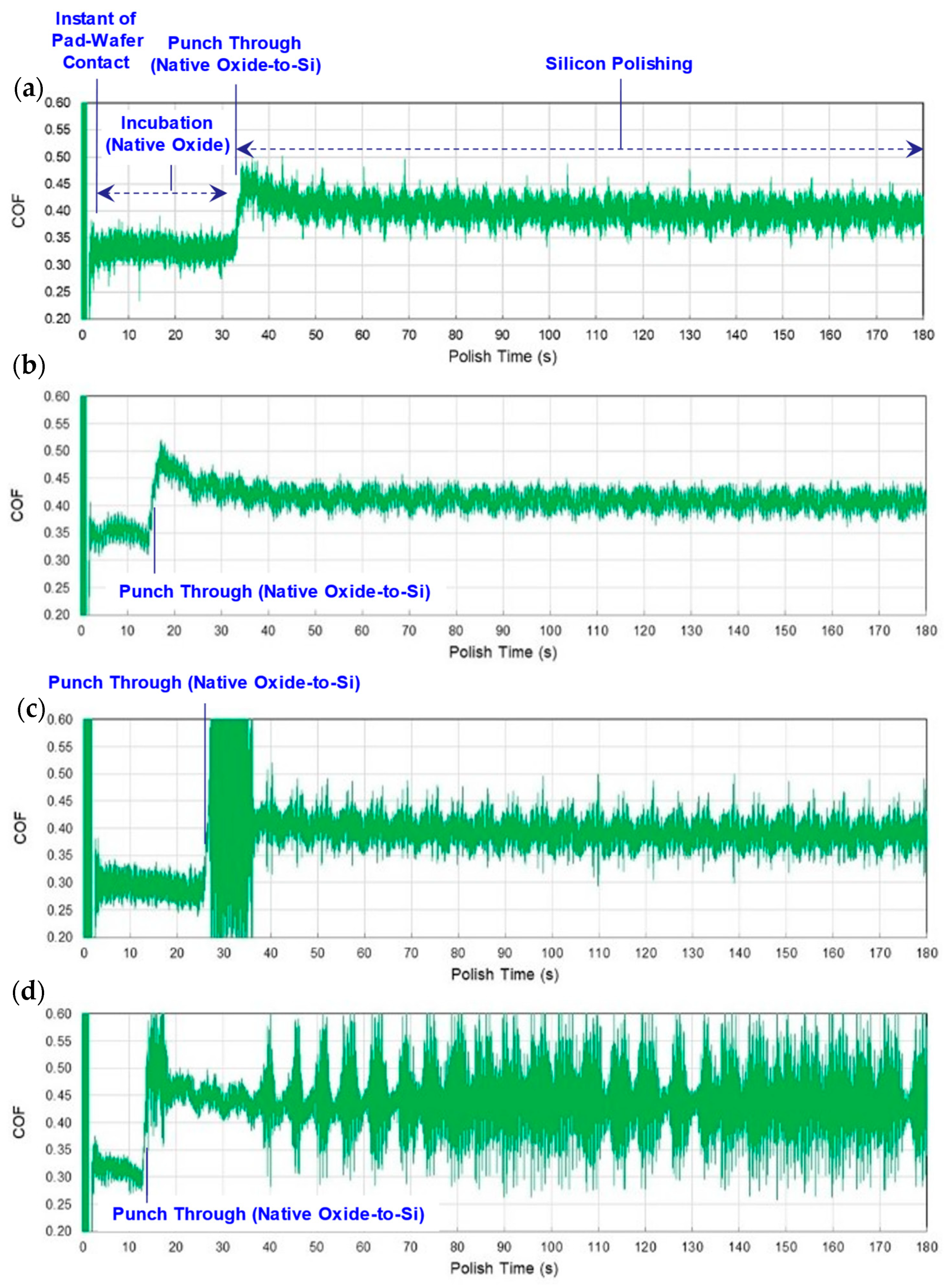
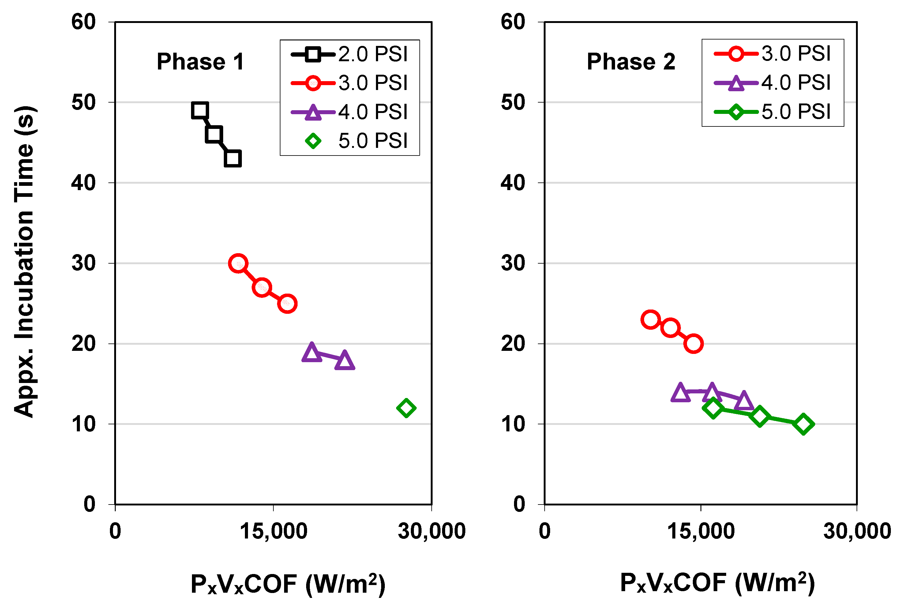
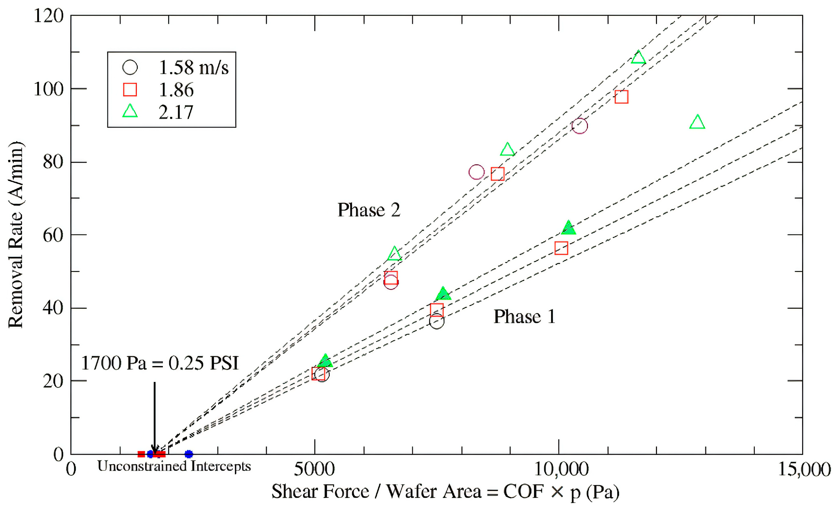
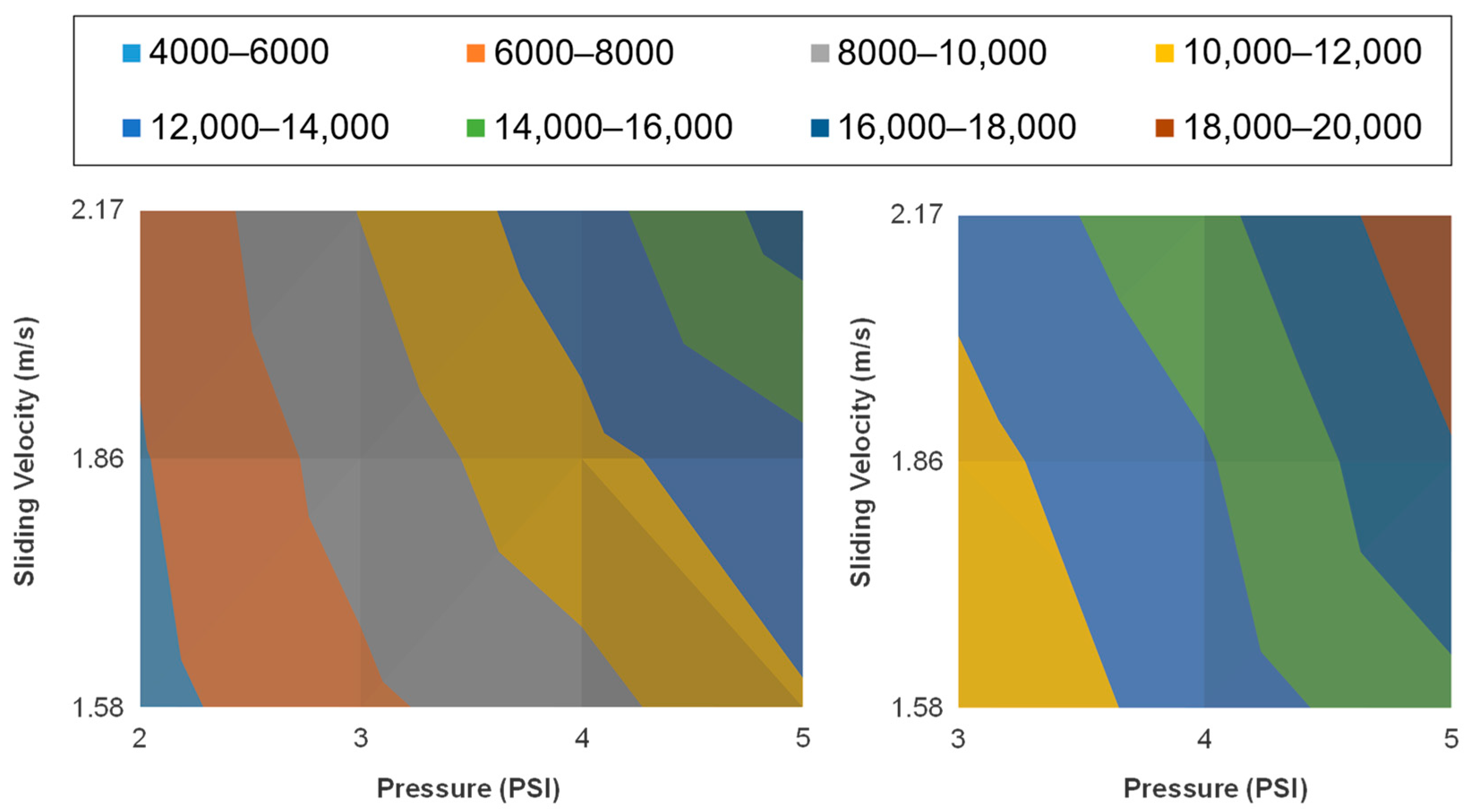
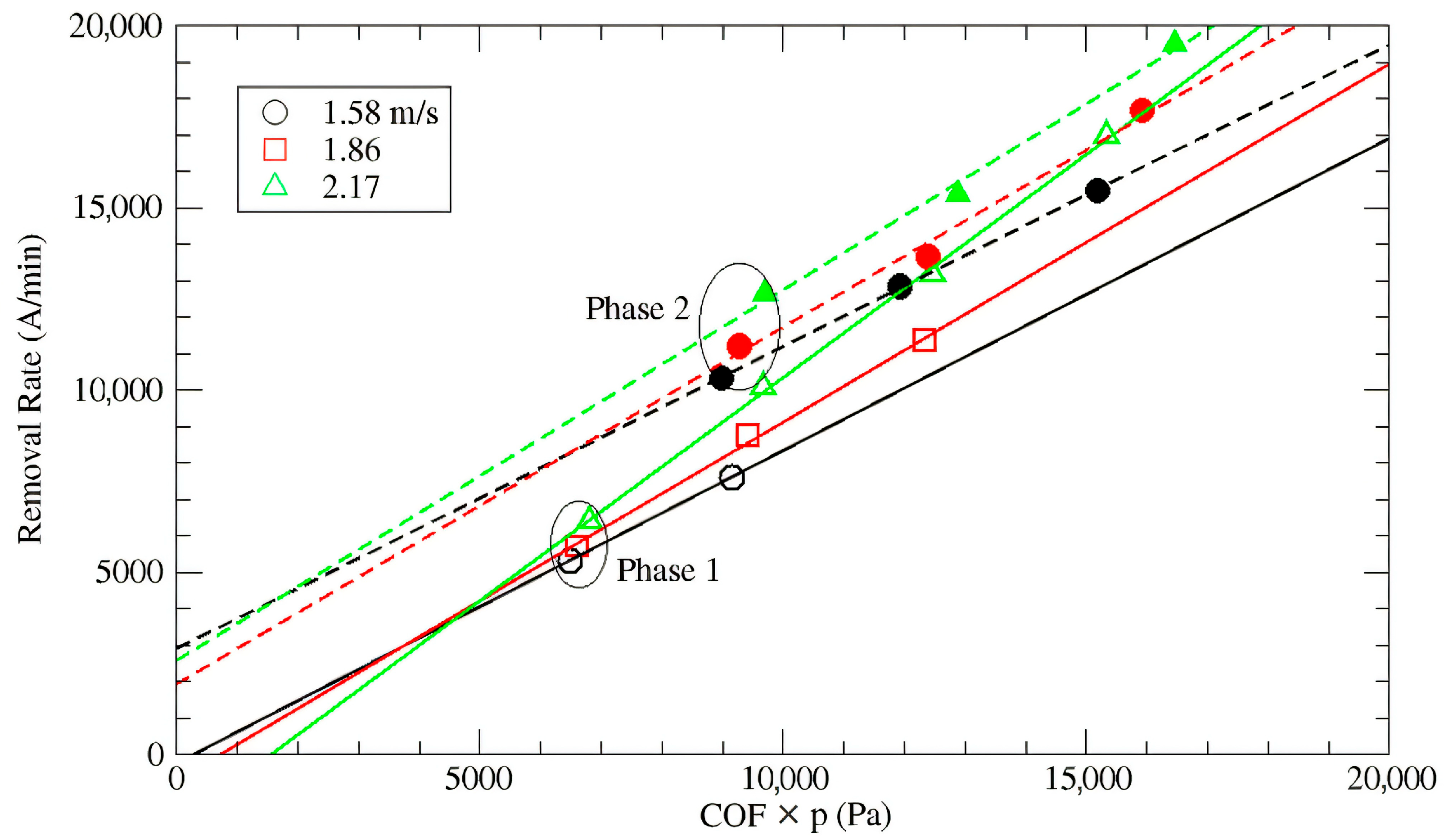
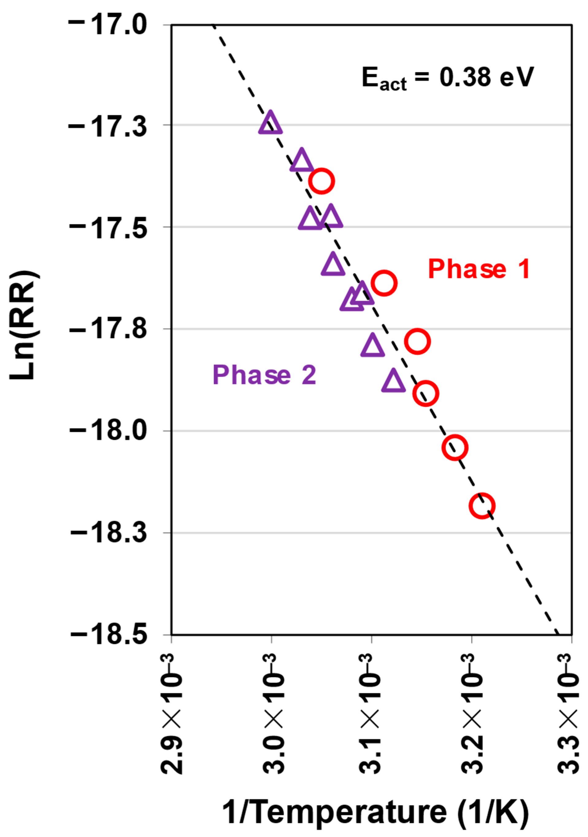
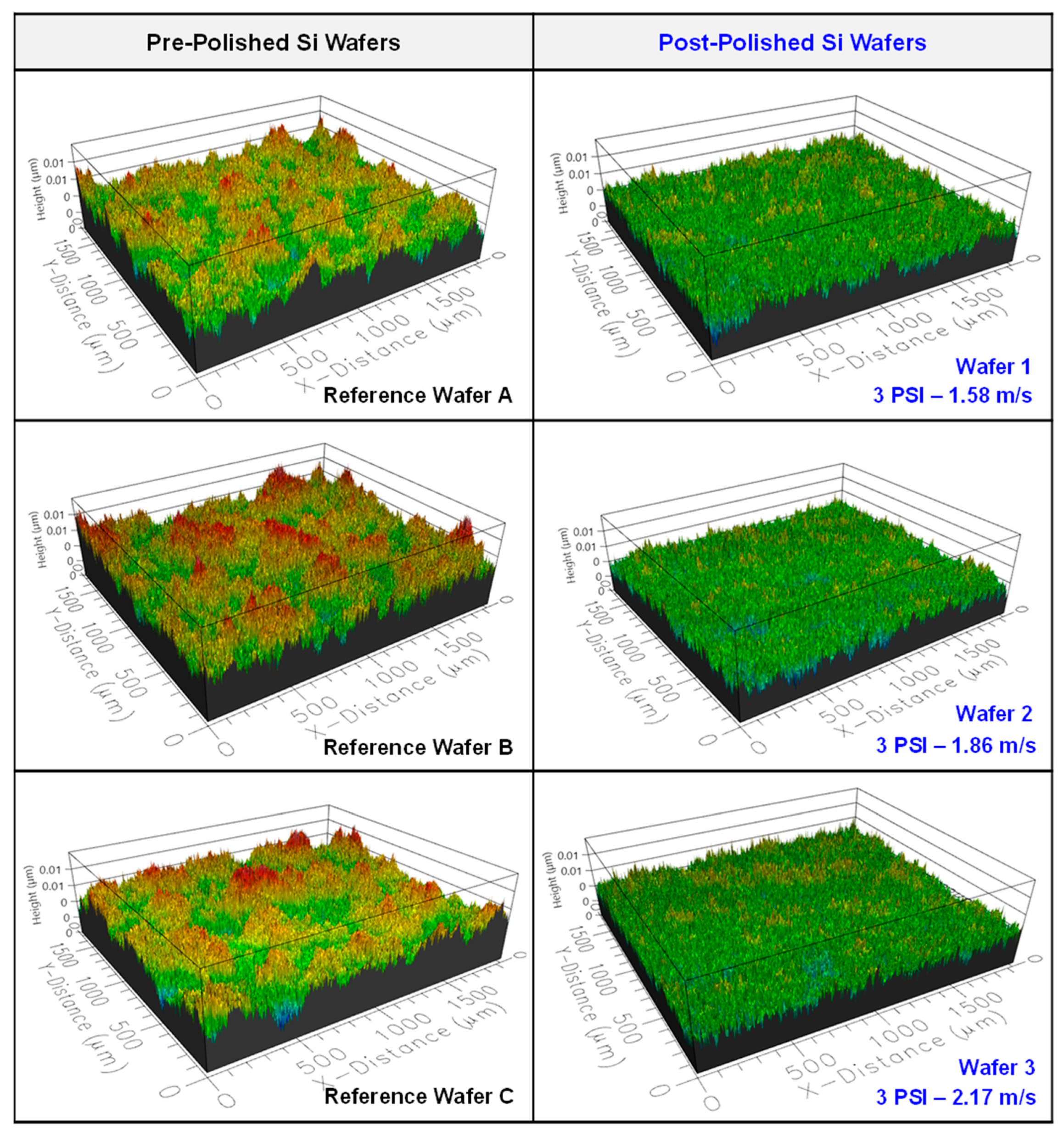
3.1. Native Oxide Polishing

While studying silicon CMP, its tribology and associated kinetics cannot be fully and accurately comprehended unless we understand what happens during the native oxide polishing that occurs first. We know that silicon polishing slurries have very poor native oxide removal rates [28], so one needs first to quantify the exact time when the entire native oxide layer is removed, thereby causing silicon to start being polished. In this study, we discovered that such a decoupling could be carried out by investigating polishing frictional phenomena in real time.
Previous studies have shown that the spectral analysis of shear force and COF can be implemented as an end-point detection (EPD) system to precisely, and in real time, monitor the progression and transition of the two films during CMP [37,38,39]. Sampurno et al. showed that the trends in blanket SiO2 and Ta/TaN wafer polishing were qualitatively similar to the COF exhibited in Ta/TaN clearing (i.e., the transition from Ta/TaN film to SiO2 film) during patterned wafer polishing [37]. The COF and shear force started at lower values with the Ta/TaN film. As the polished wafer surface started to transition from Ta/TaN to the subsequent SiO2 film, the COF and shear force increased by approx. 50% [37]. In separate studies, Mariscal et al. and Sampurno et al. employed the same technique as an EPD method for shallow trench isolation (STI) patterned wafer polishing [38,39]. In these cases, COF values increased by approx. 50% when the polishing process transitioned from the high-density plasma oxide film to the underlying silicon nitride layer [38,39].
In our present study, we also employed the same COF spectral analysis technique as an EPD method to identify the transition from the native oxide layer to the underlying bulk silicon material. Figure 1 shows how the COF—defined as the instantaneous ratio of shear force to normal force (i.e., Fx to Fz)—changes during the 3 min polishing process. The four examples (two from Phase 1 and two from Phase 2) highlight the exact time of native oxide clearing for a low P × V process (Figure 1a,c) as well as a relatively high P × V process (Figure 1b,d). Thankfully, the COF for native oxide polishing is significantly lower than that of silicon, which allows one to pinpoint when the native oxide is completely removed by employing the same COF spectral analysis method for EPD [38,39]. Naturally, the higher the value of P × V, the less time required for native oxide removal. Henceforth, we will refer to the time needed to punch through the native oxide layer as the “incubation time”, or tinc.
Figure 2 shows that, for Phase 1, tinc ranges between 49 s at the lowest polishing power density (i.e., P × V × COF) to 12 s at the highest polishing power density. This means that in 3 min, depending on the value of polishing power density, 27 to 7% of the time is spent punching through the native oxide. For Phase 2, tinc ranges between 23 and 10 s, corresponding to 13 to 6% of the entire polish time. Also note that in both phases, tinc is a much stronger function of P than it is of V, which indicates that the native oxide removal rate, which must be inversely proportional to tinc, should be highly non-Prestonian [35,39,40,41,42,43]. In the case of Figure 2 and all other figures that involve P and V, the values of P and V used are the actual values as measured by our polisher’s unique instrumentation and not just the setpoint values that our polisher’s controller also reports. Note that all other polishers used in high-volume manufacturing rely on the setpoint values the authors believe are less scientifically sound. In our case, for P, the setpoint values were roughly 6% lower than the actual measured values. For V, the difference was less than 2%.
Figure 3 shows how temperature reacts to polishing power density (i.e., P × V × COF) in Phases 1 and 2. Since pressures of 3, 4, and 5 PSI were common in both phases, a simple comparison of those three isobars indicates that platen heating successfully increased the mean pad temperature during the entire process by about 7 to 9 °C. This increase in process temperature is important, as it is manifested in the lower COF values seen in Figure 4 for Phase 2. A comparison of the same three isobars indicates that platen heating caused COF values to drop by approx. 11%. We believe this to be due to the thermoplastic properties of the VP6000®, as it will become softer, even though it may not reach the glass transition temperature, at the higher temperatures encountered in this study. For most thermoplastic CMP pads, the glass transition temperature (Tg) generally ranges from 32 to 70 °C [44], although values as high as 110 °C have also been reported for certain polyurethane formulations [45,46]. For the VP6000®, we measured Tg to be 99.3 °C (Figure 5). Although our measured pad temperatures do not reach such a high value, two aspects need to be emphasized: (1) Below the glass transition temperature, the elastic modulus of VP6000® drops by more than 30% between the range of temperatures encountered in our study (20 to 60 °C), causing dramatic pad softening, and (2) it is entirely conceivable for the actual temperature of the pad asperities contacting the wafer to be much higher than our measured mean pad surface temperatures. This has been reported in detail by Borucki [47], whose summit heating kinetic model has shown, albeit via simulation, that the asperity summit temperatures can exceed 200 °C.
Figure 4 summarizes how the COF behaves as a function of P and V in both Phase 1 and Phase 2. Several features are noteworthy. First, on average, the COF is 12% lower when platen heating is employed. This is likely due to further thermal softening of the pad at the elevated temperatures in Phase 2. Second, the COF values in the two phases differ only by a fixed vertical translation (or shift). This indicates that whatever the mechanisms are that cause the small observed variations in the COF with P and V, they are independent of temperature within the range of the experiment. Incidentally, the fact that, for a given phase, COF changes only slightly across a wide range of pressures and velocities indicates that, in this study, the dominant tribological mechanism is three-body-contact between the wafer, the nanoparticles, and the pad asperities (i.e., boundary lubrication) [31,34,35].
Knowing that about 18 Ǻ of native oxide is present atop prime silicon wafers when they have been stored in ambient conditions for several weeks or months [23,24,28], we can easily estimate that native oxide removal rates (Figure 6 and Figure 7) range from about 21 to 108 Ǻ/min. As implied by the data in Figure 2, removal rates are a strong function of P and somewhat dependent on T. Interestingly, V does not play a major role in material removal.
To help visualize the dependence of removal rate on P and to some extent on T, and its weak dependence on V, the data in Figure 6 can be plotted in the form of Lim–Ashby plots [48,49], with P and V as the abscissa and the ordinate, and the removal rate as the response surface (see Figure 7). The nearly vertical contours in both Phase 1 and Phase 2 help show the relative non-importance of V.
Consequently, the authors believe that a much better way of presenting the native oxide removal data is via the Shear Force Law (SFL) recently reported by Borucki et al. [50]. The SFL, which generalizes the classical version of Preston’s Law, can model both Prestonian removal behavior and most highly non-Prestonian behavior, which may occur in copper and tungsten CMP. The criterion for applying it is that when the removal rate is plotted against the measured wafer frictional shear force per unit area, the data should lie on or near rays, indexed by V, that emanate from a common intercept. When the intercept is on the vertical removal rate axis, evidence suggests that the intercept quantifies a combination of the static etch rate and the influence of pad fragments from conditioning. An intercept on the horizontal axis indicates the presence of a shear force threshold.
Figure 8 shows the same data as in Figure 6, except this time plotted per the SFL. We can see that for a given V, the rays (or half-lines) do indeed converge towards a common intercept on the horizontal axis. The intercept is at about 1700 Pa (0.25 PSI or 120 N total shear force) for Phases 1 and 2. The intercept in this case has been constrained to be common to both phases; however, even without this constraint, the mean intercepts for each phase are still nearly the same (see the blue and red dots on the horizontal axis). This suggests that while the removal rate clearly depends on temperature, the mechanism causing the threshold behavior is independent of temperature within the range of the experiment. The presence of a temperature-independent shear force threshold and the low observed removal rates suggest that native oxide removal by the slurry is predominantly mechanical (abrasive), not chemical.
In contrast, removal rates at 4 PSI and 1.86 m/s for the PE-TEOS silicon dioxide wafers are 8.9 and 10.5 Ǻ/min for Phases 1 and 2, respectively. At 5 PSI and 2.17 m/s, the values are 13.4 and 15.4 Ǻ/min for Phases 1 and 2, respectively. These values, when compared to those of native oxide at the same P × V settings, indicate an average PE-TEOS silicon dioxide to native oxide removal rate selectivity of 1:7. This suggests that when designing silicon polishing slurries to increase silicon-to-silicon dioxide removal rate selectivities, one cannot simply rely on experimentally obtained PE-TEOS silicon dioxide polish rates, as they underestimate the true silicon-to-native oxide removal selectivities by a factor of 7. This can cause problems in manufacturing processes involving wafer thinning that are needed for direct wafer bonding, as only having direct knowledge about how fast or how slow a particular slurry removes native oxide will allow one to optimize slurry performance.

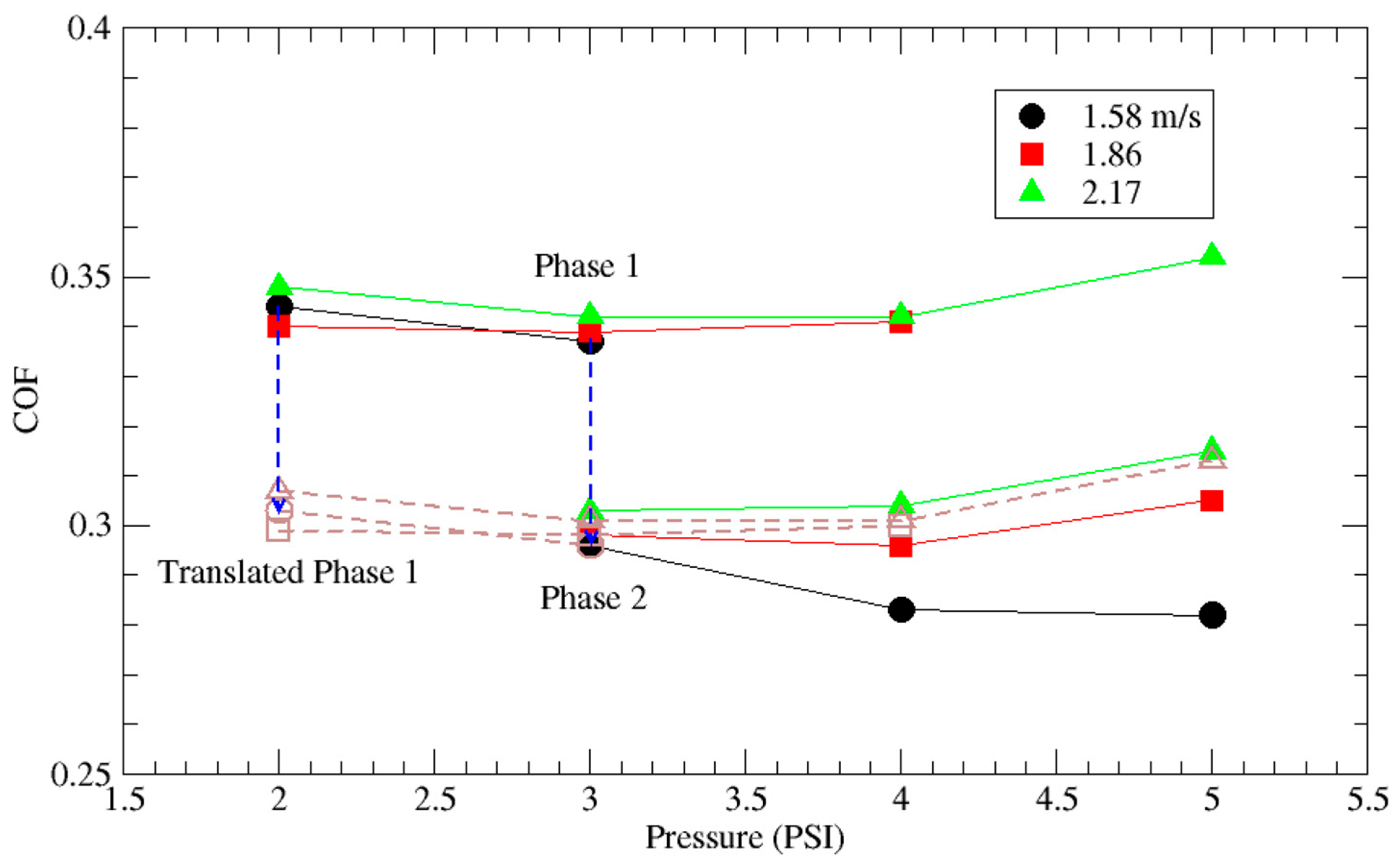
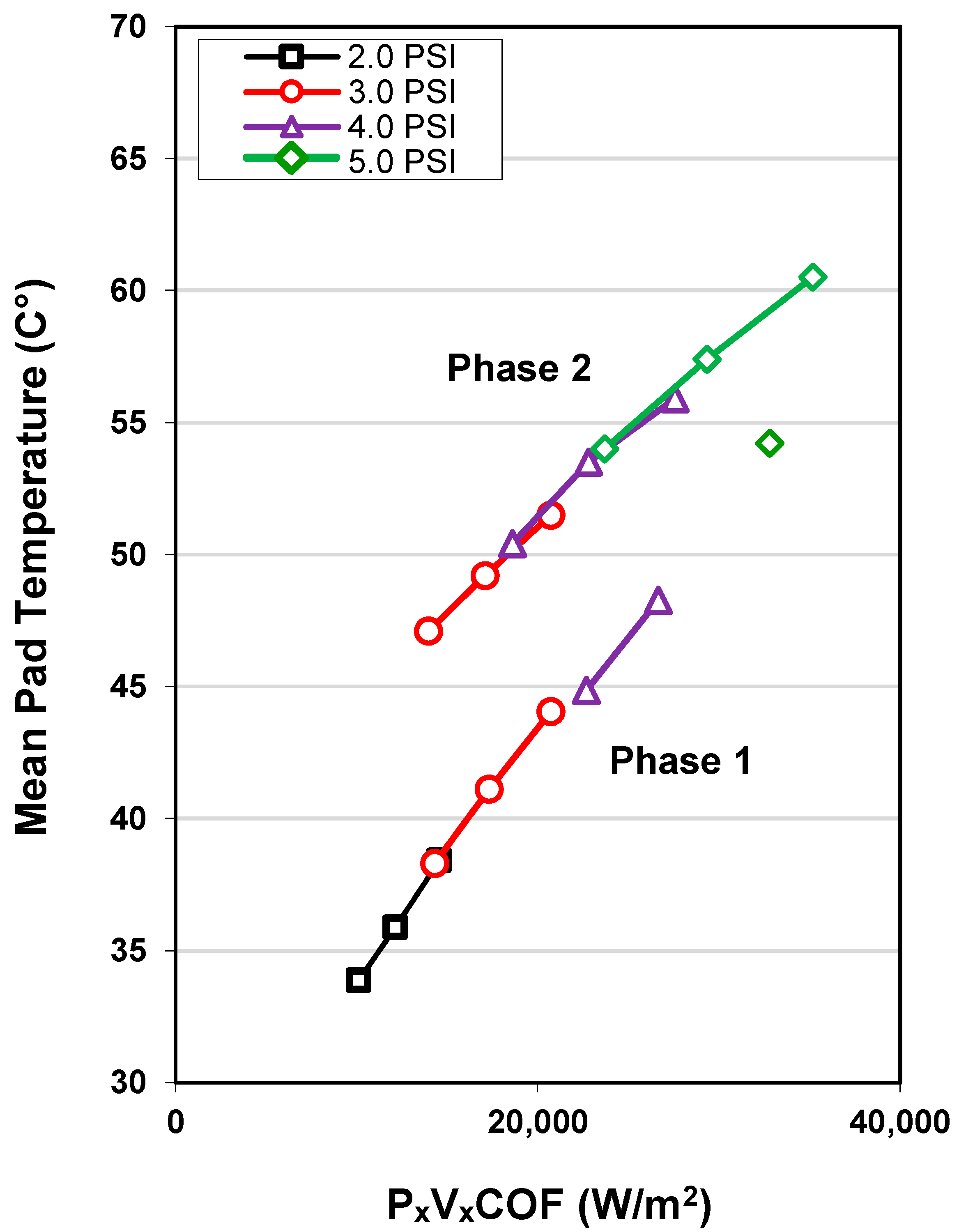
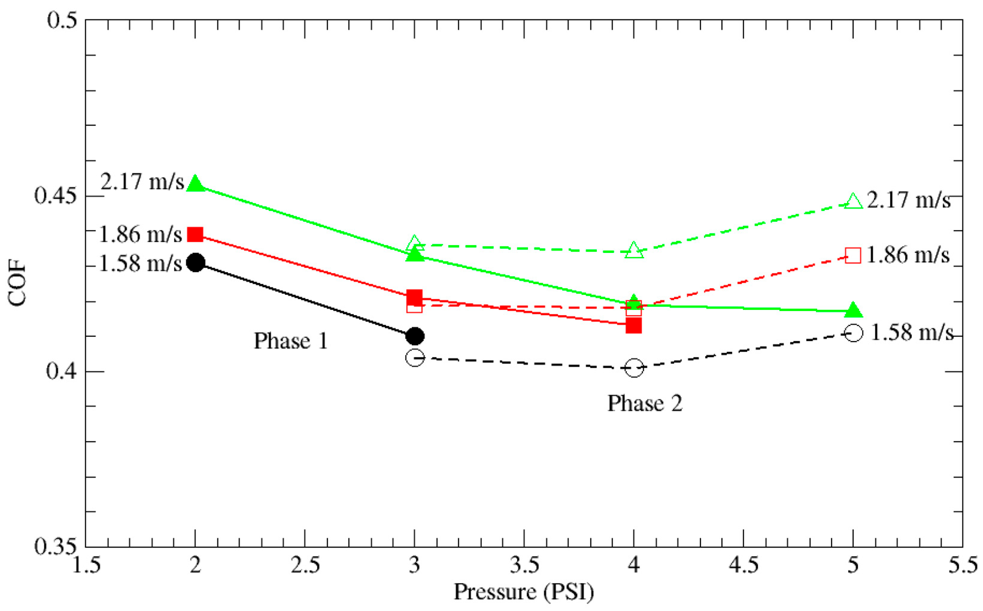
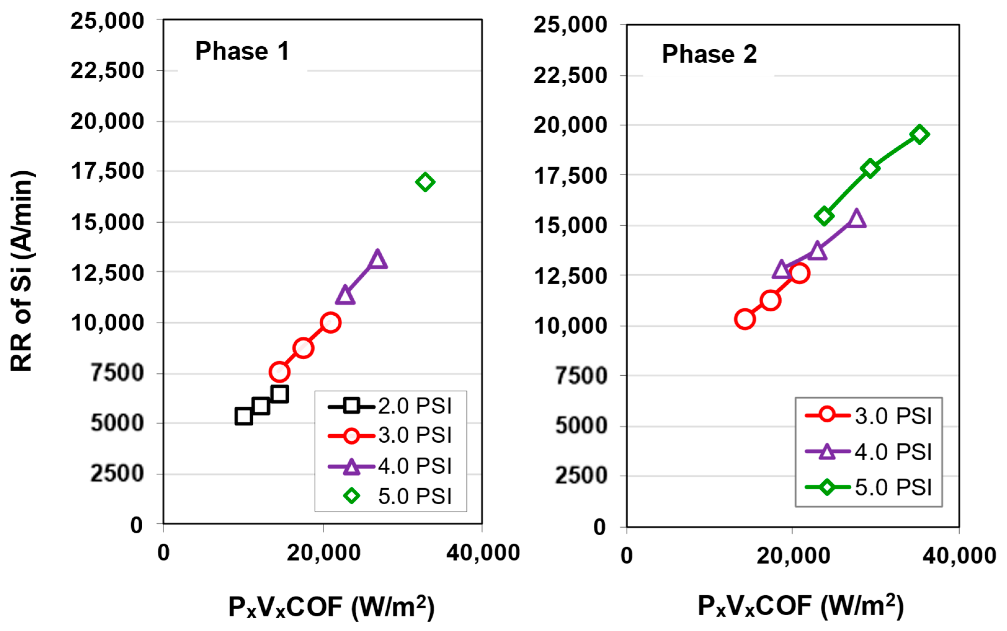
3.2. Silicon Polishing

Figure 9 shows how T is affected by polishing power density for Phases 1 and 2. The data correspond to the post-incubation interval of the polishing process, as it is during this interval that silicon is being polished. A simple comparison of the data points corresponding to 3, 4, and 5 PSI indicates that platen heating successfully increases the mean pad temperature during the post-incubation interval by about 5 to 8 °C. This rise in temperature is smaller than during the incubation period, as process temperatures tend to level off with increasing polish time.
Figure 10 shows the dependence of the COF during Si polishing on speed and pressure in Phases 1 and 2. Notably, the silicon COF does not evidence a downward shift in Phase 2 like it did for native oxide removal (Figure 6). The COF shift for native oxide and the lack of it for silicon polishing may have a simple origin. When a clean silicon surface is oxidized by room temperature exposure to air, the formed oxide has to occupy a volume 2.2 times that of the silicon consumed. This causes planar compressive stress in the oxide along the interface and is also a factor in the resulting roughness of the oxide surface. When platen heating is then applied, both materials expand. Still, the coefficient of thermal expansion (CTE) of silicon (2.6–3.3 × 10⁻⁶/°K) is more than ten times higher than the CTE of thin-film silicon dioxide (0.24 × 10⁻⁶/°K) [51]. Thermal expansion of the silicon therefore relieves some of the compressive strain in the surface oxide. Considering that platen heating is the only difference between Phase 1 and Phase 2, during native oxide polishing this may be the cause of the COF reduction. COF results for Phase 2 also rule out certain other explanations. For example, the oxide COF drop cannot be a lubrication effect due to pad softening because it should then occur during Si polishing, but it does not. Relief of some of the compressive strain in the native oxide may also contribute to the increase in the removal rate in Phase 2 (Figure 8). After clearing, only silicon is being polished using the same consumables and no comparable mechanism is present. The fact that, for a given phase, COF during silicon polishing changes only slightly across a wide range of pressures and velocities indicates that, similar to native oxide polishing, we are operating in boundary lubrication.
Figure 11 and Figure 12 show how silicon removal rates change with polishing power density (i.e., COF × P × V) for Phases 1 and 2. The Lim–Ashby plots of Figure 12 show removal rate contours that are more or less equally dependent on V and P, but both systems are far from being Prestonian. When comparing the 3, 4, and 5 PSI data points of Phase 1 to those of Phase 2, we observe that platen heating increases removal rates by an average of only 25%, which is not dramatic.
Figure 13 shows the silicon removal rate for Phases 1 and 2 plotted against the shear force per unit area. Unlike native oxide removal (Figure 8), silicon Phase 1 and Phase 2 do not share a distinctive shear force threshold. Since platen heating shifts the silicon removal rates upward at about the same slope in Phase 2 relative to Phase 1, removal rates are roughly 165 to 255 times larger for silicon removal than for native oxide removal using the same consumables, and the mechanism for silicon appears to be dominantly chemical.
Given that we continuously acquired real-time pad temperature data during polishing, we were able to construct Arrhenius plots for silicon removal, as shown in Figure 14. The temperatures used in constructing the plots were the mean pad temperature (T) during the post-incubation intervals of the 3 min polish for each P and V. We can see that in both phases, the extracted apparent activation energy is not very large. Considering the scatter in the data, one can assume it to be around 0.38 eV, which explains the dependence (albeit, not very pronounced) of removal rate to temperature shown in Figure 11 and Figure 13. This dependence on temperature can also be partially explained by pad softening at higher temperatures. The authors believe this to be the first time that polishing (CMP) of native oxide and silicon has been rigorously studied and reported in terms of its tribological, thermal, and kinetic attributes in the open literature.
Figure 15 shows selected examples of the Si wafers’ pre-polished and post-polished surface topography. The scales on all graphs are kept the same to allow one to observe the surface quality differences better. Sa (mean difference in height from the mean plane) and Sq (equivalent to the standard deviation of height distribution) data are summarized in Figure 16. Error bars represent 1σ values. Post-polished Si wafers reduced wafer surface roughness by approx. 30% in both Sa and Sq. We can attribute the higher surface roughness of pre-polished wafers to a relatively rough native oxide layer that grows in generally uncontrolled storage environments. As discussed earlier, the high roughness of the native oxide layer is also caused by planar compressive stress, as the oxide that is formed must occupy a volume 2.2 times that of the amount of silicon consumed when a clean silicon surface is oxidized by exposure to room-temperature air. In our case, the CMP process that we developed removes the native oxide and proceeds to planarize the surface, thereby achieving a near-mirror finish quality.
An interesting observation can be made when comparing the post-incubation COF time traces from Phase 1 to Phase 2. In CMP, the slurry abrasive particles and the pad make physical contact. As such, multiple high-frequency stick–slip events cause vibrations within the wafer–slurry–pad–polisher system. These vibrations manifest as shear and normal force fluctuations during polishing [52]. Such fluctuations can be quantified by calculating their variance values. A previous publication reported that the variance of shear forces correlated well with the extent of vibrations during CMP [37,38,39]. Figure 17 summarizes the average variances of shear and normal forces for both phases. The error bars represent 1σ. Figure 17 shows that the higher pad temperature associated with Phase 2 causes significantly higher variances in shear and normal force by as much as 6X and 2X, respectively, compared to those of Phase 1.
While platen heating in Phase 2 increases removal rates by an average of 25% compared to Phase 1, it also causes significantly higher levels of polishing vibration. Such vibrations may contribute to an increase in wafer-level defects. Even though the authors did not study the impact on defects, we believe higher platen temperatures may lessen any benefits of removal rates [52].

4. Conclusions

To understand the silicon polishing process, we first had to set out to de-couple the study of silicon removal rate from that of its native oxide, as the latter acted as a natural hindrance to the overall polishing process. We then proceeded to systematically investigate the tribological, thermal, kinetic, and surface-quality characteristics of chemical mechanical polishing of 300 mm p-type <100> prime silicon wafers (and their native oxide) at various pressures, sliding velocities, and platen temperatures. For native oxide removal, we showed that the dominant tribological mechanism was boundary lubrication with intimate three-body contact between the polyurethane pad, the wafer, and the silica nanoparticles that remained suspended in the slurry. With the aid of real-time frictional data, for each pressure and velocity combination tested, we identified the exact time corresponding to the total removal of the native oxide and the onset of silicon polishing. As expected, this “incubation time” decreased with increasing P × V and external platen heating. This allowed us to separately characterize the removal rate of native oxide from that of silicon.
For native oxide, while the removal rate depended on temperature (either resulting from higher values of P × V or otherwise induced using an external heat exchanger for the platen), the presence of a temperature-independent shear force threshold and the low observed removal rates suggested that native oxide removal by the slurry was dominantly mechanical. In contrast, for silicon polish, the absence of a distinctive shear force threshold and the fact that, for the same set of consumables, removal rates were more than 200 times larger for silicon than for native oxide suggested a dominantly chemical process with an apparent activation energy of about 0.38 eV.
We also proved the dominant tribological mechanism for silicon polish to be boundary lubrication (similar to the native oxide case). By also polishing PE-TEOS silicon dioxide control wafers, we were able to confirm that the removal rate selectivity between native oxide and PE-TEOS silicon dioxide was around 1:7. This underscored the importance of being able to measure native oxide removal rates directly and designing silicon CMP slurries that could remove both the native oxide and the underlying silicon, albeit through different primary removal rate mechanisms.
When comparing the post-incubation COF time traces for heated vs. non-heated platens, the former caused significantly higher shear and normal force variances. This was likely due to the pad’s thermal softening due to the higher process temperatures. While higher temperatures increased removal rates to a certain extent, one must be cautious of the adverse effects of such extreme vibrations, such as an increase in wafer-level defects.

Author Contributions

Conceptualization, A.P. and G.W.; methodology, Y.S. and A.P.; software, M.Y., C.Y., Y.S. and L.B.; validation, M.Y., C.Y. and Y.S.; formal analysis, M.Y, C.Y., Y.S., L.B. and A.P.; investigation, C.Y., M.Y., Y.S., L.B. and J.K.; resources, G.W. and A.P.; data curation, M.Y., C.Y. and Y.S.; writing—original draft preparation, A.P., M.Y., C.Y. and Y.S.; writing—review and editing, M.Y., C.Y., A.P., L.B. and Y.S.; visualization, M.Y., C.Y., L.B. and Y.S.; supervision, Y.S and A.P.; project administration, A.P. and Y.S.; funding acquisition, A.P. and G.W. All authors have read and agreed to the published version of the manuscript.

Funding

This research received no external funding.

Data Availability Statement

The original contributions presented in this study are included in the article. Further inquiries can be directed to the corresponding author.

Conflicts of Interest

Authors Michelle Yap, Catherine Yap, Yasa Sampurno, Len Borucki and Ara Philipossian were employed by the company Araca, Inc. Author Glenn Whitener was employed by the company Fujimi Corporation. The remaining authors declare that the research was conducted in the absence of any commercial or financial relationships that could be construed as a potential conflict of interest.

References

  1. Steigerwald, J.; Murarka, S.; Gutmann, R. Chemical Mechanical Planarization of Microelectronic Materials; Wiley: New York, NY, USA, 2008. [Google Scholar]
  2. Oliver, M.R. Chemical-Mechanical Planarization of Semiconductor Materials; Springer: New York, NY, USA, 2003. [Google Scholar]
  3. Chen, C.; Shu, L.; Lee, S. Mechano-Chemical Polishing of Silicon Wafers. J. Mater. Process. Technol. 2003, 140, 373–378. [Google Scholar] [CrossRef]
  4. Wang, Y.G.; Zhang, L.C.; Biddut, A. Chemical Effect on the Material Removal rate in the CMP of Silicon Wafers. Wear 2011, 270, 312–316. [Google Scholar] [CrossRef]
  5. Srivastava, M.; Singh, J.; Mishra, D.; Singh, R. Review on the Various Strategies Adopted for the Polishing of Silicon Wafer—A Chemical Perspective. Mater. Today Proc. 2022, 63, 62–68. [Google Scholar] [CrossRef]
  6. Hong, J.; Niu, X.; Liu, Y.; Wang, C.; Zhang, B.; Sun, M.; Wang, J.; Han, L.; Zhang, W. Removal Rate and Surface Quality of the GLSI Silicon Substrate during the CMP Process. Microelectron. Eng. 2017, 168, 76–81. [Google Scholar] [CrossRef]
  7. Teichert, C.; MacKay, J.F.; Savage, D.E.; Lagally, M.G.; Brohl, M.; Wagner, P. Comparison of Surface Roughness of Polished Silicon Wafers Measured by Light Scattering Topography, Soft-X-Ray Scattering, and Atomic-force Microscopy. Appl. Phys. Lett. 1995, 66, 2346–2348. [Google Scholar] [CrossRef]
  8. Yasseen, A.A.; Mourla, N.J.; Mehregan, M. Chemical-Mechanical Polishing for Polysilicon Surface Micromachining. J. Electrochem. Soc. 1997, 144, 237. [Google Scholar] [CrossRef]
  9. Park, J.; Prasad, Y.; Kang, Y.; Kim, I.; Hong, Y.; Han, S.; Yun, S.; Yoo, B.; Busnaina, A. Effect of Polysilicon Wettability on Polishing and Organic Defects during CMP. J. Electrochem. Soc. 1999, 156, H869. [Google Scholar] [CrossRef]
  10. Chao, T.; Penigalapati, D.; Yang, J.; Huang, H.; Koli, D. The Role of Polysilicon Slurry and Its Application in 7nm CMP. ECS Trans. 2017, 77, 227. [Google Scholar] [CrossRef]
  11. Jeon, S.; Hong, J.; Hong, S.; Kanade, C.; Park, K.; Seok, H.; Kim, H.; Lee, S.; Kim, T. Investigation of Abrasive-free Slurry for Polysilicon Buffing Chemical Mechanical Planarization. Mater. Sci. Semicond. Process. 2021, 128, 105755. [Google Scholar] [CrossRef]
  12. Joshi, V.; Orlov, A.; Snider, G. Controlled Chemical Mechanical Polishing of Polysilicon and Silicon Dioxide for single-electron Device. J. Vac. Sci. Technol. A 2007, 25, 1034–1037. [Google Scholar] [CrossRef]
  13. Pirayesh, H.; Cadien, K. The Effect of Slurry Properties on the CMP Removal Rate of Boron Doped Polysilicon. ECS J. Solid State Sci. Technol. 2016, 5, P233. [Google Scholar] [CrossRef]
  14. Huang, H.; Koli, D.; Zhang, J.; Tsai, S.; Chao, T.; Lu, Y.; Kim, H.; Fang, Q.; Lu, W. New CMP Processes Development and Challenges for 7nm and Beyond. In Proceedings of the 2018 China Semiconductor Technology International Conference (CSTIC), Shanghai, China, 11–12 March 2018; pp. 1–5. [Google Scholar]
  15. Pirayesh, H.; Cadien, K. High Rate Chemical Mechanical Polishing of Boron-Doped Polycrystalline Silicon. ECS J. Solid State Sci. Technol. 2014, 3, P213. [Google Scholar] [CrossRef]
  16. Bao, S.; Wang, Y.; Lina, K.; Zhang, L.; Wang, B.; Sasangka, W.; Lee, K.; Chua, S.; Michel, J.; Fitzgerald, E.; et al. A Review of Silicon-based Wafer Bonding Processes, an Approach to Realize the Monolithic Integration of Si-CMOS and III–V-on-Si Wafers. J. Semicond. 2021, 42, 023106. [Google Scholar] [CrossRef]
  17. Park, S.; Yoon, S.; Kim, H.; Jeong, H. A Hybrid Polysilicon Planarization for Suppressing Dishing Defects. J. Mater. Process. Technol. 2012, 212, 2635–2641. [Google Scholar] [CrossRef]
  18. Masteika, V.; Kowal, J.; Braithwaite, N.; Rogers, T. A Review of Hydrophilic Silicon Wafer Bonding. ECS J. Solid State Sci. Technol. 2014, 3, Q42. [Google Scholar] [CrossRef]
  19. He, R.; Fujino, M.; Yamauchi, A.; Suga, T. Novel Hydrophilic SiO2 Wafer Bonding Using Combined Surface-activated Bonding Technique. Jpn. J. Appl. Phys. 2015, 54, 030218. [Google Scholar] [CrossRef]
  20. Wang, X.; Wang, C.; Zhu, M.; Zhou, J.; Luo, C.; Chen, Z.; Yang, X.; Wang, H.; Zhang, X. Insight on Surface Changes Post Chemical Mechanical Polishing (CMP) of the Silicon Substrate by Adding Polyoxyethylene Ether. ECS J. Solid State Sci. Technol. 2023, 12, 114005. [Google Scholar] [CrossRef]
  21. Philipossian, A. The Activity of HF/H2O Treated Silicon Surfaces in Ambient Air Before and After Gate Oxidation. J. Electrochem. Soc. 1992, 139, 2956. [Google Scholar] [CrossRef]
  22. Morita, M.; Ohmi, T.; Hasegawa, E.; Kawakami, M.; Ohwada, M. Growth of Native Oxide on a Silicon Surface. J. Appl. Phys. 1990, 68, 1272–1281. [Google Scholar] [CrossRef]
  23. Taft, E. Growth of Native Oxide on Silicon. J. Electrochem. Soc. 1998, 135, 1022. [Google Scholar] [CrossRef]
  24. Grundner, M.; Jacob, H. Investigations on Hydrophilic and Hydrophobic Silicon (100) Wafer Surfaces by X-ray Photoelectron and High-resolution Electron Energy Loss-spectroscopy. Appl. Phys. A 1986, 39, 73–82. [Google Scholar] [CrossRef]
  25. Raider, S.; Fitsch, R.; Palmer, M. Oxide Growth on Etched Silicon in Air at Room Temperature. J. Electrochem. Soc. 1975, 122, 413. [Google Scholar] [CrossRef]
  26. Li, F.; Balazs, M.; Anderson, S. Effects of Ambient and Dissolved Oxygen Concentration in Ultrapure Water on Initial Growth of Native Oxide on a Silicon (100) Surface. J. Electrochem. Soc. 2005, 152, G669. [Google Scholar] [CrossRef]
  27. Morita, M.; Ohmi, T.; Hasegawa, E.; Kawakami, M.; Suma, K. Control Factor of Native Oxide Growth on Silicon in Air or in Ultrapure Water. Appl. Phys. Lett. 1989, 55, 562–564. [Google Scholar] [CrossRef]
  28. Shin, W.; Cho, H.; Lee, H.; Jeong, H. Effect of Native Oxide on Polycrystalline Silicon CMP. J. Korean Phys. Soc. 2009, 54, 1077. [Google Scholar] [CrossRef]
  29. Venkatesh, R.; Prasad, Y.; Kwon, T.; Kang, Y.; Park, J. Effect of Alkaline pH on Polishing and Etching of Single and Polycrystalline Silicon. Jpn. J. Appl. Phys. 2012, 51, 071301. [Google Scholar] [CrossRef]
  30. Park, J.; Venkatesh, R.; Kwon, T. Material Removal Mechanism of Single and Polycrystalline Silicon in Alkaline Slurry. ECS Trans. 2013, 52, 545. [Google Scholar] [CrossRef]
  31. Sampurno, Y. Fundamental Consumables Characterization of Advanced Dielectric and Metal Chemical Mechanical Planarization Processes. Ph.D. Dissertation, University of Arizona, Tucson, AZ, USA, 2008. [Google Scholar]
  32. APD-800 Prime® Polisher and Tribometer for R&D and Low-Volume Manufacturing. Available online: https://aracainc.com/wp-content/uploads/2023/10/APD-800-Prime-Brochure-2023.pdf (accessed on 28 October 2024).
  33. Borucki, L.; Sampurno, Y.; Philipossian, A. Pad-Wafer-Slurry Interface Information from Force Data. ECS J. Solid State Sci. Technol. 2019, 8, P3133–P3144. [Google Scholar] [CrossRef]
  34. Meled, A. Optimization of Polishing Kinematics and Consumables During Chemical Mechanical Planarization Processes. Ph.D. Dissertation, University of Arizona, Tucson, AZ, USA, 2011. [Google Scholar]
  35. Han, R. Fundamental Characterization of Chemical Mechanical Planarization Relating to Slurry Dispensing and Conditioning Method. Ph.D. Dissertation, University of Arizona, Tucson, AZ, USA, 2017. [Google Scholar]
  36. Polar Series Accel 500 LC Cooling/Heating Recirculating Chillers. Available online: https://www.thermofisher.com/order/catalog/product/223322100 (accessed on 28 October 2024).
  37. Sampurno, Y.; Gu, X.; Nemoto, T.; Zhuang, Y.; Teramoto, A.; Philipossian, A.; Ohmi, T. End-Point Detection of Ta/TaN Chemical Mechanical Planarization via Forces Analysis. Jpn. J. Appl. Phys. 2010, 49, 05FC01. [Google Scholar] [CrossRef]
  38. Sampurno, Y.; Sudargho, F.; Zhuang, Y.; Ashizawa, T.; Morishima, H.; Philipossian, A. Pattern Evolution in Shallow Trench Isolation Chemical Mechanical Planarization via Real-Time Shear and Down Forces Spectral Analyses. Microelectron. Eng. 2011, 88, 2857–2861. [Google Scholar] [CrossRef]
  39. Mariscal, J.; McAllister, J.; Sampurno, Y.; Suarez, J.; O’Neill, M.; Zhou, H.; Grief, M.; Slutz, D.; Philipossian, A. Tribological, Thermal and Kinetic Characterization of SiO2 and Si3N4 Polishing for STI CMP on Blanket and Patterned Wafers. ECS J. Solid State Sci. Technol. 2020, 9, 044008. [Google Scholar] [CrossRef]
  40. Preston, F.W. The Theory and Design of Plate Glass Polishing Machines. J. Soc. Glass Technol. 1927, 11, 214–256. [Google Scholar]
  41. Zhao, B.; Shi, E.G. Chemical Mechanical Polishing: Threshold Pressure and Mechanism. Electrochem. Solid State Lett. 1999, 2, 145–147. [Google Scholar] [CrossRef]
  42. Tseng, W.T.; Wang, Y.L. Re-examination of Pressure and Speed Dependences of Removal Rate during Chemical-Mechanical Polishing Processes. J. Electrochem. Soc. 1997, 144, L15. [Google Scholar] [CrossRef]
  43. Shi, E.G.; Zhao, B. Ordered Mesoporous Non-Oxide Materials. Appl. Phys. A 1997, 67, 249. [Google Scholar] [CrossRef]
  44. Sampurno, Y.; Borucki, L.; Zhuang, Y.; Misra, S.; Holland, K.; Boning, D.; Philipossian, A. Characterization of Thermoset and Thermoplastic Polyurethane Pads and Molded and Machined Grooving Methods for Oxide CMP Applications. Thin Solid Film. 2009, 517, 1719–1726. [Google Scholar] [CrossRef]
  45. Chen, T.; Chui, J.; Shieh, T. Glass Transition Behaviors of a Polyurethane Hard Segment based on 4,4‘-Diisocyanatodiphenylmethane and 1,4-Butanediol and the Calculation of Microdomain Composition. Macromolecules 1997, 30, 5068–5074. [Google Scholar] [CrossRef]
  46. Pugar, J.; Childs, C.; Huang, C.; Haider, K.; Washburn, N. Elucidating the Physicochemical Basis of the Glass Transition Temperature in Linear Polyurethane Elastomers with Machine Learning. J. Phys. Chem. B 2020, 124, 9722–9733. [Google Scholar] [CrossRef] [PubMed]
  47. Borucki, L.; Sampurno, Y.; Philipossian, A. A New Summit Heating Kinetic Model for Copper and Tungsten CMP. In Proceedings of the Symposium on Chemical-Mechanical Planarization (CAMP), Lake Placid, NY, USA, 11−14 August 2021. [Google Scholar]
  48. Lim, S.; Ashby, M. Wear-mechanism Maps. Acta Metall. 1987, 35, 1–24. [Google Scholar] [CrossRef]
  49. Williams, J. Wear Modeling: Analytical, Computational and Mapping: A Continiuum Mechanics Approach. Wear 1999, 225, 1–17. [Google Scholar] [CrossRef]
  50. Borucki, L.; Sampurno, Y.; Philipossian, A. The Shear Force Law: A Guide to Modeling CMP Removal Rates. ECS J. Solid State Sci. Technol. 2023, 12, 044003. [Google Scholar] [CrossRef]
  51. Tsou, C.; Huang, Y.S.; Li, H.C.; Lai, T.H. Determination of Thermal Expansion Coefficient of Thermal Oxide. Sens. Mater. 2005, 17, 441–451. [Google Scholar]
  52. Philipossian, A.; Sampurno, Y.; Redeker, F.; Cahue, K.; Keleher, J. Slurry Activation for Enhanced Surface Redox Reactions in CMP. Solid State Phenom. 2021, 346, 311–317. [Google Scholar] [CrossRef]
Figure 1. Time traces of COF: (a) Phase 1 at 3 PSI—1.58 m/s, (b) Phase 1 at 5 PSI—2.17 m/s, (c) Phase 2 at 3 PSI—1.58 m/s, (d) Phase 2 at 5 PSI—2.17 m/s.
Electronicmat 06 00001 g001
Figure 2. Incubation times (tinc) as a function of power density for native oxide polishing: Phase 1 (left), Phase 2 (right).
Electronicmat 06 00001 g002
Figure 3. Mean pad temperature as a function of power density for native oxide polishing.
Electronicmat 06 00001 g003
Figure 4. COF as a function of P for each V for native oxide polishing during tinc in Phase 1 (top solid curves) and Phase 2 (bottom solid curves). A copy of the Phase 1 data has been translated (shifted) downward (dashed curves) to show the relationship of the Phase1 data to the Phase 2 data.
Electronicmat 06 00001 g004
Figure 5. Dynamic storage modulus, loss modulus, and tan δ of the VP6000® pad.
Electronicmat 06 00001 g005
Figure 6. Removal rate of native oxide vs. polishing power density: Phase 1 (left), Phase 2 (right).
Electronicmat 06 00001 g006
Figure 7. Lim–Ashby plots for native oxide removal rates: Phase 1 (left), Phase 2 (right).
Electronicmat 06 00001 g007
Figure 8. Removal rate of native oxide vs. actual shear force per unit area.
Electronicmat 06 00001 g008
Figure 9. Mean pad temperatures as a function of power density for silicon polishing.
Electronicmat 06 00001 g009
Figure 10. COF of silicon polishing—abscissa in linear scale: Phase 1 (solid curves), Phase 2 (dashed curves).
Electronicmat 06 00001 g010
Figure 11. Average removal rates during silicon polishing: Phase 1 (left), Phase 2 (right).
Electronicmat 06 00001 g011
Figure 12. Lim–Ashby plots for silicon removal rates: Phase 1 (left), Phase 2 (right).
Electronicmat 06 00001 g012
Figure 13. Removal rate of silicon vs. actual shear force per unit area.
Electronicmat 06 00001 g013
Figure 14. Arrhenius plots for silicon polishing.
Electronicmat 06 00001 g014
Figure 15. Surface microscopy of pre-polished and post-polished Si wafers.
Electronicmat 06 00001 g015
Figure 16. Surface roughness of pre-polished and post-polished Si wafers.
Electronicmat 06 00001 g016
Figure 17. Average variances of shear force and normal force.
Electronicmat 06 00001 g017
Disclaimer/Publisher’s Note: The statements, opinions and data contained in all publications are solely those of the individual author(s) and contributor(s) and not of MDPI and/or the editor(s). MDPI and/or the editor(s) disclaim responsibility for any injury to people or property resulting from any ideas, methods, instructions or products referred to in the content.

