Article

Characterization of Organic Conductive Materials as an Ecological Solution for RF Applications

Association Professorship of Microwave Engineering, Technical University of Munich, 80333 Munich, Germany
*
Author to whom correspondence should be addressed.
Electron. Mater. 2022, 3(4), 265-280; https://doi.org/10.3390/electronicmat3040023
Submission received: 13 July 2022 / Revised: 23 August 2022 / Accepted: 7 September 2022 / Published: 26 September 2022

Abstract

:
The use of nonmetallic conductor materials in RF applications has recently become a highlighted issue when it comes to sustainability in the electronics industry, mainly because of the waste problems associated with heavy metals and the necessity of reducing and managing them. The replacement of metal in functional applications such as in electronics is therefore very important. Among these new materials, organic conductors are of great interest since they are, in general, biocompatible and biodegradable, allowing for the disposal of electronic devices, which reduces the negative environment impact caused by electronics waste. In this work, PEDOT:PSS and Carbon are investigated. Since these materials are available as conducting pastes or inks, the production of conducting patterns by printing techniques such as screen printing is possible, which can make the process less harmful to the environment, since it permits the use of organic substrates such as paper. In order to investigate the feasibility of these materials for RF signal transmission, screen printed PEDOT:PSS and Carbon transmission lines have been designed, fabricated and characterized. Results regarding conductivity, thickness, electric permittivity and S21 parameter are presented and will serve as a foundation for the development of further reaching applications utilizing organic materials.

1. Introduction

The huge increase in electronic waste in the past few decades and its negative impact on the environment has become a highlighted issue when it comes to sustainability. Due to the waste problems associated with heavy metals and the necessity of reducing and managing them, the replacement of metal in functional applications, such as in electronics, is of great concern. Metallic components are neither compostable nor recyclable and are a critical polluting agent in the disposal of electronic devices. The task of achieving the high electrical conductivity of metals, such as copper, silver and aluminum, with non-metallic materials, is quite challenging. However, with advances in material science and manufacture technology in recent years, conductive polymers and carbon-based materials are becoming more significant among materials for electrical engineering, especially for RF applications. Both materials have advantages such as good electrical conductivity and mechanical flexibility, low cost, bio-compatibility, light weight and convenient processability. Among these materials, PEDOT:PSS (Poly(3,4-ethylenedioxythiophene) poly (styrenesulfonate)) and carbon nanotubes (CNT) display very appropriate characteristics for use in Radio Frequency (RF) applications and are available as conducting pastes or inks, allowing the production of conducting patterns by inkjet or screen printing. This approach can make the process less harmful to the environment, since it permits the use of organic and recyclable substrates such as paper and PET (Polyethylenterephthalat), reduces material waste and does not need to use chemical agents to create the conducting patterns, as in the case of chemical etching. Screen printing is an attractive way of producing conductive patterns on rigid or flexible substrates and is widely used in the printing industry for its advantages of high throughput and low cost. Also, in this technique, the conductivity can be increased by printing more layers. The use of organic materials in RF engineering can provide greener devices in order to reduce the impact of the traditional manufacturing techniques in RF circuit design, making the production more environmentally friendly and bringing advantages for biocompatible and sensing applications, as seen in [1,2,3,4]. Therefore, a characterization of these materials needs to be performed at first through transmission line measurements. These basic structures are designed to carry signals from one point to the other and are essential for impedance matching, filter design and RF circuits. In order to investigate the feasibility for RF signal transmission, the usable frequency range and to guarantee suitability, screen-printed Carbon and PEDOT:PSS transmission lines were designed, fabricated and characterized. The results will possibly serve as a foundation for the development of further reaching applications utilizing organic materials (paper, PEDOT:PSS and carbon paste), such as RFID (Radio Frequency Identification)-based sensors, wearable electronics, biocompatible and biodegradable sensors as well as antenna designs.

2. Materials and Methods

2.1. Screen Printing

Screen printing is one of the most common printing methods that has been used for many years in electronics manufacturing. It is used both for graphical, e.g., labels elements, and functional printing, e.g., conductive or isolating patterns [5].
The screen-printing technique is an environment-friendly and cost-effective method of fabricating uniform films.
It has unique propositions in the field of printed electronics such as the possibility to apply thick layers with low resistance, and the large availability of pastes. The most distinct advantage of screen printing comparing to other methods is the possibility of achieving a layer thickness of 3–4 orders of magnitude from a single-pass printing.
This technique enables the production of flexible, cheap, and disposable devices and the use of eco-friendly substrates such as paper or polymer films.
Especially in the academic field, screen printing has gained a lot of interest recently for electronics, life sciences, optics, and coatings. Electronic components such as conductive lines, antennas, organic light emitting diodes, organic solar cells, organic field effect transistors, sensors, detectors, and many more examples have been realized by screen printing [6,7,8].
Figure 1 shows how this technique works. A screen containing an emulsion-coated mesh is fixed to a frame which is then put into the printer. A squeegee travels across the screen with a defined velocity v and a pressure P and presses the paste through the openings onto a substrate on a table [9].

2.2. Inks

Screen-printing pastes have a viscosity in the range of 2500 cP to 100,000 cP. The high viscosity is needed so that the paste does not flow through the mesh. Low-viscous pastes require very small mesh openings. A certain viscosity is desirable so that the paste is not pressed under the emulsions and does not flow outwards of the several microns thick wet films after printing. In common screen-printing pastes, the viscosity is defined by the amount and properties of the loading with functional material. The upper limit of the viscosity is defined by the mesh opening width and the pressure applied. A too high viscosity may result in the incomplete printing of edges [10].
The surface tension of screen-printing pastes should be sufficiently high to keep the paste within the mesh before printing and low enough to feature a good release from the mesh after printing. It should also be higher than the surface energy of the substrate to achieve a good resolution [9,10].
Two organic conductive pastes were investigated, PEDOT:PSS and a resistive paste containing carbon flakes. They have recently become known for their good electric conductivity. According to the manufacturer, neither ink is harmful to the ecosystem; they are both nontoxic and biocompatible. In addition to these features, the pastes are biodegradable and the degradation is realized through enzymes, microorganisms and cells. The inks are largely used in the printed electronics industry.

2.2.1. PEDOT:PSS

PEDOT:PSS, or Poly(3,4-ethylenedioxythiophene) poly (styrenesulfonate), is a stable conductive polymer with high ductility and it has a favorable combination of transparency, elasticity, and bulk conductivity. It is available as an aqueous dispersion for a variety of coating and printing methods. The conductivity of this polymer stems from the polarity of its molecules. The PEDOT, a conjugated polymer, carries positive charges, while the PSS molecule is deprotonated, producing a negative charge [11]. Several commercial solutions are available offering differences in viscosity, conductivity, and other physical properties.
The PEDOT:PSS EL-P3145 from Orgacon (Agfa) was acquired from Sigma Aldrich. It has a solid loading of 5 %(wt.) and a viscosity of 30,000 cP. The curing temperature is 3 min at 130 degrees. Maximal conductivity is achieved in 2–3 min after curing at 130–120 degrees [12].

2.2.2. Carbon Flakes Paste

The resistive carbon paste C-200 of Applied Ink Solutions, a brand of Microchem, was purchased through PrintColor (Bochum, Germany). The viscosity of the paste is 20,000 cP and it has a solid loading of 42 %(wt.). The ink can be directly used on the frame after vigorous shaking by hand. The color of the ink is black. The curing temperature lies at 130°C and after 5 min drying it shows a resistivity of 15 Ω/sq/mil and can be printed through a mesh with a thread count of 60 to 90 according to the datasheet of the manufacturer [13].

2.2.3. Ink Conductivity

Once the transmission line is printed and dried, and the stabilizers are removed, the nanoparticles can coalesce at the particle interface and form a conductive path, the sheet resistance and the thickness of the film can be measured and the resistivity can be obtained from Equation (1):
R s = ρ t
where R s is the sheet resistance, t is the thickness and ρ is the resistivity. With ρ one can calculate the conductivity of the printed film since the conductivity is the inverse of resistivity:
σ = 1 ρ
here, σ is the conductivity and ρ is the resistivity.

2.3. Paper as Substrate

The possibility of using organic materials such as paper can lead to manifold advantages. It is proven that organic substrates have a lower cost and the property of being easily biodegradable, which makes them a promising material for the realization of eco-friendly electronics. Paper is a promising substitute for plastic substrates. It is considered one of the best dielectrics for cheap and renewable microwave applications. It is environmentally friendly and compostable. [14] Paper substrates present properties of relative permittivity ( ε r ) between 2.8 and 3 and the loss tangent ( tan δ ) is around 0.05–0.06 [15].
As the material presents a low relative dielectric constant ( ε r ), and is a good substrate for radiating structures such as antennas. It is directly related to effective relative dielectric constant ( ε e f f ), which has effects on resonance frequency as well as on feature sizes of the structure on the substrate [16].
A 15 mm thick paper substrate was used in this work.

3. Material Characterization

The use of organic materials in RF engineering can provide greener devices in order to reduce the impact of the traditional manufacturing techniques in RF circuit design, making the production more environmentally friendly and bringing advantages for biocompatible and sensing applications. Therefore, a characterization of these materials needs to be performed at first through transmission line measurements where the S Parameters can be analyzed using a Vector Network Analyzer (VNA).

3.1. S-Parameters

S (scattering) parameters are used to characterize electrical networks using matched impedances. Here, scattering refers to the way traveling currents or voltages are affected when they meet a discontinuity in a transmission line. The essence of scattering parameters is that they relate forward- and backward-traveling waves on a transmission line, thus S parameters are related to power flow [17].
S-parameters are complex matrix that show Reflection/Transmission characteristics (Amplitude/Phase) in a frequency domain. The numbering convention for S-parameters is that the first number following the “S” is the port where the signal emerges, and the second number is the port where the signal is applied. Therefore, S 21 is a measure of the signal coming out of port 2 relative to the RF stimulus entering port 1, and represents the transmission parameter from the transmission line, so in logarithmic scaling, S 21 = 0 d B means the total transmission and negative values correspond to attenuation and losses.

3.2. Transmission Lines

In order to understand the concept of S-parameters, it is important to know some transmission line theory. A transmission line stores electric and magnetic energy in the form of a traveling wave, and for an alternating signal at a position on the line, energy is converted from one form to the other as time progresses. As such a line has a circuit representation that combines inductors, Ls (for the magnetic energy), capacitors, Cs (for the electric energy), and resistors, Rs (modeling losses), whose values depend on the line geometry and material properties [17]. Similar to the familiar DC relationship, the maximum power transfer at high frequencies is related to the impedance of the power source and the impedance of the load. Voltages, currents, and power from a source, of impedance ZS, travel in waves to the load, of impedance ZL, along a transmission line of impedance Z0. If ZL = Z0, total power is transferred from the source to the load. If ZLZ0, some power is reflected from the load back to the source and maximum power transfer does not occur. The ratio between the incident and reflected wave is known as the reflection coefficient, Γ, a complex number that contains both magnitude and phase information about the signal.
These basic structures are designed to carry signals from one point to the other and are essential for impedance matching, filter design and RF circuits.
In order to investigate the feasibility for RF signal transmission, screen-printed Carbon paste and PEDOT:PSS transmission lines were designed, fabricated and characterized. The pattern was designed for copper on FR4 as a substrate and initially a prototype was realized with etching technique for further comparison. This technique is commonly used in the manufacture of circuit boards for electronic purposes and it brings good technical results, but in contrast, it has many negative consequences for the environment, as there is a great deal of material waste and the use of acids in the process. With this prototype, standard S21 parameter measurements were made in order to get a reference measurement to compare with the ‘green’ transmission lines further, as well as the effect of the glue used to connect the SMA connectors to the transmission lines. The same pattern was used to make the other prototypes using the screen-printing technique.

4. Printing Process

A high-precision screen Printer, Nino of Coruna Printed Electronics (Switzerland), was used without further modification for the printing of the samples. It is a manually operated machine and it was operated in a clean lab atmosphere. The printer consists of a substrate table, a screen transport system, a print head, and a camera module. The substrate, in this case paper, is put on top of the printing table under the frame, which is mounted at a “snap-off” distance away from the substrate and held in place by a vacuum table. The frame carries a tightly stretched mesh made of silk or polyester, or nylon. The mesh is structured by blocking all openings in the mesh that are not needed for the reproduction of the pattern. The squeegee moves the paste across the screen and presses it through the openings onto the substrate on the vacuum table below. Before starting a new printing cycle, a flooding blade on the other side of the print head moves back the paste towards the front and creates a thin layer of paste on the screen [9].
In order to observe the behavior of the transmission lines according to its thickness, a multilayer printing procedure was employed, and the manufacturing process of the carbon ground planes are shown in Figure 2. The pastes were used without processing except by mixing with a stab prior to putting the pastes on the screen. The screen used contains a mesh of size 32 (this number indicates the mesh counts, i.e., the number of threads per centimeter) and is made of polyester [18]. After every printed layer, the samples needed to be cured. The samples were dried for 3 min at 130° in a conventional industrial oven. After drying, the thickness and the sheet resistance of the final multilayer printed film were measured using a Dektak contact profiler and a Keithley Source Meter (4-point resistance measurement), respectively, and the results are shown in chapter 5C–Material Characteristics.

Printed Transmission Lines

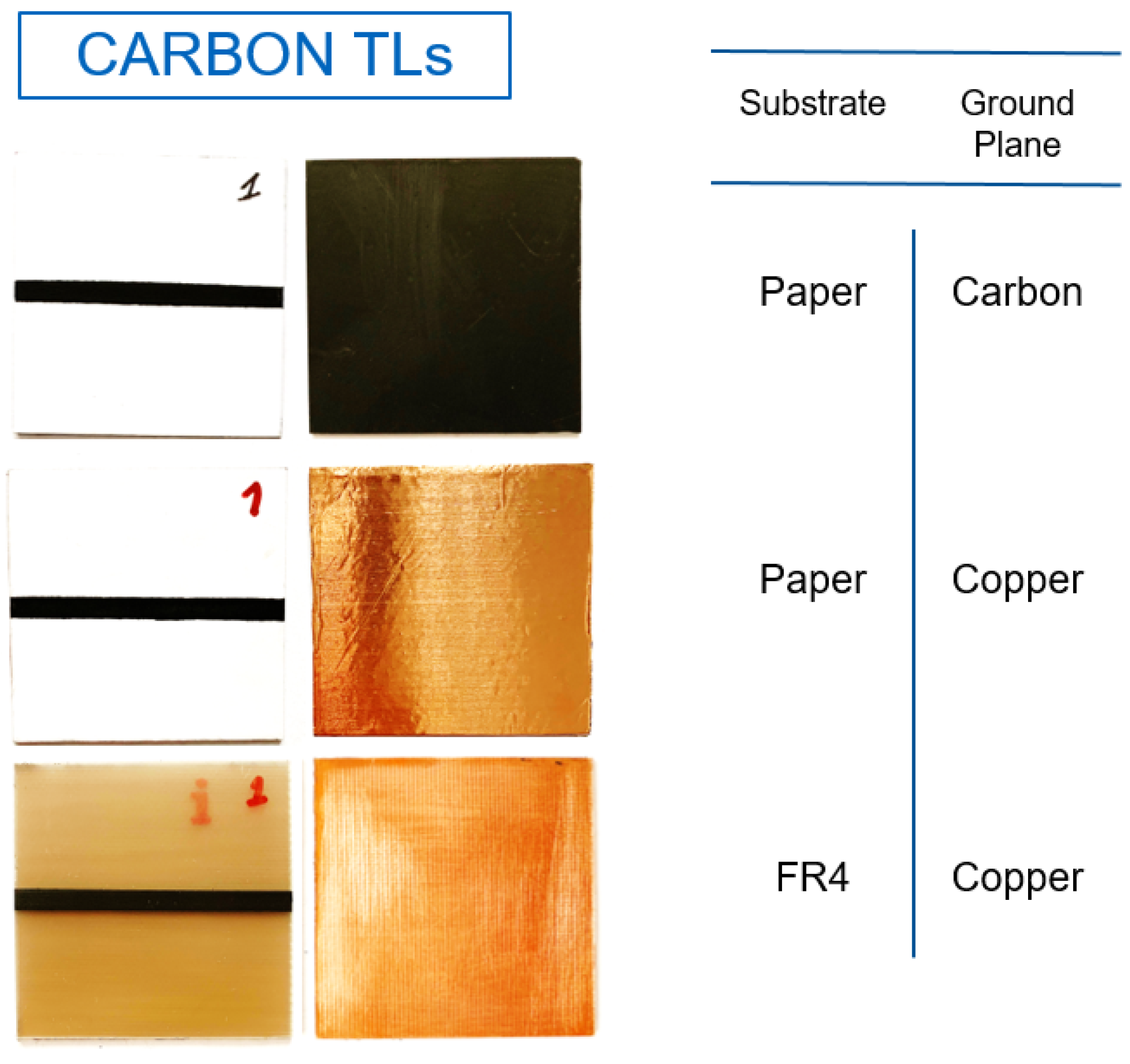
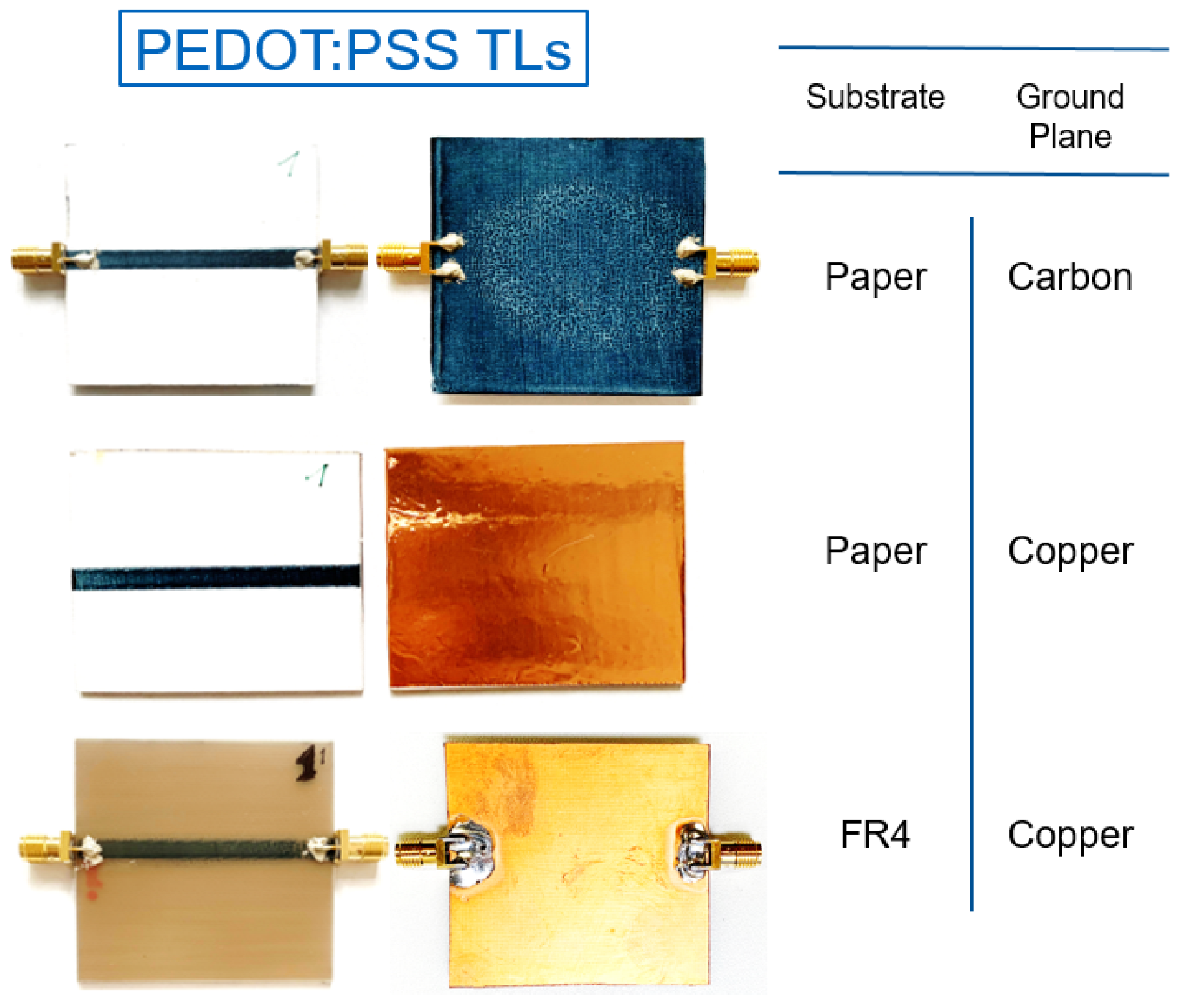
In order to check the feasibility of the organic pastes for RF signal transmission, multiple transmission lines were screen printed. For each paste, three different samples were printed: the first one is the organic sample, which is the organic pastes printed on paper substrate for both the transmission line and the ground plane. The second sample is the organic pastes printed on paper substrate but with copper ground plane (a copper tape was utilized). The last and third sample is the organic pastes printed on FR4 substrate, which has a copper ground plane. The second and the third samples were realized to compare the results with the fully organic sample, which is the goal of this work. Figure 3 and Figure 4 show the respective samples for both organic pastes.
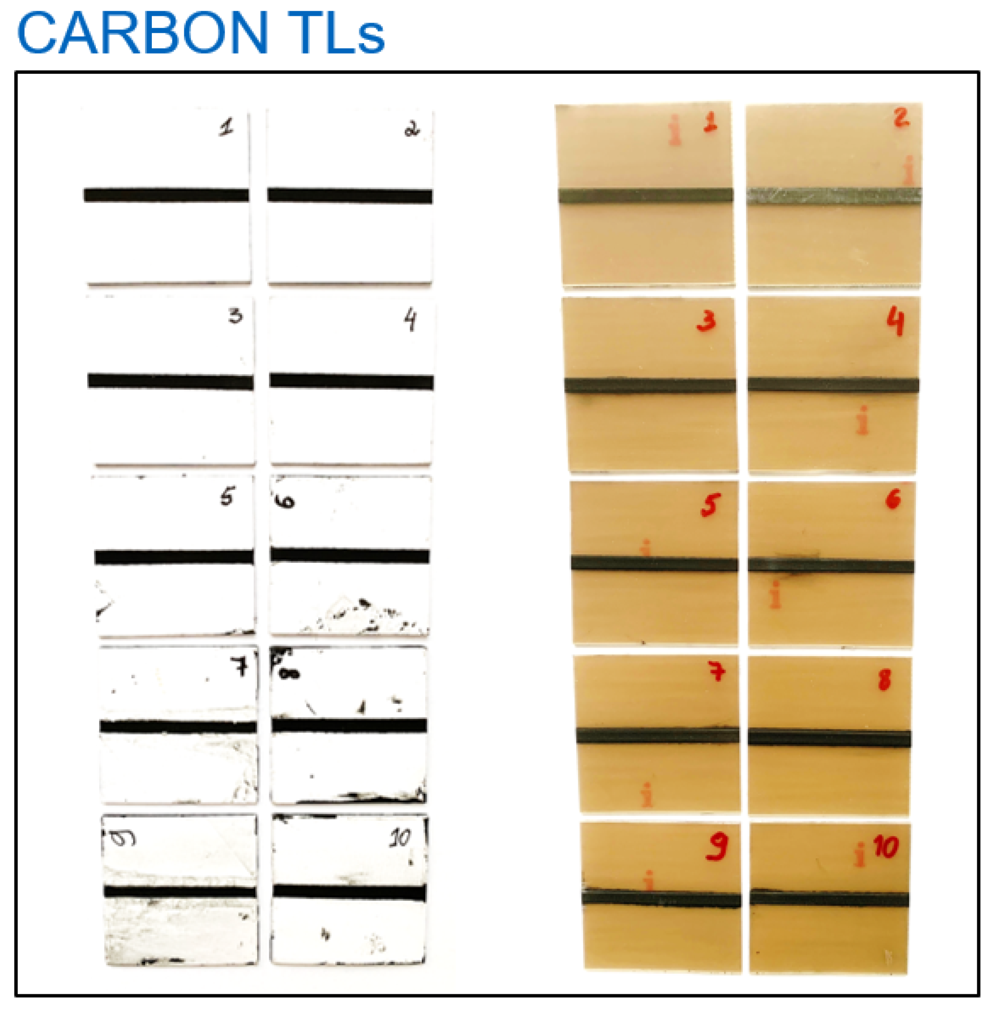
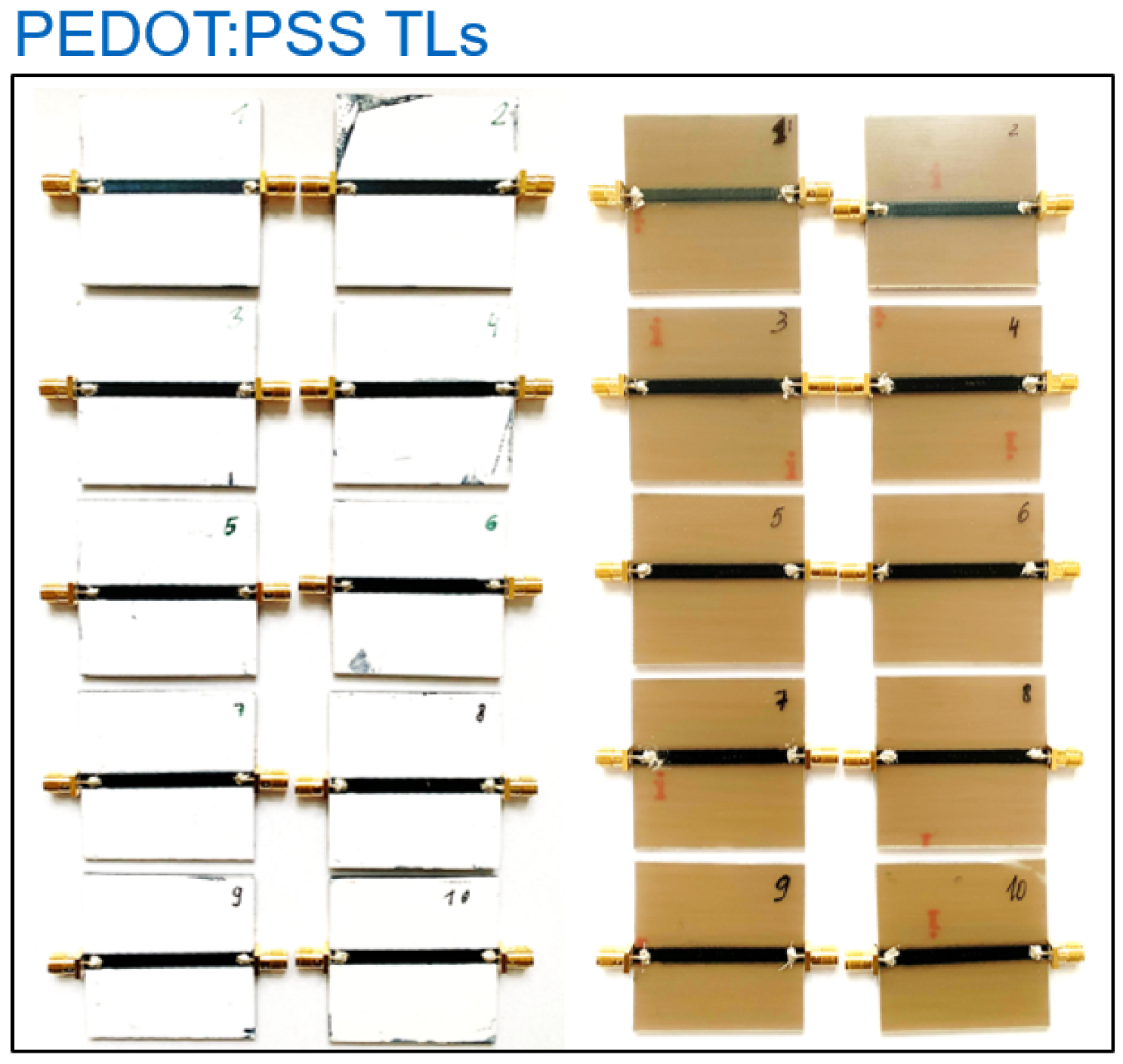
For both pastes, samples from 1 to 10 layers were printed on paper substrate and on FR4 to verify the thickness behavior and to analyze the possibility of using the materials with respect to their conductivity. The numbers of layers for the ground plane of the organic samples are the same for the transmission line and the ground plane. The samples are shown in Figure 5 and Figure 6.
The SMA connectors were attached with conductive silver epoxy from Circuit Works, so the pastes and the paper were not damaged by soldering.

5. Results

In order to evaluate the performance of the transmission lines realized with screen printing, an etched transmission line with the same design was performed with copper on FR4 as a reference for further measurements.

5.1. Reference Transmission Line

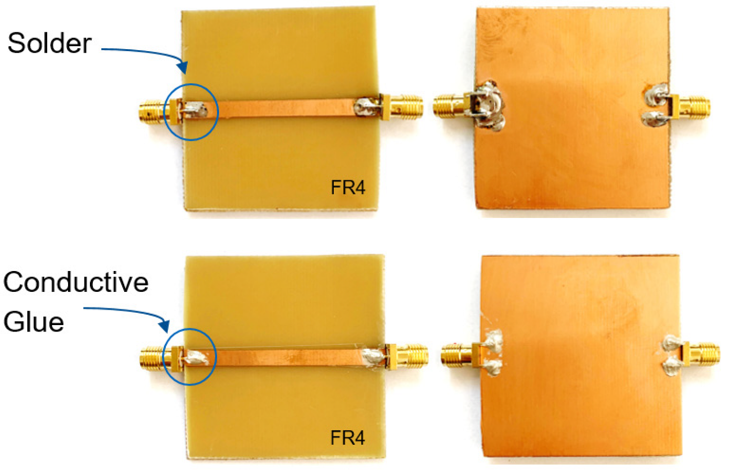
In order to have a reference sample and to check the losses from using the conductive epoxy to attach the connectors, two etched TLs samples were realized using FR4 substrate. The connectors were then attached to one sample by soldering and the other sample by gluing with the conductive epoxy, as can be seen in Figure 7.
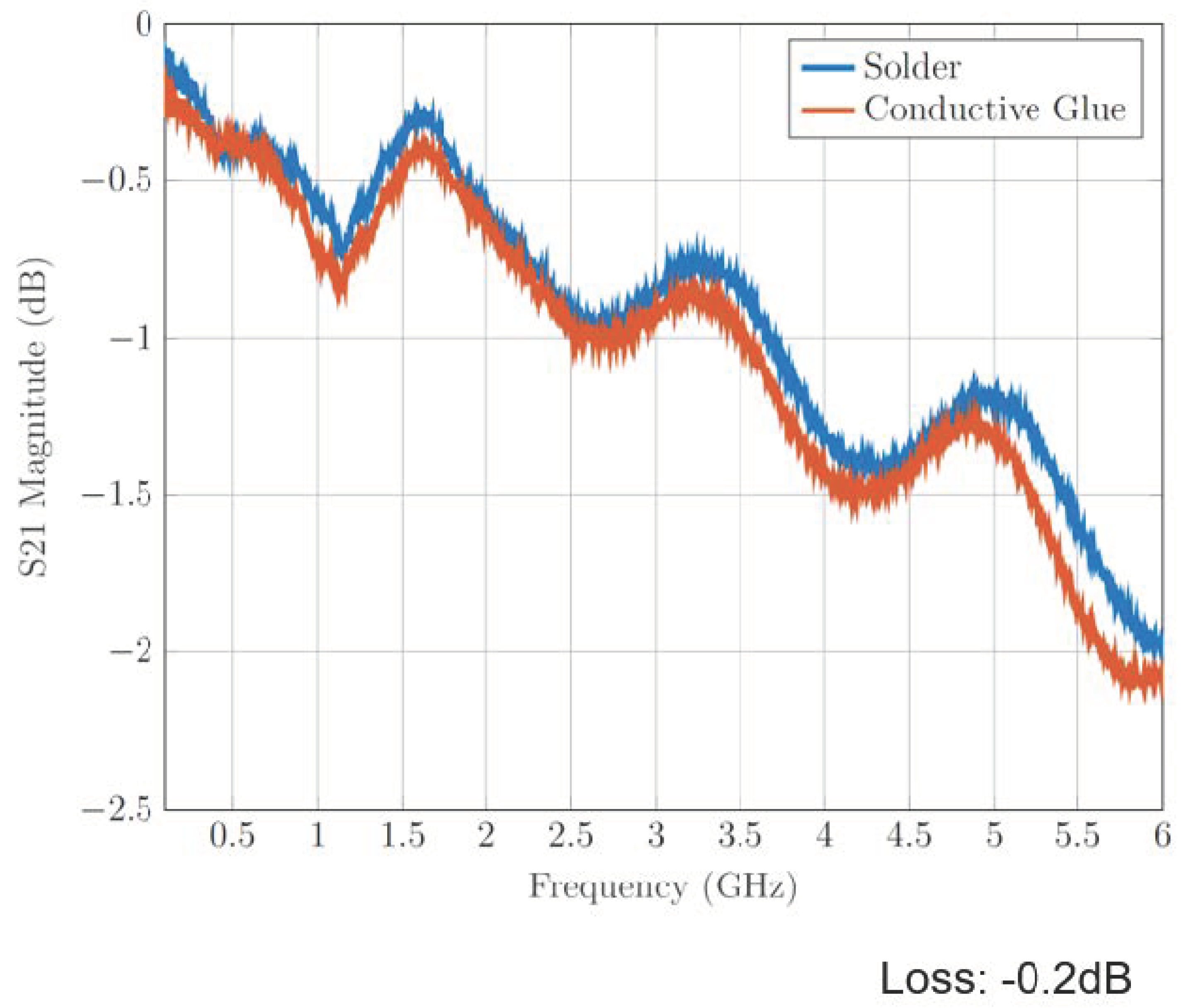
The samples were measured and the results in Figure 8 show that the losses are minimal when using the conductive epoxy, approximately −0.2 dB at 100 MHz. The wiggles are due to the impedance mismatch between the line and the connectors, but it makes no difference to the measurements.

5.2. S21 Measurements

The S21 parameter is a very important indicator of the maximum power transfer of a transmission line and it shows how much of the signal is being transmitted.
The measurements were realized with a Vector Network Analyzer and exported to MatLab to plot the results. The S21 parameter was analyzed from 100 MHz to 6 GHz.
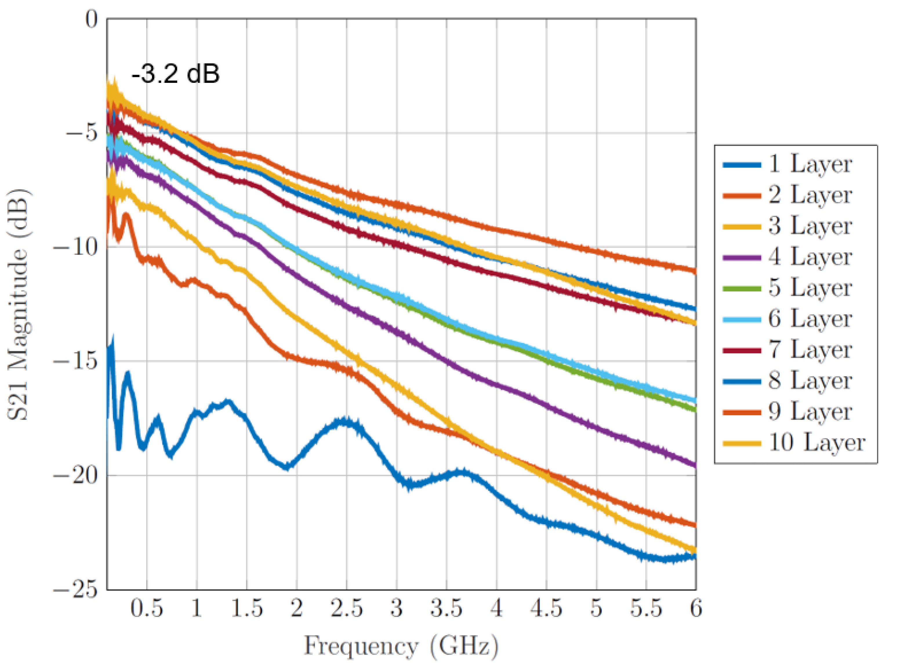
Figure 9 shows the S21 measurements of carbon on paper with a carbon ground plane. As expected, the thicker the line, the better the transmission. For the sample with 10 layers, the losses are 3.2 dB. The curve of the 10 layers performs worse than the 9 layers above 1 GHz. As the performance for the 10 layers degrades only for higher frequencies, problems with the repeatability of printing with increasing number of layers and the higher probability for process errors are the suspected cause.
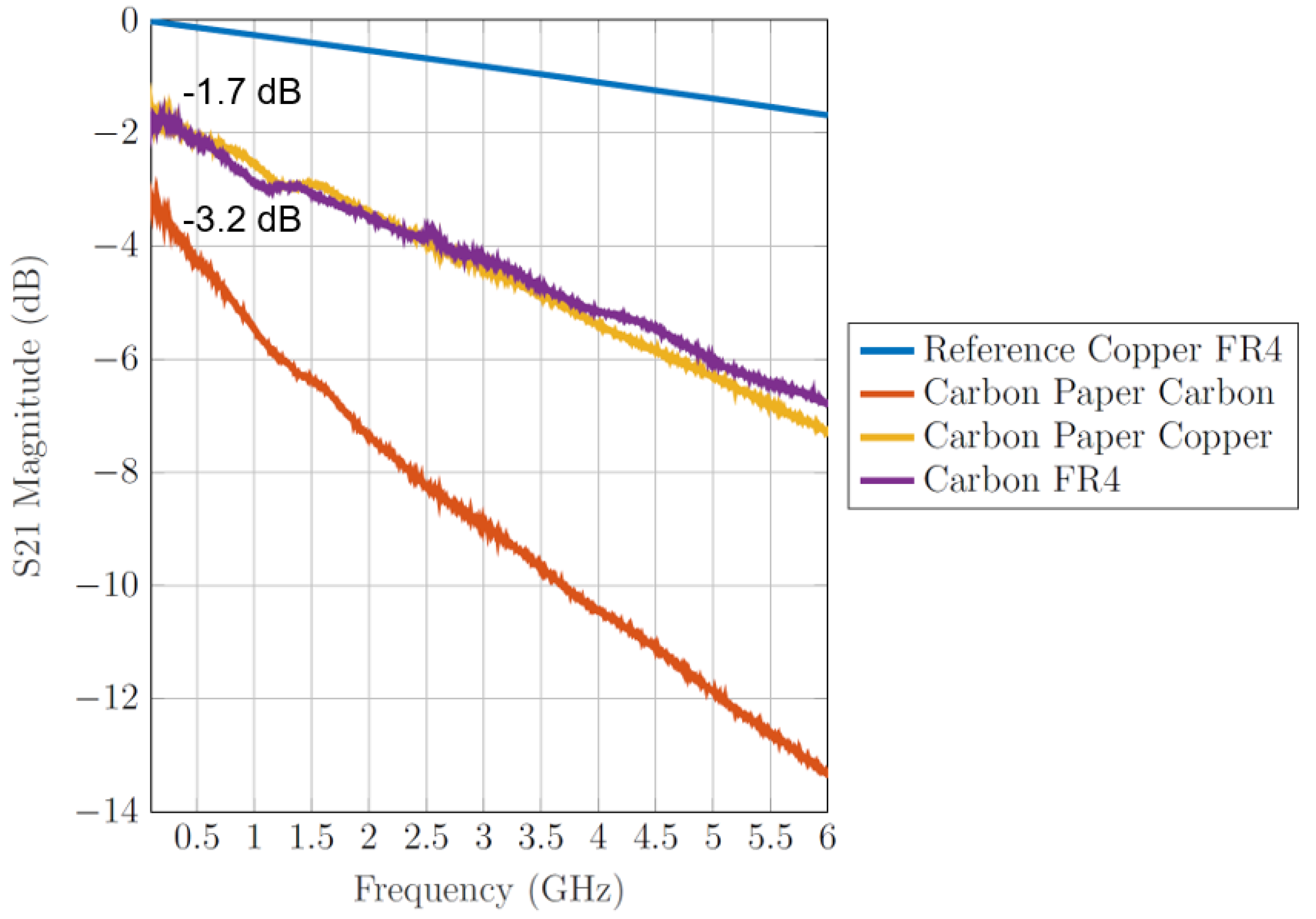
Figure 10 shows the comparison between the three carbon samples with 10 layers of carbon each, as well as the reference transmission line. As expected, the samples with copper ground plane, due to the material characteristics, on paper and on FR4 substrates have better transmission than the organic samples. The carbon and copper on paper and the carbon on FR4 samples have very similar results, −1.7 dB loss at 100 MHz. The carbon on paper with carbon ground plane has a loss of −3.2 dB, 1.5 dB worse than the other samples, but still performing reasonably for small outline printed circuits.
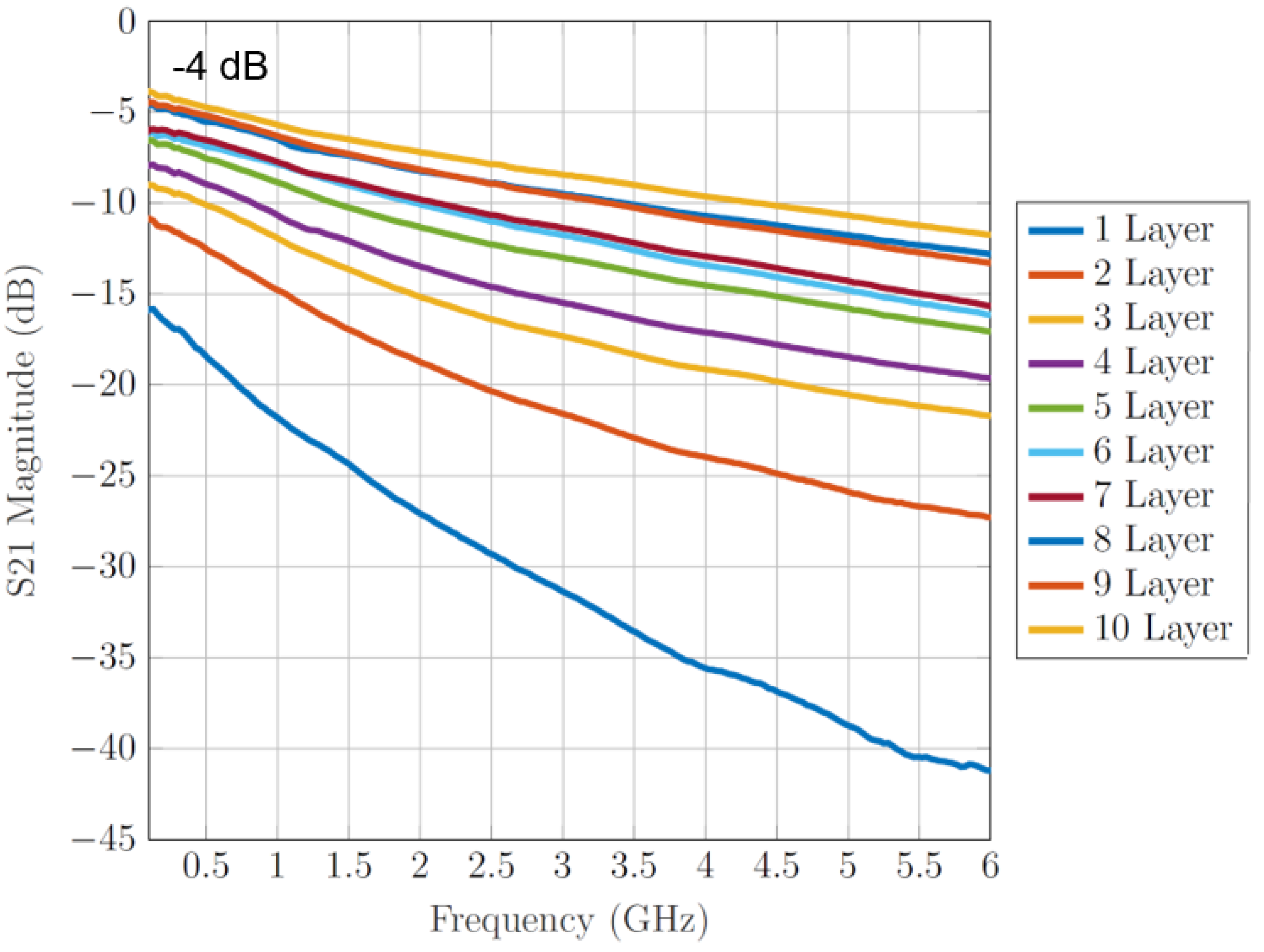
For the PEDOT:PSS paste, the measurements can be seen in Figure 11 from 1 to 10 layers’ thickness, and it shows the same behavior as the results of the carbon samples but the thickness is more consistent than the carbon samples, due to the layer’s homogeneity. The loss with the 10 layers sample is −4 dB at 100 MHz.
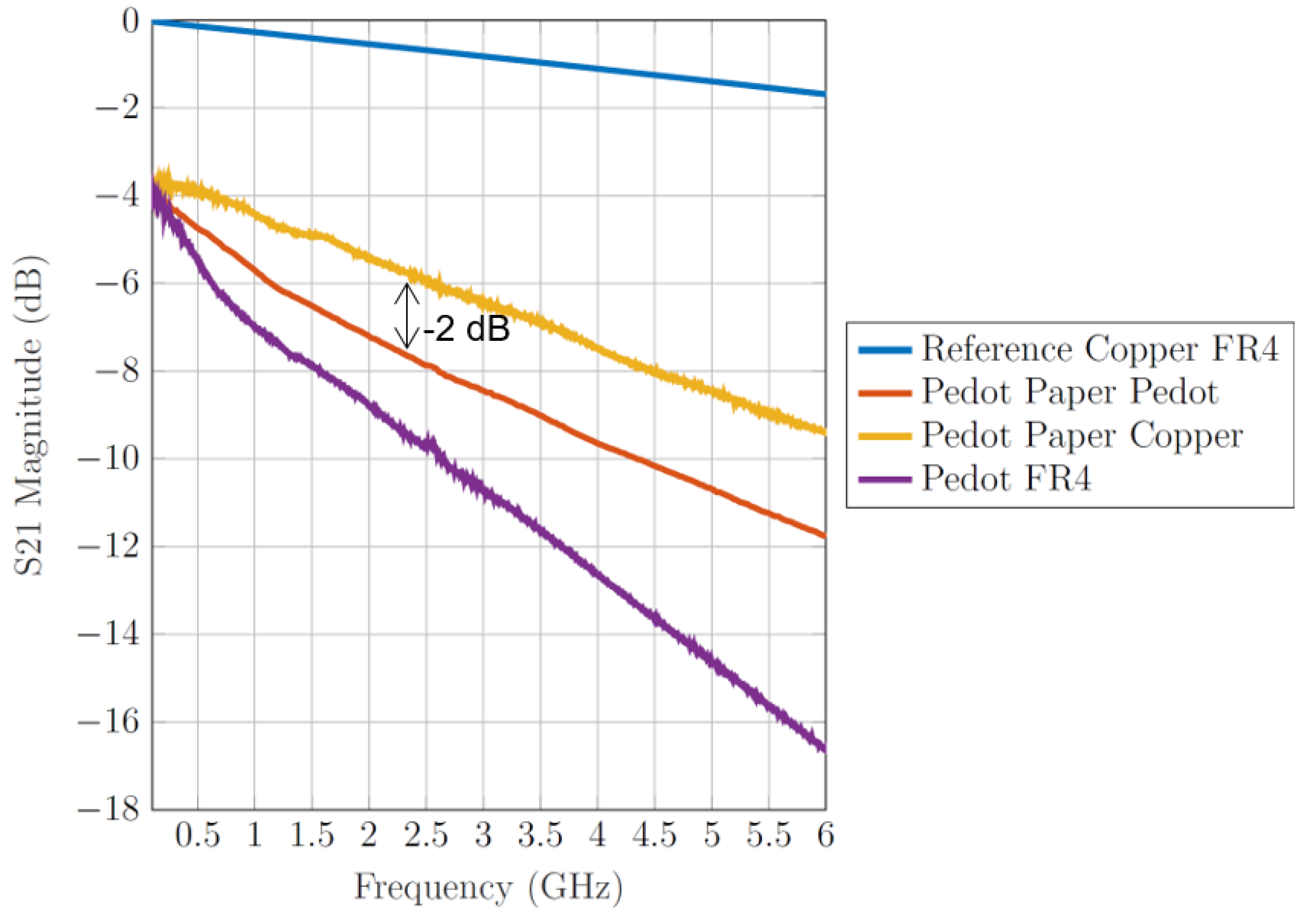
The comparison between the samples is shown in Figure 12. When one compares the organic sample with the other samples, one can observe the same behavior as for the carbon samples, except when using FR4 as a substrate, which is not the expected result. The conclusion about this behavior is that FR4 is not a suitable substrate when using the PEDOT:PSS paste. The paste does not adhere well to the FR4 surface as it is quite sleek. Perhaps with a coating on FR4 it could work better. The difference in loss is about −2 dB.
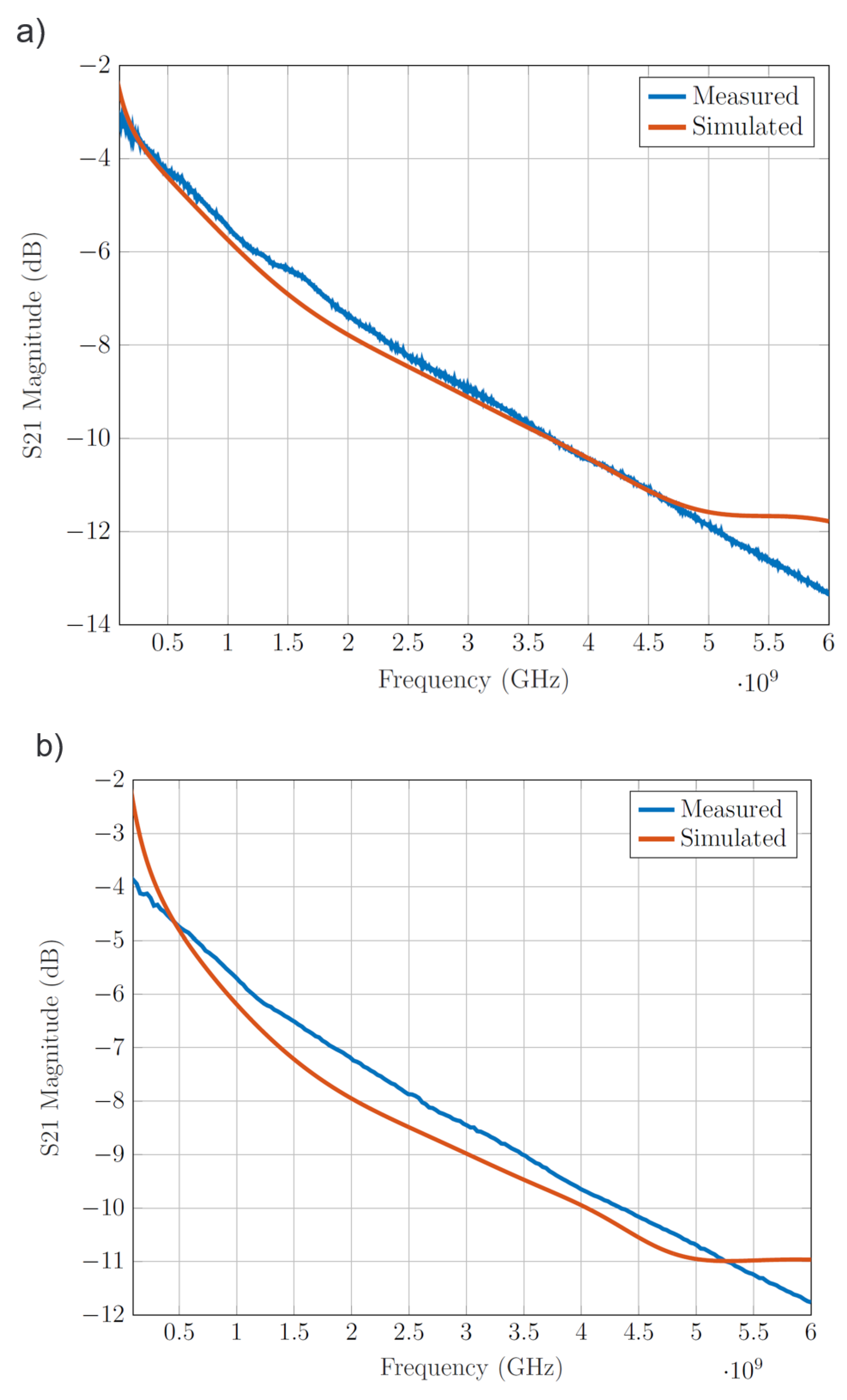
With the results from the measurements, the features from the materials were extracted and inserted in the CST Studio Suite software to simulate the transmission lines.
The simulations were realized for Carbon and PEDOT:PSS for the 10 layers’ sample, as it has the best transmission of all samples. The comparison between measurement and simulation for both samples are shown in Figure 13.
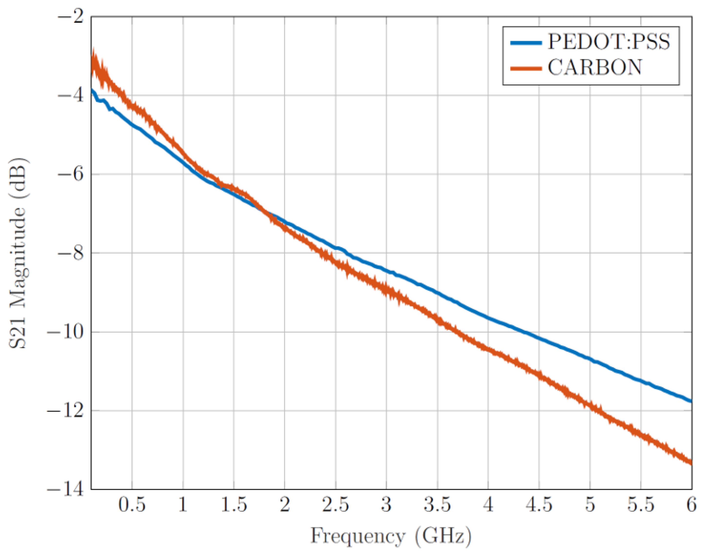
To analyze the difference between materials, a comparison between Carbon and PEDOT:PSS was plotted. Carbon shows better transmission than PEDOT:PSS, as can be seen in Figure 14.
An unusual behavior of carbon at higher frequencies can be observed, above 1.5 GHz. The reason could be due to the surface roughness, or because the last layer was unusually long or complex, and not the same as the other layers.

5.3. Material Characteristics

The measurements and the simulations allowed the possibility of estimating the features from both materials, such as thickness and conductivity from the conductors and relative permittivity from the substrates.
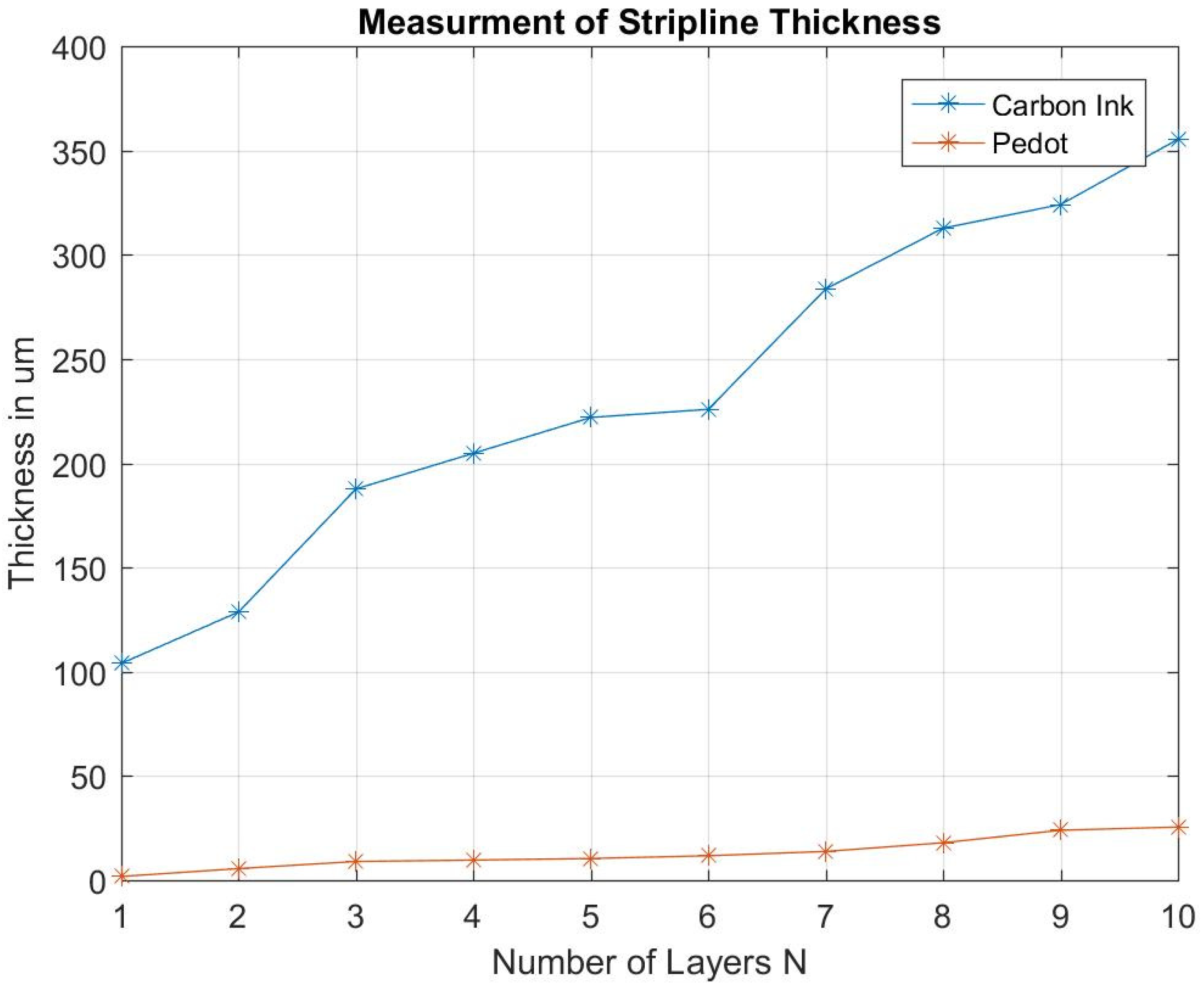
The thickness was measured with the profilometer Dektak XT from Brucker and the samples with 10 layers were 180.1 µm and 33.9 µm for carbon and PEDOT:PSS, respectively.
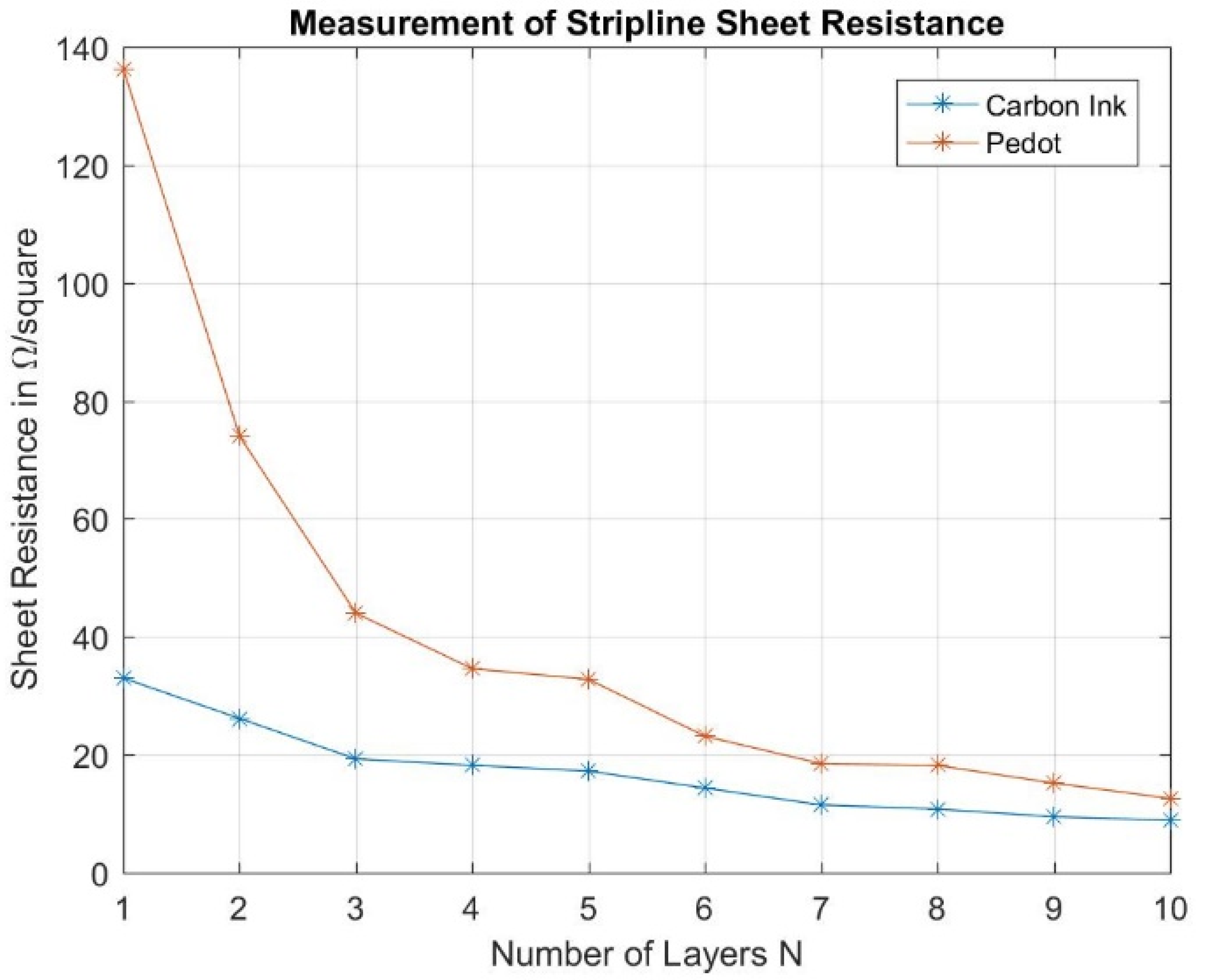
For conductivity, CST Studio Suite was used to simulate the transmission lines with specific conductivities, which were then compared to the results from the measured transmission lines. Carbon presents a conductivity of 6.65   × 10 3   S / m and PEDOT:PSS 15 × 10 3   S / m . Even though the conductivity of PEDOT:PSS is higher than carbon, the transmission of carbon is better, which is due to the fact that the carbon film is thicker, which results in a lower sheet resistance.
The relative permittivity ε r of paper is 2.9 and of FR4 is 4.7. The electrical length from the transmission lines was measured with a VNA and the ε r was calculated using the ‘line calc’ from ADS.
Figure 15 and Figure 16 show the thickness and the sheet resistance, respectively, for PEDOT:PSS and Carbon, due to the number of printed layers.

6. Applications

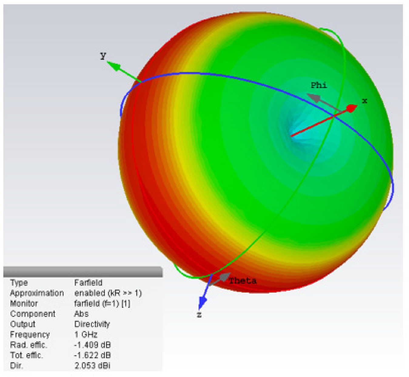
As an example of application, a dipole antenna on paper with 10 layers carbon and with 10 layers PEDOT:PSS were simulated. The simulations show good results and the efficiency for carbon is 77.2% and for PEDOT:PSS is 68.83%. The farfield 3D pattern from a dipole PEDOT:PSS antenna is shown in Figure 17.

7. Conclusions

This paper has shown the use of PEDOT:PSS and carbon-based paste on paper substrate instead of metal conductors in order to minimize the impact of the traditional manufacturing techniques in RF circuit design. Transmission lines were printed in order to investigate the feasibility of the two pastes for RF signal transmission. The approach is based on the screen printing of conductive pastes on organic substrates and the results show through S 21 parameter measurements that both pastes are feasible for RF signal transmission, even though carbon shows better transmission than PEDOT:PSS due to its thickness. The features of the materials such as conductivity, thickness and relative permittivity were presented as well. This approach enables the manufacturing process in RF circuit design to become more environmentally friendly and it results in many possibilities for application in antenna design, wearable electronics, RFID-based sensors, biocompatible and biodegradable sensors. It is not suitable, though, for all general RF applications.

Author Contributions

Conceptualization, B.C. and P.E.; methodology, B.C.; software, P.E.; validation, B.C. and M.H.; formal analysis, B.C.; investigation, B.C.; resources, B.C.; data curation, M.H.; writing—original draft preparation, B.C.; writing—review and editing, B.C.; visualization, B.C.; supervision, E.B.; project administration, E.B.; funding acquisition, E.B. All authors have read and agreed to the published version of the manuscript.

Funding

This research received no external funding.

Conflicts of Interest

The authors declare no conflict of interest.

References

  1. Cuerchouche, K.; Herth, E.; Calvet, L.; Roland, N.; Loyez, C. Conductive Polymer Based Antenna for Wireless Green Sensors Application; Elsevier: Amsterdam, The Netherlands, 2017; Volume 182, pp. 46–52. [Google Scholar] [CrossRef]
  2. Li, Z.; Sinha, S.K.; Treich, G.M.; Wang, Y.; Yang, Q.; Deshmukh, A.A.; Sotzing, G.A.; Cao, Y. All-Organic Flexible Fabric Antenna for Weareble Electronics. J. Mater. Chem. C 2020, 8, 5662–5667. [Google Scholar] [CrossRef]
  3. Mehdipour, A.; Sebak, A.R.; Trueman, C.W.; Rosca, I.D.; Hoa, S.V. Conductive Carbon Fiber Composite Materials for Antenna and Microwave Applications. In Proceedings of the 2012 29th National Radio Science Conference (NRSC), Cairo, Egypt, 10–12 April 2012; pp. 1–8. [Google Scholar] [CrossRef]
  4. Zhang, X.; Cui, Y.; Lv, Z.; Li, M.; Ma, S.; Cui, Z.; Kong, Q. Carbon Nanotubes, Carbon Black and Graphite Powder Based Paste Electrodes. Int. J. Electrochem. Sci. 2011, 6, 6063–6073. [Google Scholar]
  5. Suganuma, K. Introduction to Printed Electronics; Springer Science & Business Media: Berlin/Heidelberg, Germany, 2017; Volume 74. [Google Scholar]
  6. Zheng, C. Printed Electronics: Manufacturing Technologies and Applications; John Wiley & Sons Singapore Pte. Ltd.: Singapore, 2014. [Google Scholar]
  7. Nisato, G.; Lupo, D.; Ganz, S. Organic and Printed Electronics: Fundamentals and Applications; CRC Press: Boca Raton, FL, USA, 2016. [Google Scholar]
  8. Pardo, D.A.; Jabbour, G.E.; Peyghambarian, N. Application of Screen Printing in the Fabrication of Organic Light-Emitting Devices. Adv. Mater. 2000, 12, 1249–1252. [Google Scholar] [CrossRef]
  9. Albrecht, A. Printed Sensors for the Internet of Things; Technical University of Munich: Munich, Germany, 2018. [Google Scholar]
  10. Khan, S.; Lorenzelli, L.; Dahiya, R.S. Screen printed flexible pressure sensors skin. In Proceedings of the 25th Annual SEMI Advanced Semiconductor Manufacturing Conference (ASMC), Saratoga Springs, NY, USA, 19–21 May 2014; pp. 219–224. [Google Scholar]
  11. Lipomi, D.; Lee, J.; Vosgueritchian, M.; Tee, B.; Bolander, J.; Bao, Z. Electronic properties of transparent conductive films of PEDOT:PSS on strechable substrates. Chem. Mater. 2012, 24, 373–382. [Google Scholar] [CrossRef]
  12. Datasheet Orgacon. Available online: https://kayakuam.com/wp-content/uploads/2020/03/Technical-Data-Sheet-ORGACON-EL-P-April-22-2021.pdf (accessed on 1 January 2020).
  13. Datasheet Microchem. Available online: https://kayakuam.com/wp-content/uploads/2020/03/C-200-Carbon-Ink.pdf (accessed on 1 January 2020).
  14. Tobjörk, D.; Österbacka, R. Paper electronics. Adv. Mater. 2011, 23, 1935–1961. [Google Scholar] [CrossRef] [PubMed]
  15. Roselli, L. Green RFID Systems; Cambridge University Press: Cambridge, UK, 2014. [Google Scholar] [CrossRef]
  16. Khaleel, H. Innovation in Wearable and Flexible Antennas; WIT Press: Boston, MA, USA, 2015. [Google Scholar]
  17. Steer, M. Microwave and RF Design: Transmission Lines, 3rd ed.; NC State University: Raleigh, NC, USA, 2019; Volume 2. [Google Scholar] [CrossRef]
  18. Sefar, Product Information. Guide for Precision Electronic Screens; Sefar, Product Information: Buffalo, NY, USA, 2015. [Google Scholar]
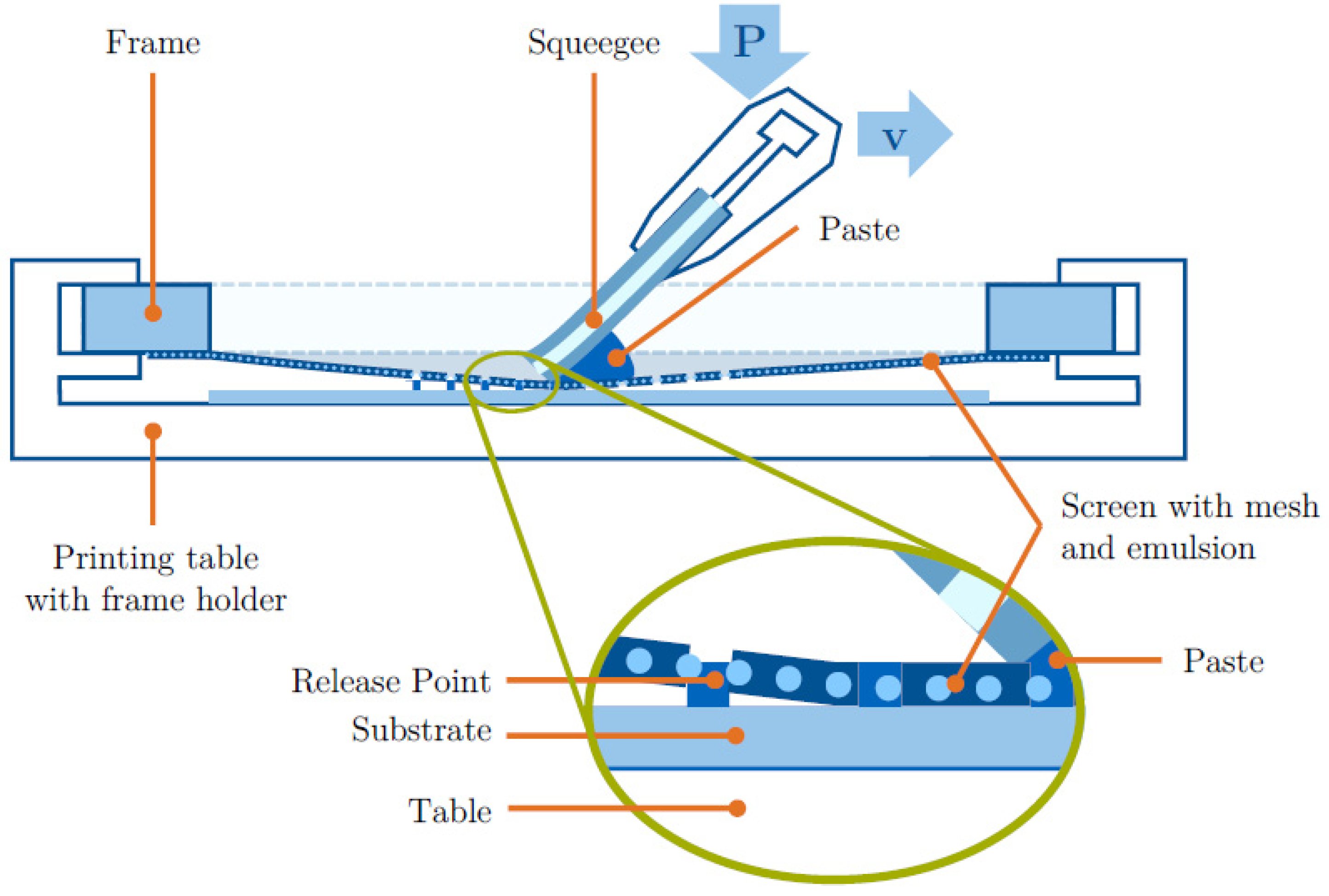
Figure 1. Screen printing technique. Reprinted with permission from Ref. [9].
Electronicmat 03 00023 g001
Figure 2. Manufacturing process of the Carbon ground planes using the high precision printer Nino.
Electronicmat 03 00023 g002
Figure 3. Carbon transmission lines on paper substrate with carbon ground plane, copper ground plane and on FR4 substrate with copper ground plane.
Electronicmat 03 00023 g003
Figure 4. PEDOT:PSS transmission lines on paper substrate with PEDOT:PSS ground plane, copper ground plane and on FR4 substrate with copper ground plane.
Electronicmat 03 00023 g004
Figure 5. Samples from 1 to 10 layers of carbon on paper and FR4 substrates, respectively.
Electronicmat 03 00023 g005
Figure 6. Samples from 1 to 10 layers of PEDOT:PSS on FR4 and paper substrates, respectively.
Electronicmat 03 00023 g006
Figure 7. SMA connectors attached to the samples by soldering and by gluing, respectively.
Electronicmat 03 00023 g007
Figure 8. Loss due to the use of conductive epoxy when comparing with solder.
Electronicmat 03 00023 g008
Figure 9. S21 parameter of carbon sample with carbon ground plane from 1 to 10 layers.
Electronicmat 03 00023 g009
Figure 10. Transmission comparison between the 10 layers carbon samples and the reference transmission line.
Electronicmat 03 00023 g010
Figure 11. S21 parameter of PEDOT:PSS sample with PEDOT:PSS ground plane from 1 to 10 layers.
Electronicmat 03 00023 g011
Figure 12. Transmission comparison between the 10 layers PEDOT:PSS samples and the reference transmission line.
Electronicmat 03 00023 g012
Figure 13. S21 parameter simulated versus measured (a) for carbon on paper TL and (b) for PEDOT:PSS on paper TL.
Electronicmat 03 00023 g013
Figure 14. S21 parameter comparison between Carbon and PEDOT:PSS on paper substrate for 10 layers.
Electronicmat 03 00023 g014
Figure 15. Measurement of the transmission line for the thickness of PEDOT:PSS and Carbon versus number of layers.
Electronicmat 03 00023 g015
Figure 16. Measurement of the transmission line for the sheet resistance of PEDOT:PSS and Carbon versus number of layers.
Electronicmat 03 00023 g016
Figure 17. Fairfield 3D pattern of a PEDOT:PSS dipole antenna.
Electronicmat 03 00023 g017
Publisher’s Note: MDPI stays neutral with regard to jurisdictional claims in published maps and institutional affiliations.