Article

Theoretical Prediction of Heterogeneous Integration of Dissimilar Semiconductor with Various Ultra-Thin Oxides and 2D Materials

Department of Materials Design and Innovation, University at Buffalo, The State University of New York (SUNY), Buffalo, NY 14260, USA
*
Author to whom correspondence should be addressed.
Electron. Mater. 2021, 2(4), 495-503; https://doi.org/10.3390/electronicmat2040034
Submission received: 3 September 2021 / Revised: 23 September 2021 / Accepted: 6 October 2021 / Published: 11 October 2021
(This article belongs to the Special Issue Feature Papers of Electronic Materials)

Abstract

:
In this paper, we build a numerical p-n Si/GaAs heterojunction model using quantum-mechanical tunneling theory with various quantum tunneling interfacial materials including two-dimensional (2D) materials such as hexagonal boron nitride (h-BN) and graphene, and ALD-enabled oxide materials such as HfO2, Al2O3, and SiO2. Their tunneling efficiencies and tunneling currents with different thicknesses were systematically calculated and compared. Multiphysics modeling was used with the aforementioned tunneling interfacial materials to analyze changes in the strain under different temperature conditions. Considering the transport properties and thermal-induced strain analysis, Al2O3, among three oxide materials, and graphene in 2D materials are favorable material choices that offer the highest heterojunction quality. Overall, our results offer a viable route in guiding the selection of quantum tunneling materials for a myriad of possible combinations of new heterostructures that can be obtained with an ultra-thin tunneling intermediate layer.

1. Introduction

Semiconductor heterojunctions have long been considered one of the most important building blocks of the semiconductor industry. They have led to various practical electronic and optoelectronic applications such as lighting devices (light-emitting devices and lasers), sensors, transistors, and photovoltaics [1,2,3,4,5,6,7]. All of these applications have used lattice-matched (or slightly mismatched) semiconductor systems such as Si/SiGe, GaAs/AlGaAs, or GaN/AlGaN [8,9,10]. While a tremendous amount of effort has been devoted to these systems to create high-quality heterojunctions, these heterogeneous integrations must be made within a very strict lattice match rule [11,12,13,14,15]. To overcome this limitation and restriction, namely to integrate dissimilar/lattice mismatched semiconductors, various novel approaches have been proposed. In the early days, advanced wafer bonding techniques, such as surface-activated bonding (SAB), were introduced and applied to demonstrate various Si-to-III-V solar cells and transistors [16,17]. However, this method has several restrictions in that the source materials must exist in the form of the wafer, and the defect formation is due to different lattice parameters between to-be-bonded semiconductors. Recently, another heterogeneous integration method has been reported by introducing an ultra-thin intermediate layer between two to-be-bonded semiconductors: the Ultra-thin Tunneling intermediate layer (UT) method, which uses a sub-nanometer thick quantum tunneling layer that is prepared by atomic layered deposition (ALD) [4,18,19]. The UT-based heterogeneous integration method was developed to realize a high-quality integration among semiconductor membranes. This integration process involves (1) the creation of semiconductor nanomembranes; (2) the deposition (or formation) of the ultra-thin intermediate layer; and (3) the micro-transfer printing technique, which allows us to manipulate semiconductor nanomembranes. To create the heterostructure, one or more semiconductor nanomembranes need to be transfer-printed onto another semiconductor substrate. The core of this idea is to passivate the surface prior to bonding two semiconductors using an ultra-thin layer to prevent its surface from growing an unwanted native oxide layer or dangling bonds. At the same time, the thin tunneling layer facilitates the carrier transport across the interfacial layer; thus, a high-quality heterostructure that has a substantially lower degree of interface defect density can be achieved. In this way, a high-quality arbitrary heterogeneous integration between two dissimilar single-crystalline semiconductors can be realized regardless of their crystal orientations, thermal expansion, and lattice constants. To date, most experimentally demonstrated heterostructures use aluminum oxide, and other quantum tunneling interfacial materials have not yet been explored.
In this paper, we build a numerical p-n Si/GaAs heterojunction model using quantum-mechanical tunneling theory with various quantum tunneling interfacial materials including two-dimensional (2D) materials such as hexagonal boron nitride (h-BN) and graphene, and ALD-enabled oxide materials such as HfO2, Al2O3, and SiO2. Their tunneling efficiencies and tunneling current with different thicknesses were then systematically calculated and compared. Finally, multiphysics modeling was performed with the aforementioned tunneling interfacial materials to analyze the changes in strain under different temperature conditions. Overall, our results offer a viable route in guiding the selection of quantum tunneling materials for a myriad of possible combinations of new heterostructures that can be obtained via the UT method.

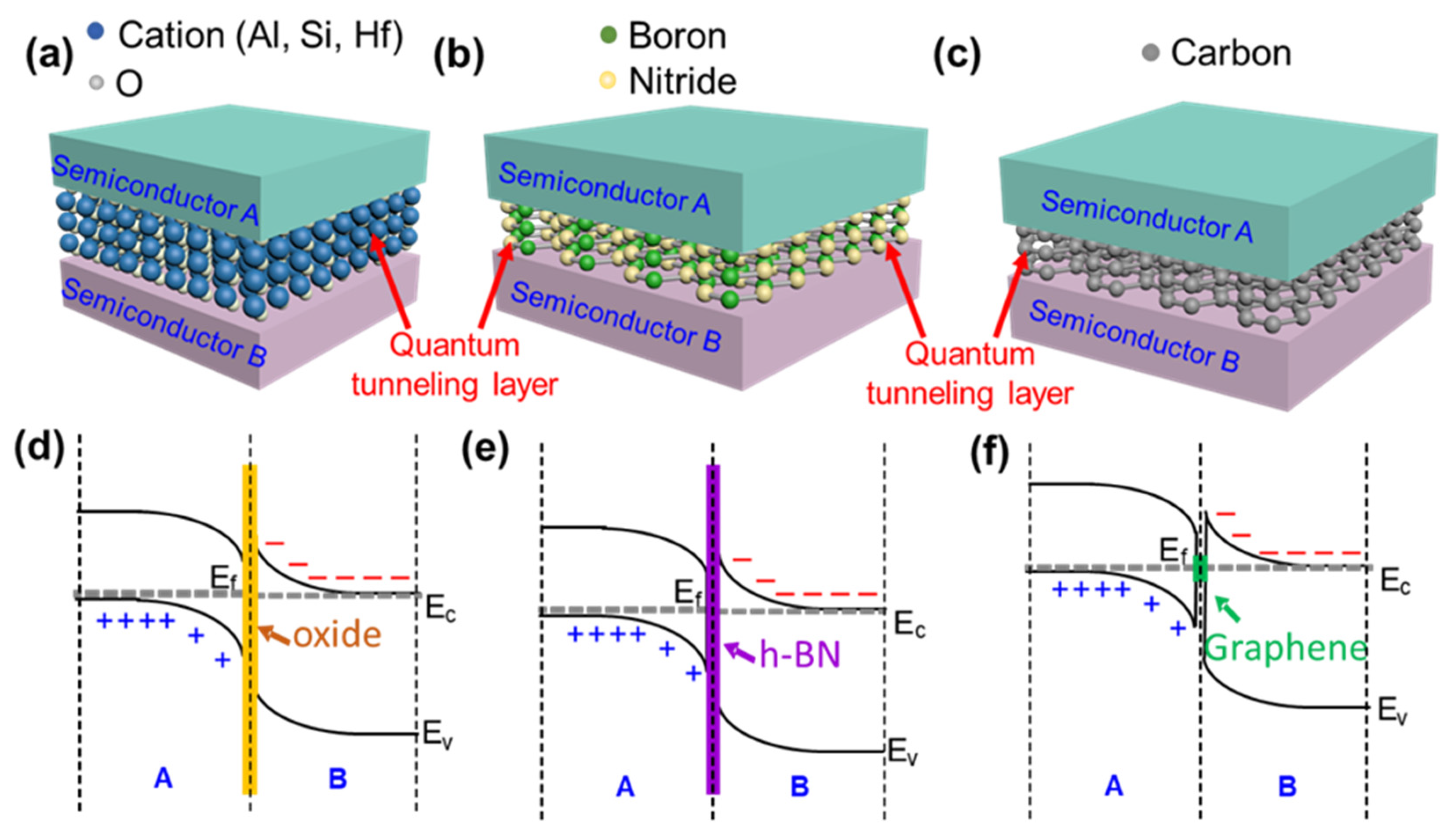
2. Materials and Methods

Figure 1a–c shows a schematic illustration of the heterogeneous integration of two dissimilar semiconductors sandwiched between ultra-thin oxide and 2D materials. Figure 1 shows that semiconductors A and B are different lattice-mismatched materials with an ultra-thin quantum tunneling layer. In most cases, oxides and h-BN create tunneling barriers, but the graphene layer forms a quantum well, leading to different band offsets. In this calculation, we employed p-type Si and n-type GaAs; each quantum tunneling layer was seen among h-BN, graphene HfO2, Al2O3, and SiO2 with different thicknesses from 0.3 nm to 1.3 nm. It should be noted that direct tunneling is used for carrier transport calculation in this study because this study primarily focuses on an ultra-thin oxide and a 2D material’s interface (<2 nm) [20,21]. A continuous wave function was employed to investigate the tunneling probability (T) of carriers (electrons and holes) across the heterointerface. A wave function incident at the tunneling barrier is a part of the wave transmitted through the barrier; another part of the wave is thus reflected back. Hence, the transmitted wave is considered a tunneling carrier. To explain this phenomenon, we considered the one-dimensional Schrödinger wave equation, as follows. A detailed solution of Equation (1) for different conditions such as before the tunneling barrier (incident wave) and after the tunneling barrier (transmitted wave) was calculated.
( 2 2 m * Δ 2 + V ( x ) ) Ψ ( x ) = E Ψ ( x )
Considering all boundary conditions, the tunneling probability is derived as the modulus squared of the transmitted wave ratio to the incident wave function. A detailed derivation of Equation (1) can be found in the Supplementary Materials.
T = 4 E ( V 0 E ) V 0 2 s i n h 2 ( k 2 a ) + 4 E ( V 0 E )  
where E is the potential energy of the carrier (electron or hole), V0 is the potential barrier height (conduction or valance band offset), k 2 is related to effective mass, and a is the thickness of the tunneling layer (oxide or 2D material interface). To simplify the tunneling probability across two different semiconductors, the semiconductor A-tunneling layer-semiconductor B structure (Figure 1) was divided into two sections: the semiconductor A-to-tunneling layer and the semiconductor B-to-tunneling layer. We calculated ten separated tunneling probability calculations because five different quantum tunneling materials were used: the tunneling probability of electrons in the HfO2/n-GaAs, Al2O3/n-GaAs, SiO2/n-GaAs, graphene/n-GaAs, and h-BN/n-GaAs interfaces as well as the tunneling probability of holes in the HfO2/p-Si, Al2O3/p-Si, SiO2/p-Si graphene/p-Si, and h-BN/p-Si interfaces. Both used Equation (2). Figure S1 in the Supplementary Materials represents band diagrams of these structures with different oxide tunneling layers and their barrier potential for electrons and holes.

3. Results

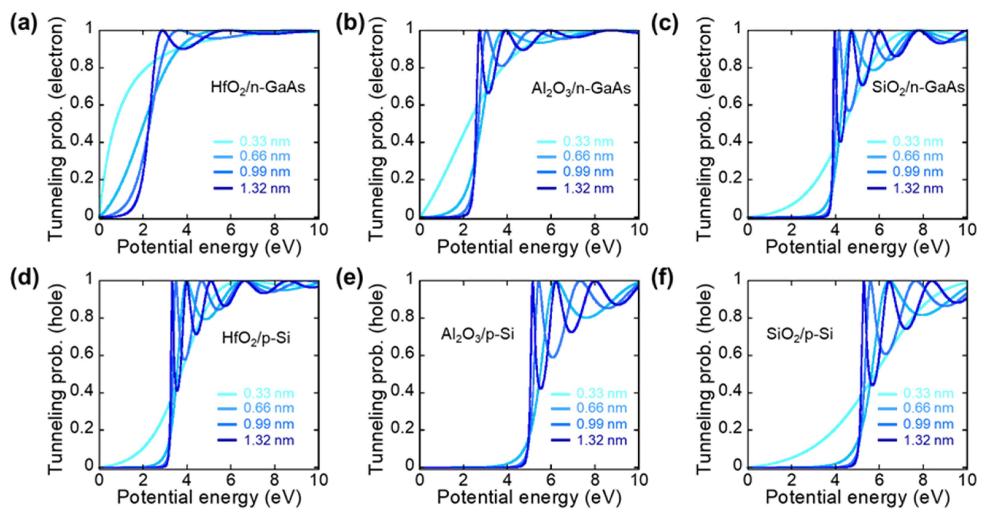
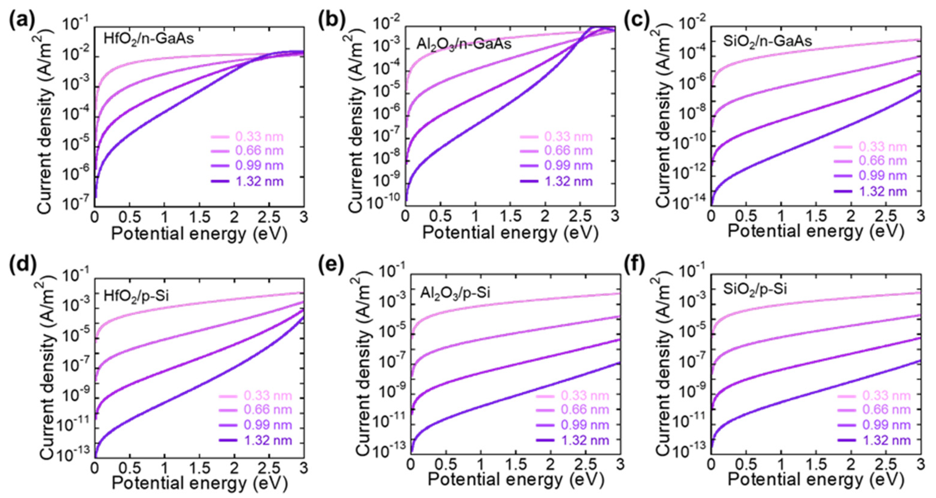
3.1. Tunneling Probability and Current Density with Ultra-Thin Oxide Intermediate Layers

Figure 2a–c shows the tunneling probability of electrons at the n-GaAs/oxide quantum tunneling layer interface. The oxide thickness increased by 0.33 nm, 0.66 nm, 0.99 nm, and 1.32 nm. Interestingly, the effective mass for the electron and barrier height played a crucial role in determining the tunneling probability. HfO2 has an electron effective mass of 0.13 m0, whereas Al2O3 and SiO2 have electron effective masses of 0.32 mo and 0.5 mo, respectively. The barrier height (ΦB) of HfO2B = 1.9 eV) is lower than those of Al2O3B = 2.33 eV) and SiO2B = 3.7 eV). Hence, a lighter electron effective mass leads to a lower barrier height and thus a higher tunneling probability. In this particular example (Si/GaAs p-n junction), it is clear that the HfO2 tunneling material is more efficient than the Al2O3- and SiO2-based tunneling layer. In addition, tunneling in quantum mechanics occurs frequently and thus leads to increased carrier transport across the heterointerface when the potential energy (E) is smaller than the barrier height [22,23]. Figure 2 shows that, when the thickness of the oxide quantum tunneling layer increased from 0.33 nm to the 1.3 nm, the tunneling probability of an electron also decreased at E < V cases [24]. When the potential energy (E) was higher than the barrier height (V), the electron can roll over the barrier and thus pass the barrier, with the classical theory dominating. However, the energy quantization effect dominates when the oxide thickness becomes thinner from 1.3 nm to 0.33 nm; thus, there is also a probability of electron tunneling via the E > V condition upon quantum tunneling. Quantum scattering theory describes the energy quantization effect such as the quantum well structure [25]. Electrons can pass through the barrier when the energy of an electron is greater than 1.9 eV (Figure 2a). As the thickness of HfO2 becomes thicker, more discrete energy levels (resonance peak) appear and suddenly cause a spike in the tunneling probability close to unity. The effective mass of the electron defines the number of resonant peaks; in other words, a higher effective mass causes more resonant peaks to appear. For example, one resonant peak appears when the Al2O3 thickness is 0.66 nm (Figure 2b), but two and three resonant peaks appear when the Al2O3 thicknesses are 0.99 nm and 1.3 nm, respectively. In addition, the SiO2 case shows stronger oscillations in resonant peaks due to a heavier electron effective mass (0.5 m0) (Figure 2c). Interestingly, the resonant peak becomes wider when the potential energy exceeds their corresponding barrier height (for example, >4.1 eV for SiO2 in Figure 2c). This can be explained by both the tunneling and overflow of the barrier at the same time. Figure 2d–f presents the tunneling probability of holes at the p-Si/oxide quantum tunneling layer interface. A higher effective hole mass in HfO2 (0.58 m0) leads to more resonant peaks than Al2O3- and SiO2-based structures. However, HfO2 shows a nearly 50% higher tunneling probability than Al2O3 and SiO2 due to the lower barrier height (3.1 eV) relative to Al2O3 and SiO2. The transport mechanism of the carriers has an exponential relationship with the thickness of the tunneling barrier [26]. As shown in the previous section, the tunneling probability across the barrier is reduced with increased tunneling layer thickness. Based on these relationships, we calculated the current density across the tunneling layer using different oxides at different thicknesses to investigate the carrier transport mechanism. The current density was calculated from J = q n V R T ( E ) , where “n” is the carrier density, T(E) is the tunneling probability, and V R is the Richardson velocity for the electron and the hole. V R was achieved from k T / 2 π m * , where k is the Boltzmann constant, T is room temperature, and m * is the effective mass of electrons and holes. Figure 3a–c presents the electron current density at HfO2/n-GaAs, Al2O3/n-GaAs, and SiO2/n-GaAs with different oxide thicknesses, respectively. In general, the calculated current density increases as the tunneling layer becomes thinner from 1.32 nm to 0.33 nm for all three oxide cases. The calculated current density for both Si and GaAs with the HfO2 tunneling layer was substantially higher (at least one order of magnitude higher) than the same structures with a Al2O3 and SiO2 tunneling layer. Figure 3d–f presents the hole current density at HfO2/p-Si, Al2O3/p-Si, and SiO2/p-Si with different oxide thicknesses, respectively, which show the increasing trend in the hole current density as the oxide layer becomes thinner. From this result, we conclude that the ideal oxide tunneling material should have a lower band offset (barrier height) and lighter effective mass to both semiconductors A and B. In addition to these parameters, several practical aspects such as thin-film coverage in a nanoscale thickness, surface passivation capability, and controllability of native oxide removal can also affect the tunneling probability across the interface.

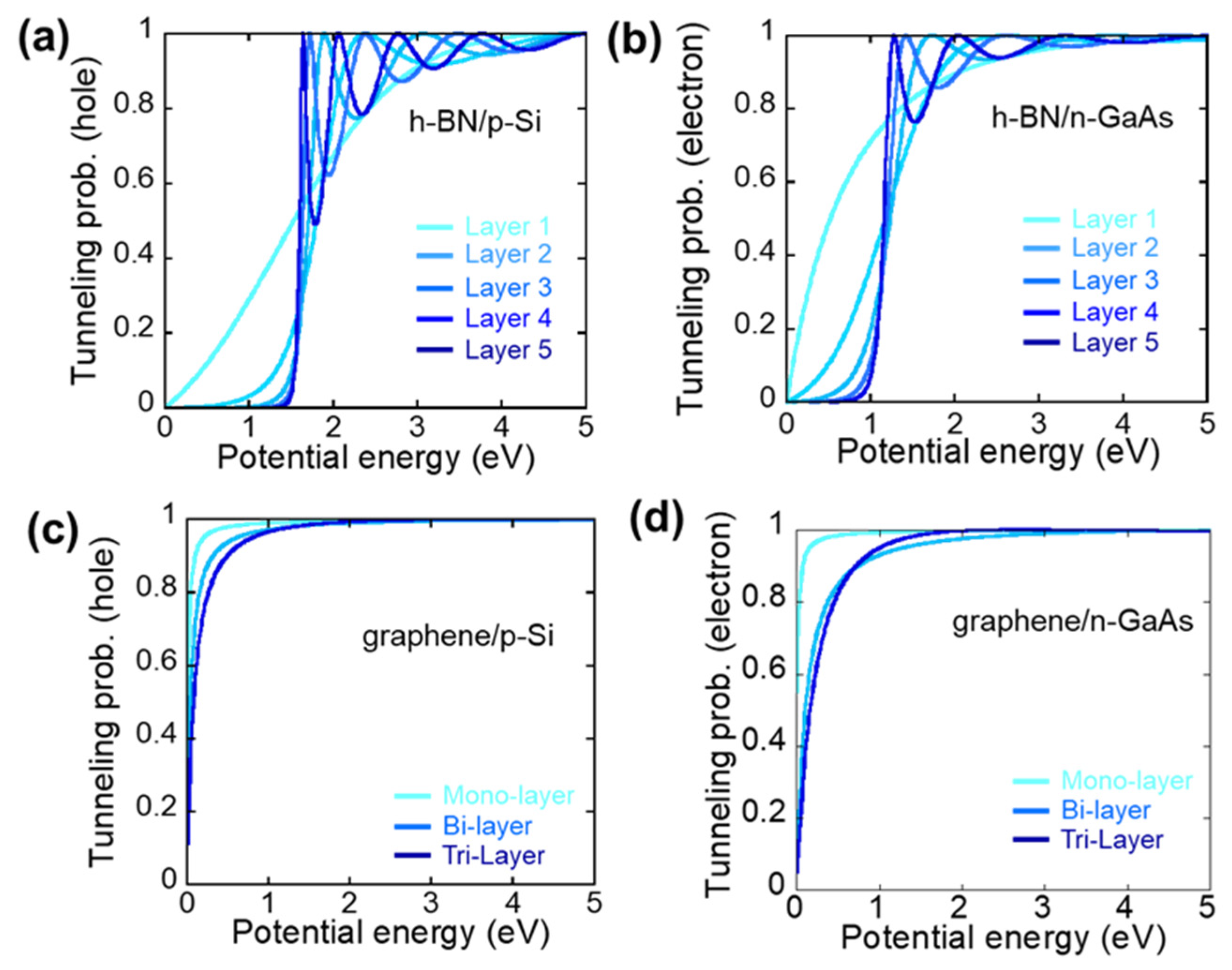
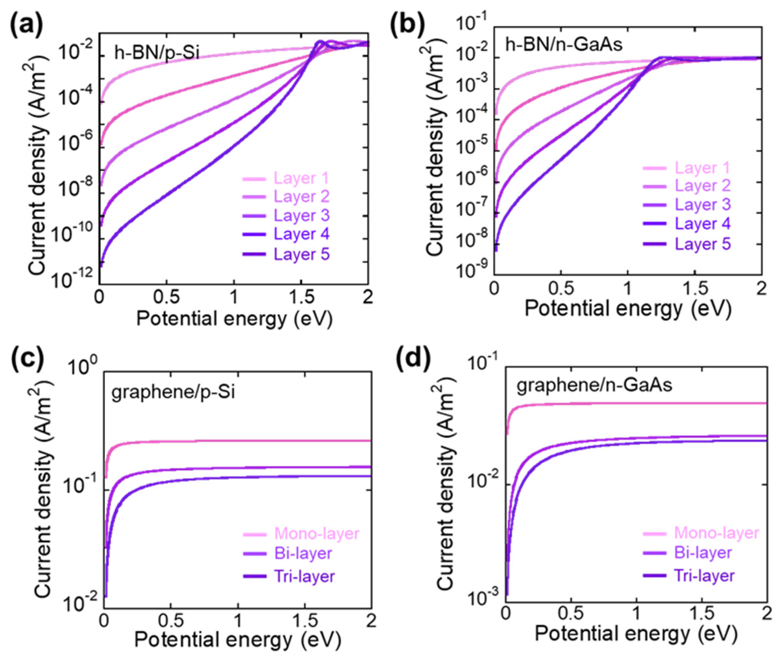
3.2. Tunneling Probability and Current Density with 2D Interface Layers

We further investigated two promising 2D material-based tunneling layers: h-BN and graphene. These two materials have completely opposite material properties including bandgap (0 eV for graphene vs. 5.97 eV for h-BN), effective mass (~0.01 m0 for graphene vs. >0.2 for h-BN), and doping (highly conductive for graphene vs. semi-insulating for h-BN) [27,28,29]. Therefore, a comparison of the tunneling properties and tunneling current using these two materials offers a material selection guideline among the numerous 2D materials. The parameters for graphene and h-BN can be found in the Supplementary Materials (Table S1). Figure 4a,b presents the hole and electron tunneling probability of h-BN/p-Si and h-BN/n-GaAs. The tunneling probability shows a similar trend to other oxide tunneling materials. This might be attributed to a wide bandgap (5.97 eV) and a similar range of barrier heights with oxides [30]. Interestingly, the tunneling structures using h-BN show more resonant tunneling peaks than the oxide-based tunneling structures due to its larger effective mass. Figure 4c,d shows the hole and electron tunneling probability of graphene/p-Si and graphene/n-GaAs. Graphene has unique material properties: It is tunable and has an energy bandgap close to zero. It has the lightest effective mass, etc. The very conductive nature of monolayer graphene could be highly efficient for carrier transport across the heterostructure. Although the tunneling probability is reduced with an increased layer thickness (tri-layer), the tunneling probability remains very high due to the negative band offsets with Si and GaAs.
The current density with the h-BN and graphene tunneling layer were also calculated using the same method as the oxide tunneling structures. This predicts their transport properties, as shown in Figure 5. The calculated current density decreased with increasing graphene thickness. The reduced current density is shown in Figure 5a,b up to the five-layered h-BN. Figure 5c,d shows the current density vs. potential energy plots with the monolayer, bilayer, and trilayer graphene. The highest tunneling current density shown in the graphene case might be attributed to the smallest bandgap and lightest effective masses. However, the formation of the quantum well with the graphene case might cause problems for specific devices based on quantum barrier/wells or carrier transport along with heterointerfaces because the graphene layer can trap the carriers, which leads to high interface defects.

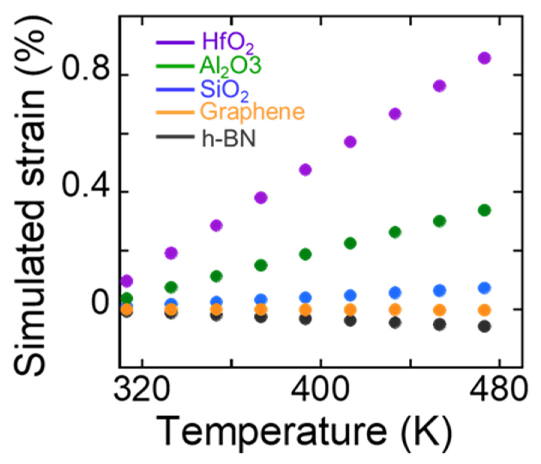
3.3. Simulated Strain under Temperature

Besides the transport property across the heterojunction, it is important to evaluate the changes in the strain of the tunneling layer under different temperature conditions. Smaller strains at the tunneling layer offer more reliable heterogeneous integration between two dissimilar semiconductors that typically have different thermal expansion coefficients. To investigate the evolution of the strain at the tunneling layer under different temperature conditions, we performed multiphysics simulations with five n-GaAs/tunneling layer/p-Si models using h-BN, graphene, HfO2, Al2O3, and SiO2 and traced the strain of the tunneling layer from room temperature (300 K) to 200 °C (473 K) using COMSOLTM. Figure 6 summarizes the strain as a function of temperature for five tunneling layers (details of the simulation can be found in Figure S2 of the Supplementary Materials). While SiO2, h-BN, and graphene showed almost negligible degrees of the strain changes (<0.1%), HfO2 particularly experienced nearly ten times higher strain by heating. Given that the thermal expansion coefficient of HfO2 is much larger (6.0 µm/m-K) [31] compared with other tunneling layer materials (0.5 µm/m-K or less) [32], it is possible to conclude that HfO2 is not a favorable material for the tunneling layer because the HfO2 tunneling layer can cause layer delamination during the fabrication process or device operation by heating.
In addition, the processability is another important point that governs the selection of an effective tunneling interfacial layer. For example, SiO2 has a wider bandgap than other oxides in this study, but it has a lower dielectric constant. HfO2 suffers from crystallization at high temperatures due to fast diffusion of oxygen through the HfO2. This results in uncontrolled growth of interfacial layers [33]. Therefore, considering all electrical and mechanical characteristics of various interfacial layer materials, the ideal interfacial layer should have a small conduction and valence band offsets, small effective mass, and small difference in the thermal expansion coefficient to the to-be-bonded materials. Most of all, ideal interfacial materials should be formed by ALD or should exist as a 2D format because they require atomic scale thickness control for the perfect surface coverage.

4. Conclusions

In conclusion, we built a numerical p-n Si/GaAs heterojunction model using quantum-mechanical tunneling theory with various quantum tunneling interfacial materials including 2D materials such as hexagonal boron nitride (h-BN) and graphene, and ALD-enabled oxide materials such as HfO2, Al2O3, and SiO2. Their tunneling efficiencies and tunneling current with different thicknesses were systematically calculated and compared. In oxide tunneling materials, it is found that these oxide tunneling layers promote carrier transport across the Si/GaAs heterojunction as the barrier height becomes lower and the tunneling layer becomes thinner. This trend was observed in h-BN as its’ barrier height and bandgap are in a similar range. In the case of graphene, although the tunneling probability remains very high at graphene/Si and graphene/GaAs, the formation of the quantum well due to the negative band offsets with Si and GaAs might cause problems for specific devices because the graphene layer may lead to high interface defect density, which is associated with a charge trap at the interface. In addition, multiphysics modeling was used with the aforementioned tunneling interfacial materials to analyze changes in the strain under different temperature conditions. Considering the transport properties and thermal-induced strain analysis, Al2O3, among three oxide materials, and graphene in 2D materials are favorable material choices that offer the highest heterojunction quality. Overall, our results offer a viable route in guiding the selection of ultra-thin tunneling intermediate materials for a myriad of possible combinations of new heterostructures. For instance, one can predict the feasibility of other materials as a hetero-interfacial layer. MoS2, as an example, has a relatively small conduction band offset to Si and a small valence band offset to GaAs. Additionally, the thermal expansion coefficient of MoS2 is much smaller than that of Si and GaAs. Thus, it is expected that the MoS2 UT layer works well with Si and GaAs with some degree of expansion force (tensile strain). Eventually, our results provide scientific insight in solving fundamental material challenges in the formation of various heterostructures and, thus, helps to establish a myriad of future functional heterostructures via a UT method.

Supplementary Materials

The following are available online at https://www.mdpi.com/article/10.3390/electronicmat2040034/s1. Figure S1: A schematic illustration of energy bandgaps, Figure S2: Simulated strain values, Table S1: Parameters for oxide and 2D materails used in calculations.

Author Contributions

All of the authors performed the research. J.-H.S. conceived the idea and designed and managed the research. M.N.H., C.L. and J.L. conducted the experiments. M.N.H. and J.-H.S. wrote the paper. All of the authors have read and agreed to the published version of the manuscript. All authors have read and agreed to the published version of the manuscript.

Funding

This work was supported by the National Science Foundation (grant number: ECCS—1809077) and partially by a seed grant by the Research and Education in Energy, Environment, and Water (RENEW) Institute at the University at Buffalo.

Institutional Review Board Statement

Not applicable.

Informed Consent Statement

Not applicable.

Data Availability Statement

The data underlying this article will be shared on reasonable request from the corresponding author.

Conflicts of Interest

The authors declare no conflict of interest.

References

  1. Liu, D.; Cho, S.J.; Park, J.; Gong, J.; Seo, J.-H.; Dalmau, R.; Zhao, D.; Kim, K.; Kim, M.; Kalapala, A.R. 226 nm AlGaN/AlN UV LEDs using p-type Si for hole injection and UV reflection. Appl. Phys. Lett. 2018, 113, 011111. [Google Scholar] [CrossRef]
  2. Sun, G.; Soref, R.; Cheng, H. Design of an electrically pumped SiGeSn/GeSn/SiGeSn double-heterostructure midinfrared laser. J. Appl. Phys. 2010, 108, 033107. [Google Scholar] [CrossRef]
  3. Dong, Y.; Son, D.-H.; Dai, Q.; Lee, J.-H.; Won, C.-H.; Kim, J.-G.; Kang, S.-H.; Lee, J.-H.; Chen, D.; Lu, H. AlGaN/GaN heterostructure pH sensor with multi-sensing segments. Sens. Actuators B Chem. 2018, 260, 134–139. [Google Scholar] [CrossRef]
  4. Ma, Z.; Seo, J.-H. Hybrid Heterostructure Light Emitting Devices. U.S. Patent 9,425,351, 23 August 2016. [Google Scholar]
  5. Palacios, T.; Chini, A.; Buttari, D.; Heikman, S.; Chakraborty, A.; Keller, S.; DenBaars, S.P.; Mishra, U.K. Use of double-channel heterostructures to improve the access resistance and linearity in GaN-based HEMTs. IEEE Trans. Electron Devices 2006, 53, 562–565. [Google Scholar] [CrossRef]
  6. Mapel, J.; Singh, M.; Baldo, M.; Celebi, K. Plasmonic excitation of organic double heterostructure solar cells. Appl. Phys. Lett. 2007, 90, 121102. [Google Scholar] [CrossRef] [Green Version]
  7. Yang, H.; Zhao, D.; Liu, S.; Liu, Y.; Seo, J.-H.; Ma, Z.; Zhou, W. Transfer printed nanomembranes for heterogeneously integrated membrane photonics. Photonics 2015, 2, 1081–1100. [Google Scholar] [CrossRef] [Green Version]
  8. Asif Khan, M.; Yang, J.; Knap, W.; Frayssinet, E.; Hu, X.; Simin, G.; Prystawko, P.; Leszczynski, M.; Grzegory, I.; Porowski, S. GaN–AlGaN heterostructure field-effect transistors over bulk GaN substrates. Appl. Phys. Lett. 2000, 76, 3807–3809. [Google Scholar] [CrossRef]
  9. Paul, D.J. Si/SiGe heterostructures: From material and physics to devices and circuits. Semicond. Sci. Technol. 2004, 19, R75. [Google Scholar] [CrossRef]
  10. Sandroff, C.; Nottenburg, R.; Bischoff, J.C.; Bhat, R. Dramatic enhancement in the gain of a GaAs/AlGaAs heterostructure bipolar transistor by surface chemical passivation. Appl. Phys. Lett. 1987, 51, 33–35. [Google Scholar] [CrossRef]
  11. Tong, Q.-Y.; Goesele, U. Semiconductor Wafer Bonding: Science and Technology; John Wiley: Hoboken, NJ, USA, 1999. [Google Scholar]
  12. Okuno, Y.; Uomi, K.; Aoki, M.; Tsuchiya, T. Direct wafer bonding of III-V compound semiconductors for free-material and free-orientation integration. IEEE J. Quantum Electron. 1997, 33, 959–969. [Google Scholar] [CrossRef]
  13. Black, A.; Hawkins, A.; Margalit, N.; Babic, D.; Holmes, A.; Chang, Y.-L.; Abraham, P.; Bowers, J.E.; Hu, E. Wafer fusion: Materials issues and device results. IEEE J. Sel. Top. Quantum Electron. 1997, 3, 943–951. [Google Scholar] [CrossRef]
  14. Pasquariello, D.; Hjort, K. Plasma-assisted InP-to-Si low temperature wafer bonding. IEEE J. Sel. Top. Quantum Electron. 2002, 8, 118–131. [Google Scholar] [CrossRef]
  15. Tanabe, K.; Watanabe, K.; Arakawa, Y. III-V/Si hybrid photonic devices by direct fusion bonding. Sci. Rep. 2012, 2, 1–6. [Google Scholar] [CrossRef]
  16. Howlader, M.; Watanabe, T.; Suga, T. Investigation of the bonding strength and interface current of p-Si/n-GaAs wafers bonded by surface activated bonding at room temperature. J. Vac. Sci. Technol. B Microelectron. Nanometer Struct. Process. Meas. Phenom. 2001, 19, 2114–2118. [Google Scholar] [CrossRef] [Green Version]
  17. Chung, T.R.; Yang, L.; Hosoda, N.; Takagi, H.; Suga, T. Wafer direct bonding of compound semiconductors and silicon at room temperature by the surface activated bonding method. Appl. Surf. Sci. 1997, 117, 808–812. [Google Scholar] [CrossRef]
  18. Liu, D.; Cho, S.J.; Seo, J.-H.; Kim, K.; Kim, M.; Shi, J.; Yin, X.; Choi, W.; Zhang, C.; Kim, J. Lattice-mismatched semiconductor heterostructures. arXiv 2018, arXiv:1812.10225. [Google Scholar]
  19. Cho, M.; Seo, J.-H.; Kim, M.; Lee, J.; Liu, D.; Zhou, W.; Yu, Z.; Ma, Z. Resonant cavity germanium photodetector via stacked single-crystalline nanomembranes. J. Vac. Sci. Technol. B Nanotechnol. Microelectron. Mater. Process. Meas. Phenom. 2016, 34, 040604. [Google Scholar] [CrossRef]
  20. Schenk, A.; Heiser, G. Modeling and simulation of tunneling through ultra-thin gate dielectrics. J. Appl. Phys. 1997, 81, 7900–7908. [Google Scholar] [CrossRef] [Green Version]
  21. Yoshida, T.; Imafuku, D.; Alay, J.L.; Miyazaki, S.; Hirose, M. Quantitative analysis of tunneling current through ultrathin gate oxides. Jpn. J. Appl. Phys. 1995, 34, L903. [Google Scholar] [CrossRef]
  22. Fermor, J. Quantum-mechanical tunneling. Am. J. Phys. 1966, 34, 1168–1170. [Google Scholar] [CrossRef]
  23. Chapter 1—Quantum Mechanical Tunnelling. In Tunnelling and Negative Resistance Phenomena in Semiconductors; Pamplin, B.R.; Roy, D.K. (Eds.) Pergamon: Oxford, UK, 1977; pp. 1–35. [Google Scholar]
  24. Thornton, S.T.; Rex, A. Modern Physics for Scientists and Engineers; Cengage Learning: Boston, MA, USA, 2012. [Google Scholar]
  25. Faddeev, L.D.; Merkuriev, S.P. Quantum Scattering Theory for Several Particle Systems; Springer Science & Business Media: Berlin/Heidelberg, Germany, 2013; Volume 11. [Google Scholar]
  26. Ghetti, A.; Liu, C.-T.; Mastrapasqua, M.; Sangiorgi, E. Characterization of tunneling current in ultra-thin gate oxide. Solid-State Electron. 2000, 44, 1523–1531. [Google Scholar] [CrossRef]
  27. Xu, Y.-N.; Ching, W. Calculation of ground-state and optical properties of boron nitrides in the hexagonal, cubic, and wurtzite structures. Phys. Rev. B 1991, 44, 7787. [Google Scholar] [CrossRef] [PubMed]
  28. Arnaud, B.; Lebègue, S.; Rabiller, P.; Alouani, M. Huge Excitonic Effects in Layered Hexagonal Boron Nitride. Phys. Rev. Lett. 2006, 96, 026402. [Google Scholar] [CrossRef] [PubMed] [Green Version]
  29. Avetisyan, A.; Partoens, B.; Peeters, F. Stacking order dependent electric field tuning of the band gap in graphene multilayers. Phys. Rev. B 2010, 81, 115432. [Google Scholar] [CrossRef] [Green Version]
  30. Liu, L.; Feng, Y.; Shen, Z. Structural and electronic properties of h-BN. Phys. Rev. B 2003, 68, 104102. [Google Scholar] [CrossRef]
  31. Haggerty, R.P.; Sarin, P.; Apostolov, Z.D.; Driemeyer, P.E.; Kriven, W.M. Thermal expansion of HfO2 and ZrO2. J. Am. Ceram. Soc. 2014, 97, 2213–2222. [Google Scholar] [CrossRef]
  32. El-Kareh, B.; Hutter, L.N. Fundamentals of Semiconductor Processing Technology; Springer Science & Business Media: Berlin/Heidelberg, Germany, 2012. [Google Scholar]
  33. Wilk, G.D.; Wallace, R.M.; Anthony, J. High-κ gate dielectrics: Current status and materials properties considerations. J. Appl. Phys. 2001, 89, 5243–5275. [Google Scholar] [CrossRef]
Figure 1. A schematic illustration of the semiconductor heterostructure formed by various ultra-thin tunneling intermediate layers: (a) oxide materials such as Al2O3, HfO2, and SiO2; (b) 2D materials such as h-BN and (c) graphene; and (df) their corresponding generic band diagrams.
Electronicmat 02 00034 g001
Figure 2. Tunneling probability of an electron across the UT interfacial layer with different thicknesses: (a) HfO2/n-GaAs, (b) Al2O3/n-GaAs, and (c) SiO2/n-GaAs; (df) tunneling probability of holes across these UT interfacial layers with p-Si with different thicknesses.
Electronicmat 02 00034 g002
Figure 3. (ac) Calculated current density of electrons and (df) holes with different oxide thicknesses across HfO2/n-GaAs, Al2O3/n-GaAs, and SiO2/n-GaAs.
Electronicmat 02 00034 g003
Figure 4. Tunneling probability of (a) a hole and (b) an electron across h-BN/p-Si and h-BN/n-GaAs with different h-BN thicknesses, and (c) a hole and (d) an electron across graphene/p-Si and gra-phene/n-GaAs with different graphene thicknesses.
Electronicmat 02 00034 g004
Figure 5. Calculated hole and electron current densities across (a) h-BN/p-Si, (b) h-BN/n-GaAs, (c) graphene/p-Si, and (d) graphene/n-GaAs with different thicknesses.
Electronicmat 02 00034 g005
Figure 6. Simulated strain (%) as a function of temperature for five interfacial layers (HfO2, Al2O3, SiO2, graphene, and h-BN) with different temperatures ranging from 300 K to 473 K.
Electronicmat 02 00034 g006
Publisher’s Note: MDPI stays neutral with regard to jurisdictional claims in published maps and institutional affiliations.

