Article

Ta2O5/SiO2 Multicomponent Dielectrics for Amorphous Oxide TFTs

1
i3N/CENIMAT, Department of Materials Science, NOVA School of Science and Technology and CEMOP/UNINOVA, NOVA University Lisbon, Campus de Caparica, 2829-516 Caparica, Portugal
2
IPFN, Instituto Superior Técnico, University of Lisbon, EN 10, km 139,7 2695-066 Bobadela, Portugal
*
Authors to whom correspondence should be addressed.
Electron. Mater. 2021, 2(1), 1-16; https://doi.org/10.3390/electronicmat2010001
Submission received: 11 November 2020 / Revised: 10 December 2020 / Accepted: 22 December 2020 / Published: 29 December 2020
(This article belongs to the Special Issue Feature Papers of Electronic Materials)

Abstract

:
Co-sputtering of SiO2 and high-κ Ta2O5 was used to make multicomponent gate dielectric stacks for In-Ga-Zn-O thin-film transistors (IGZO TFTs) under an overall low thermal budget (T = 150 °C). Characterization of the multicomponent layers and of the TFTs working characteristics (employing them) was performed in terms of static performance, reliability, and stability to understand the role of the incorporation of the high-κ material in the gate dielectric stack. It is shown that inherent disadvantages of the high-κ material, such as poorer interface properties and poor gate insulation, can be counterbalanced by inclusion of SiO2 both mixed with Ta2O5 and as thin interfacial layers. A stack comprising a (Ta2O5)x(SiO2)100 − x film with x = 69 and a thin SiO2 film at the interface with IGZO resulted in the best performing TFTs, with field-effect mobility (µFE) ≈ 16 cm2·V−1·s−1, subthreshold slope (SS) ≈ 0.15 V/dec and on/off ratio exceeding 107. Anomalous Vth shifts were observed during positive gate bias stress (PGBS), followed by very slow recoveries (time constant exceeding 8 × 10⁵ s), and analysis of the stress and recovery processes for the different gate dielectric stacks showed that the relevant mechanism is not dominated by the interfaces but seems to be related to the migration of charged species in the dielectric. The incorporation of additional SiO2 layers into the gate dielectric stack is shown to effectively counterbalance this anomalous shift. This multilayered gate dielectric stack approach is in line with both the large area and the flexible electronics needs, yielding reliable devices with performance suitable for successful integration on new electronic applications.

Graphical Abstract

1. Introduction

Amorphous oxide (AO) thin films have greatly progressed in a relatively short time, having found market application in the display industry where materials such as indium-gallium-zinc oxide (IGZO) appear as an advantageous alternative to Si technologies [1,2]. Besides conventional electronics, their characteristics make them suitable for concepts such as transparent and flexible electronics [3,4,5] or even paper electronics [6,7,8,9], allowing for interesting applications in fields such as medical, security and item tracking [10,11], crucial under the scope of the Internet of Things (IoT). One of the main advantages of AO is their good properties even when fabricated at low temperatures, with temperatures below 200 °C being imposed when considering flexible substrates or even paper substrates. Lower annealing temperatures unavoidably result in poorer device performance and stability. When considering these lower annealing temperatures the IGZO properties are known to be strongly related to its processing conditions [12] and adjustment of the cation ratio in the material thus plays a major role in its optimization [13]. In addition, employing dielectrics with high dielectric permittivity, εr, (high-κ dielectrics) can compensate for poorer performances by reducing driving voltages (e.g., as required in power-efficient applications within IoT) and improving gate voltage swing due to higher gate capacitances [14,15]. For low temperature deposition of dielectrics, physical techniques such as pulsed laser deposition (PLD) [16,17], thermal evaporation [18,19] and sputtering can be used, the latter allowing the deposition of most materials without any intentional substrate heating [20], at a large scale and with low contamination [21]. Several high-κ materials have been employed for gate dielectrics in low-temperature IGZO TFTs (or other ZnO-based TFTs) including: Al2O3 [22,23,24], HfO2 [25], Ta2O5 [26,27], Y2O3 [28,29,30] and ZrO2 [31]. Nevertheless, high-κ materials present some disadvantages, aggravated by low thermal budgets, when compared to conventional dielectrics such as SiO2. While having a relatively low permittivity (εr = 3.9), SiO2 is stable, has a very high band gap (Eg) of 9 eV and has a low defect density making it a good insulator with a high breakdown voltage. Additionally, it is amorphous and has a good interface with IGZO. On the other hand, ionic bonds in high-κ dielectrics result in high defect concentrations with oxygen vacancies (VO) being the primary source of traps. These can be a source of fixed charges or act as electron traps, scattering carriers in the channel (decreasing mobility), changing the threshold voltage (Vth) and assisting oxide breakdown and gate leakage mechanisms [32], decreasing device performance, stability and reliability. Furthermore, high-κ materials are often polycrystalline (even at low temperatures) with grain boundaries contributing both to degraded surface properties and acting as preferential paths for leakage current and impurity diffusion [33,34]. When choosing the dielectric material, band alignment should be considered as at least 1 eV of conduction/valence band offset is desirable for blocking electron/hole injection. εr is normally inversely proportional to Eg (Figure 1), and the band alignment of several dielectrics with IGZO can be found in the work of Hays et al. [35].
Incorporation of higher Eg materials with high-κ dielectrics effectively increases EG and can result in amorphous materials to much higher temperatures due to their increased disorder [36]. Regarding low temperature (T < 200 °C) ZnO-based TFTs with multicomponent dielectrics, sputtered Bi1.5Zn1.0Nb1.5O7 showed εr ≈ 51 but was polycrystalline at room-temperature (RT) [37] while sputtered Ba0.5Sr0.5TiO3 (εr ≈ 28) was amorphous at RT but presented significant leakage [38]. The insertion of MgO into the latter dielectric improved insulation at the expense of εr (to close to 18) and it was applied to IGZO TFTs with good performance on plastic substrates [39]. In previous studies conducted by our group, sputtered HfO2 was combined with SiO2 or AlOx effectively preventing the crystallization of the material at RT [20,40]. Similarly, Ta2O5 was combined with SiO2 or AlOx resulting in TFTs with good insulation and good performance at T ≤ 150 °C [14,27]. Another approach to reduce leakage is the use of multilayered gate dielectric stacks in which SiO2 layers (or other low defective materials) are employed at the dielectric/semiconductor interface. In general, these layers result in lower trap densities at the interface improving device performance and stability while imposing a higher barrier for carrier injection. Sputtered HfOxNy/HfO2/HfOxNy [41] and HfO2/SiO2 [21,42] stacks showed improved interface quality and insulation properties when compared to the respective single layer high-κ dielectrics. Hsu et al. showed excellent flexible IGZO TFTs fabricated at RT with electron beam evaporated SiO2/TiO2/SiO2 [43]. Solution based processes can also be used for depositing high-κ dielectrics such as HfO2, ZrO2, and Ta2O5, permitting devices with very good performance [44,45] and multilayered stacks with these processes were shown to be promising even when considering low temperatures (T < 150 °C), as shown by Carlos et al. [46], while others have shown that this approach can even improve mechanical flexibility [47]. While masking some of the high-κ dielectrics disadvantages, these approaches can significantly decrease the effective oxide εr. Moreover, while the multicomponent and multilayer concepts in dielectrics were already demonstrated, the dielectric layer composition and the gate dielectric stack architecture need to be carefully considered to obtain the best combination of performance and reliability. This is particularly relevant when imposing low thermal budgets (T ≈ 150 °C), given that in such cases the usual benefits of high temperature annealing to improve film quality cannot be considered. These low temperatures are extremely relevant in the current scenario of flexible electronics, where aspects such as hybrid integration with temperature sensitive technologies as organics or usage of unconventional substrates as paper are considered [7,11,48]. Within this context, this work presents a study of the effect of composition in multicomponent dielectric layers composed both by sputtered Ta2O5 (a high-κ dielectric with εr = 25) and sputtered SiO2. Besides having a high dielectric permittivity and an amorphous structure, Ta2O5 can be deposited by sputtering with a good growth rate without requiring the application of very high power [14]. A low thermal budget (T ≤ 150 °C) was considering in this work, for compatibility with flexible substrates. Multilayered stacks comprising these multicomponent layers and SiO2 layers were also studied and IGZO TFTs employing these dielectrics were assessed in terms of performance, stability, and reliability.

2. Materials and Methods

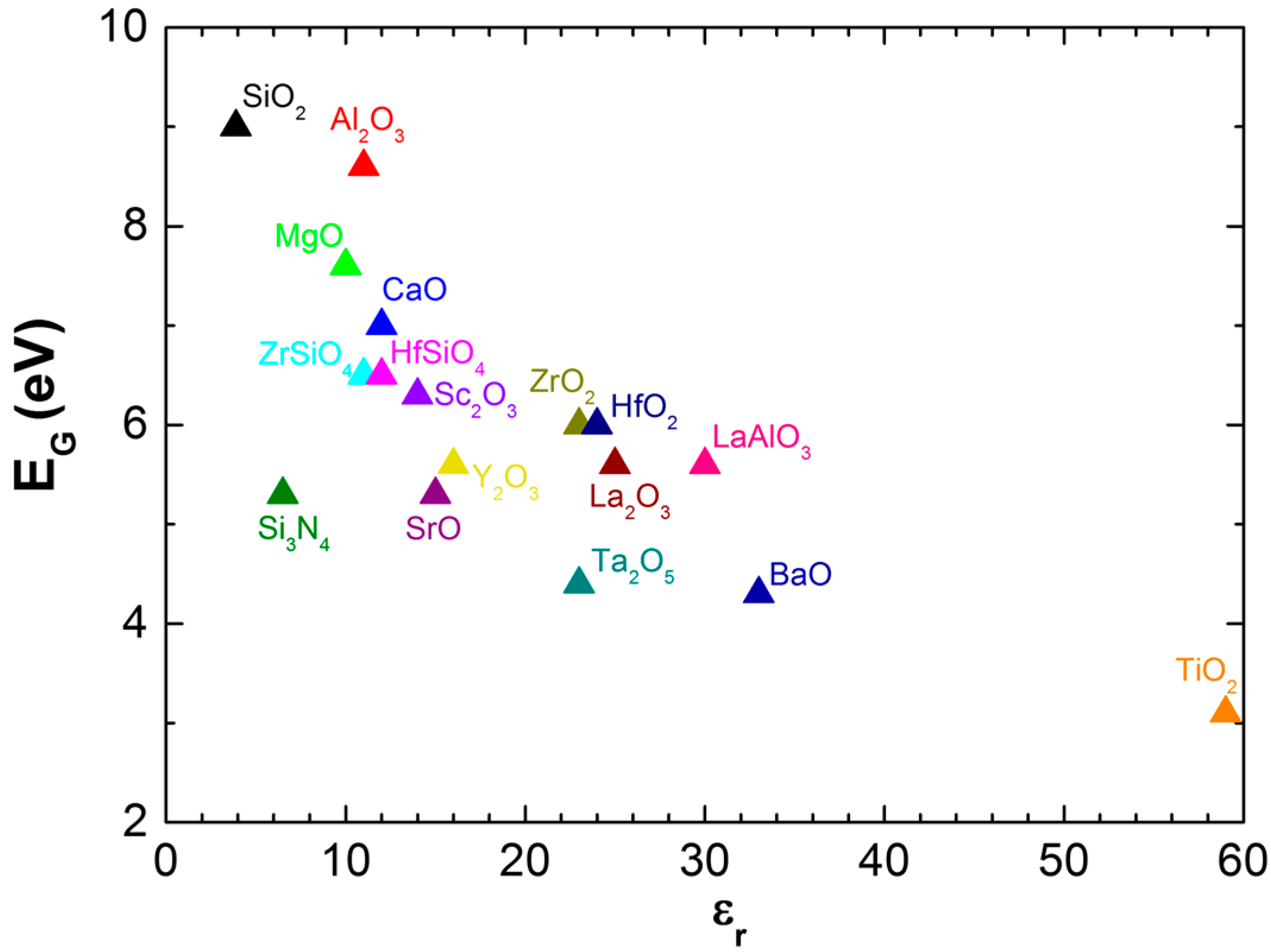
2.1. Device Fabrication

IGZO TFTs were fabricated with a staggered bottom gate structure on Corning glass by using standard photolithography patterning procedures, with UV patterning on a Suss MA6 aligner (SUSS MicroTec, Garching, Germany). All layers were produced by radio frequency (RF) magnetron sputtering in an AJA ATC-1300F system (AJA International Inc., North Scituate, MA, USA) without intentional substrate heating. The gate electrodes were sputtered from a Mo target in an oxygen free atmosphere with an RF power density of 3.8 W/cm2 resulting in a final thickness of 60 nm. The multicomponent dielectric films were produced by co-sputtering from 2 inch ceramic targets of Ta2O5 and SiO2 under an argon + oxygen atmosphere and the power applied to the Ta2O5 target was varied between 50 and 150 W, while power of 150 W to the SiO2 target was kept fixed, resulting in films with different Ta2O5:SiO2 contents. A substrate bias of 84 V during the dielectric depositions was used as it is known to result in denser and smoother films [21]. A dielectric film of only Ta2O5 was also produced for investigating the role of the SiO2 incorporation in the high-κ dielectric stacks. The 40 nm semiconductor film was sputtered from a 2 inch multicomponent ceramic target of IGZO 2:1:2 (In2O3:Ga2O3:ZnO mol) with an RF power density of 4.9 W/cm2 in an argon + oxygen atmosphere, resulting in an amorphous film with a 4:2:1 (In:Ga:Zn) atomic ratio [49]. The source and drain electrodes were sputtered in the same way as the gate dielectric. All layers were patterned by lift-off technique with the exception of the dielectric which was patterned by plasma etching in SF6 atmosphere. Resulting TFTs had a width-to-length ratio (W/L) of 320/20 (μm/μm). The devices were annealed on a hot plate at 150 °C for 1 h. A schematic of the device cross-section is shown in Figure 2a. For capacitance analysis, metal-insulator-semiconductor (MIS) devices with the same dielectric layers were produced using p-type Si wafers as substrates and Mo top contacts with areas of 1.88 × 10⁻³ cm2. The multicomponent dielectrics were also deposited in p-type Si wafers for Rutherford backscattering spectrometry (RBS) for compositional analysis and for spectroscopic ellipsometry (SE).
Additionally, devices employing gate dielectrics consisting of a stack of a multicomponent layers and a SiO2 layer where also fabricated. In these stacks the multicomponent layer was produced with a power of 100 W in the Ta2O5 target and a power of 150 W in the SiO2 target, with expected thickness of 200 nm for this layer. The SiO2 layer in these stacks is employed either at the gate/dielectric interface or at the dielectric/semiconductor interface by sputtering with a power of 150 W before or after the multicomponent layer, respectively, and without breaking vacuum during the entire dielectric stack deposition, with a nominal thickness of 15 nm for the SiO2 layer. These dielectric stacks and the multicomponent single layer dielectrics are schematized in Figure 2a.

2.2. Films and Devices Characterization

The stoichiometry of the dielectrics was assessed by Rutherford backscattering spectrometry (RBS) using a 2 MeV He beam delivered by a 2.5 MV van de Graaf accelerator. Two solid state detectors placed at 140° and 165° were used to collect the backscattered particles. The RBS spectra were analyzed with IBA DataFurnace NDF software [50]. A HORIBA-Jobin Yvon spectroscopic ellipsometry system was used with an incident angle of 70° in a spectral range between 1.5 and 6.5 eV. The acquired data was analyzed with DeltaPsi 2 software (v2.6.6.212, Horiba, Bensheim, Germany) and fitted using the Tauc–Lorentz dispersion formula [51]. TFTs and MISs were characterized using a Keysight B1500A (Keysight Technologies, Santa Rosa, CA, USA) semiconductor parameter analyzer in a EPS 150 probe station (Cascade Microtech, Beaverton, OR, USA). The MIS devices were characterized through capacitance–voltage (C-V) analysis at 100 kHz.

3. Results and Discussion

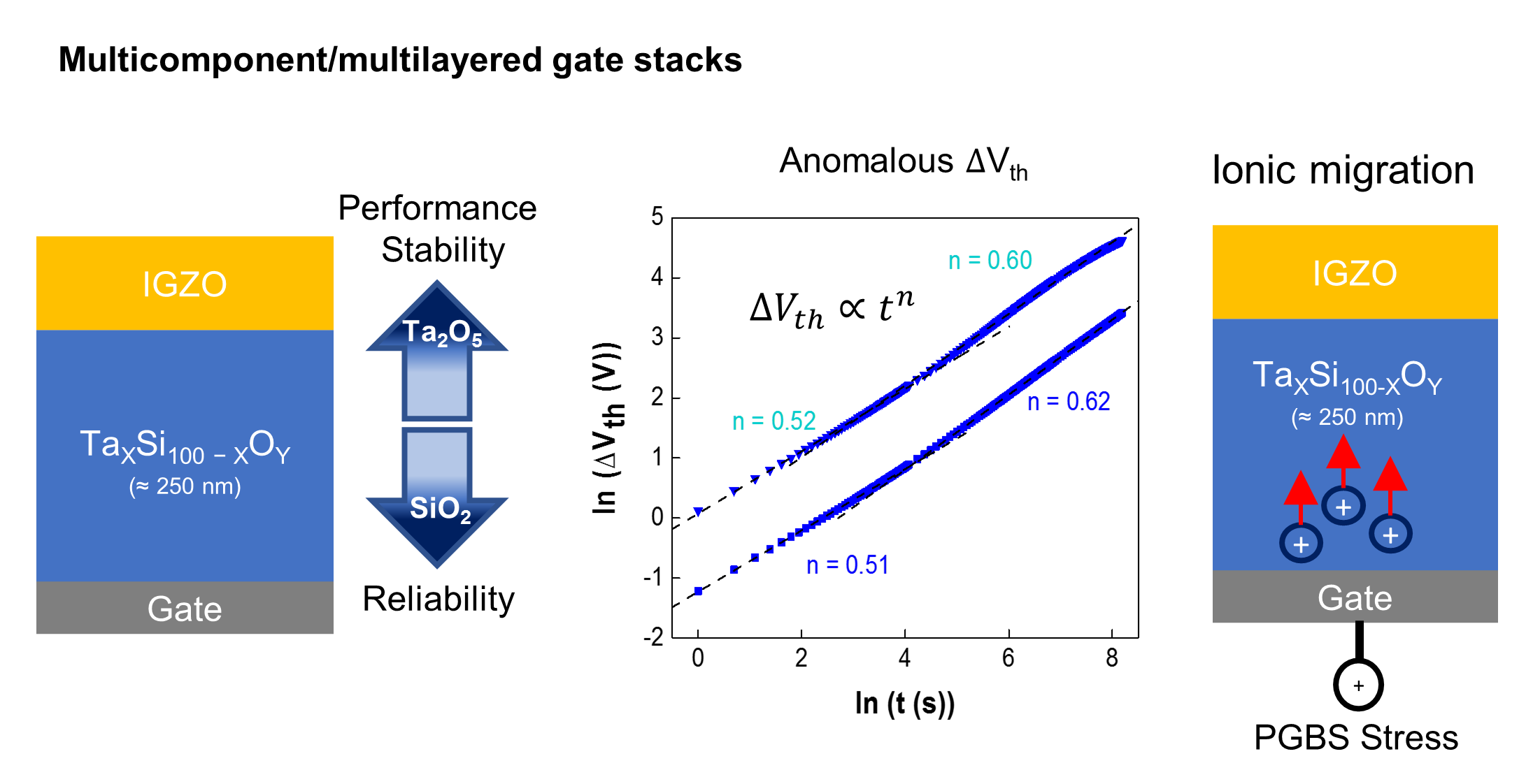
3.1. Multicomponent Dielectric Properties

RBS analysis was performed on the multicomponent films sputtered with different powers applied to the Ta2O5 target. The RBS spectra are presented in Figure 2b, in which the barrier for each element is indicated by vertical arrows. It is noticeable that with the increase of the power in the Ta2O5 target the Ta barrier height increases whereas the Si barrier decreases. Analysis of this data allowed assessing of the stoichiometry of the films, confirming the different Ta2O5 and SiO2 contents within the dielectrics as summarized in Table 1. RBS revealed some incorporation of Ar (values presented in Table S1) across all film compositions, as is common for films sputtered in Ar rich atmospheres [52]. Figure S1 presents the Ar content in the dielectric for different Ta2O5 contents, showing clearly that the Ar incorporation is more pronounced for higher Ta2O5 contents. Nevertheless, the Ar content across all compositions (4.3 ± 0.7%) does not change significantly (from 3.4% to 5.5%) and the Ta2O5 and SiO2 contents presented in Table 1 are thus normalized to 100%, for simplicity. According to the normalized Ta2O5 and SiO2 compositions the multicomponent dielectric layers are denominated as “TxS100 − x” where x is the approximate Ta2O5 percentage of the material, and 100 x is thus the approximate SiO2 percentage. “T” and “S” thus correspond to Ta2O5 and SiO2, respectively, under this nomenclature. For clarity, when the dielectric is based on a single cation, the usual chemical formulas are employed, namely, Ta2O5 or SiO2. For each of these layers its thickness was extracted from the analysis of the SE data, with values in the 200−250 nm range [53]. As for the multilayered gate dielectric stacks, their multicomponent layers have “T69S31 composition and are then denominated “SiO2/T69S31” and “T69S31/SiO2”, according to the position of the SiO2 layer in the gate dielectric stack, as schematized in Figure 2a.
Knowing the areal density extracted from RBS and the thicknesses from SE (Table S1), the atomic density for each composition can be calculated. It was shown in a previous work that at least for the range of power used here, the Ta2O5 density is independent of the power density in the Ta2O5 target [53] and since the SiO2 target power density is kept for all compositions, the atomic densities for each composition can be assumed to depend linearly on the content of each material as per (1)
ρ = ρ T a 2 O 5 . x + ρ S i O 2 ( 100 x ) = ( ρ T a 2 O 5 ρ S i O 2 ) . x + ρ S i O 2
where the approximate percentages of Ta2O5 and SiO2 are x and 100 x , respectively. Figure 2c shows the atomic density for the different dielectric compositions. From the linear fitting of the data, the oxides’ atomic densities are estimated as ρ S i O 2 = ( 6.40   ±   0.10 ) × 10 22 cm−3 and ρ T a 2 O 5 =   ( 7.74   ± 0.17 )   × 10 22 cm−3 which are below only 3.3% and 1.1% of the theoretical values, respectively, assuming mass densities of 2.2 g·cm−3 for SiO2 [54] and 8.2 g·cm−3 for Ta2O5 [55].
Regarding surface roughness, SiO2 films are known to be smooth and even with the increase of Ta2O5 content in the multicomponent material, ellipsometry and AFM showed that these films are still smooth with T69Si31 layers and Ta2O5 films presenting roughness below 0.5 nm and 1.1 nm, respectively [53,56]. Furthermore, XRD characterization showed that these films are amorphous up to 900 °C [56].
From the C-V characterization of the MIS structures (Figure S2), the dielectric permittivity (εr) was calculated for the different multicomponent dielectrics, as presented in Figure 2d and in Table 1. As expected, by incorporating Ta2O5 the dielectric constant can be greatly increased when compared to that of pure SiO2. Assuming that εr depends linearly on the content of each material as per (2)
ε r = ε r , T a 2 O 5 . x + ε r , S i O 2 ( 100 x ) = ( ε r , T a 2 O 5 ε r , S i O 2 ) . x + ε r , S i O 2
where x and 100 x are the approximate percentages of Ta2O5 and SiO2, respectively, each oxides’ permittivity can be estimated as ε r , S i O 2 = 1.29 ± 1.06 and ε r , T a 2 O 5 = 22.48 ± 1.82 from the linear fitting of the data. These values are relatively lower than the theoretical permittivities (3.9 and 25, respectively) which can be attributed to the defective structure of low-temperature sputtered oxide dielectrics. This is especially noticeable for the SiO2′s dielectric constant, highlighting the significance of the Ta2O5 incorporation as a method for achieving reasonable dielectric permittivities. Regarding the multilayered stacks, while employing SiO2 layers, they in fact have a capacitance between that of the T69S31 and the T75S25 gate dielectric stacks and result in effective dielectric permittivities close to that of the T69S31 gate dielectric stack.

3.2. Device Characterization

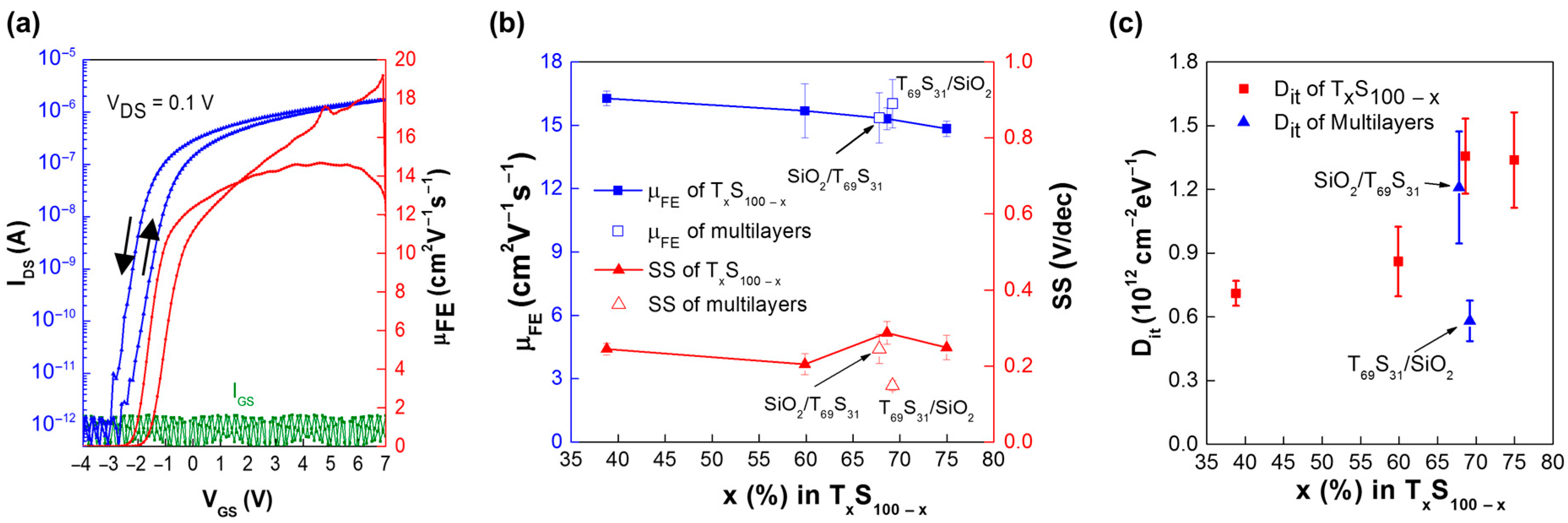
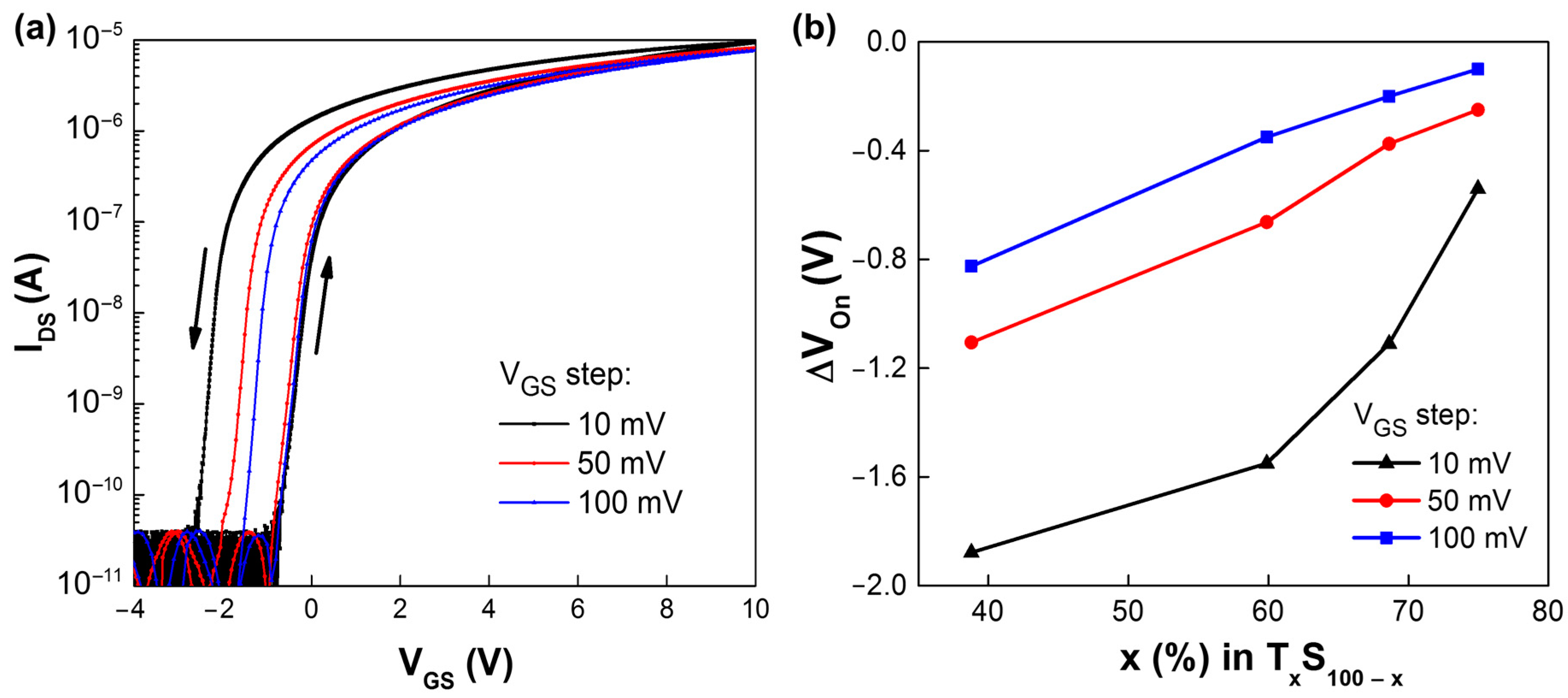
3.2.1. TFT Performance

The performance of TFTs employing the different dielectric compositions was evaluated and a transfer curve for the T60S40 composition is presented in Figure 3a as an example. Figure 3b summarizes the field-effect mobilities (μFE) and subthreshold slopes (SS) obtained with the different TxS100 − x dielectrics. With the addition of Ta2O5 content, a slight degradation of the mobility from ≈ 16.3 to 14.8 cm2·V−1·s−1 is observed. This can be justified by the decrease of quality of the TxS100 − x/IGZO interface with the addition of Ta2O5, where defects such as fixed charges can cause the scattering of carriers, decreasing their mobility. The trap density at the interface (Dit) was extracted from (3) in which k, T, and e have their usual physical meanings and C is the dielectric capacitance.
S S l n ( 10 ) k . T e ( 1 + e . D i t C )
As presented in Figure 3c, D i t tends to increase with the addition of Ta2O5 content, showing that the high-κ oxide results in poorer interface quality with IGZO when compared to SiO2. Nevertheless, for the studied range of Ta2O5 incorporation, all the devices show good performance with mobilities above 14 cm2·V−1·s−1, SS lower than 0.3 V/dec, on/off ratios close to 1 × 10⁷ and gate leakage currents (IG) close to 1 pA. Regarding the devices employing the multilayered gate-stacks, for the SiO2/T69S31, dielectric properties close to that of the T69S31 were found, which should be related to the similar T69S31/IGZO interface. For the TFTs employing a T69S31/SiO2 layer, mobility was slightly higher than most TxS100 − x compositions, and a great improvement is shown in SS (0.15 V/dec) and consequently Dit, showcasing the significantly better quality of the SiO2/IGZO interface.

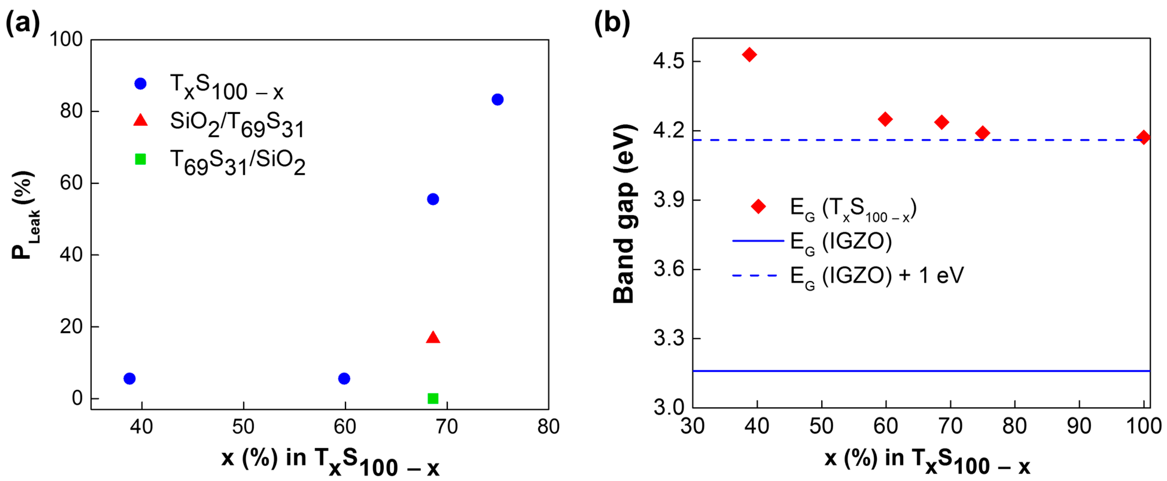
3.2.2. Insulation Reliability
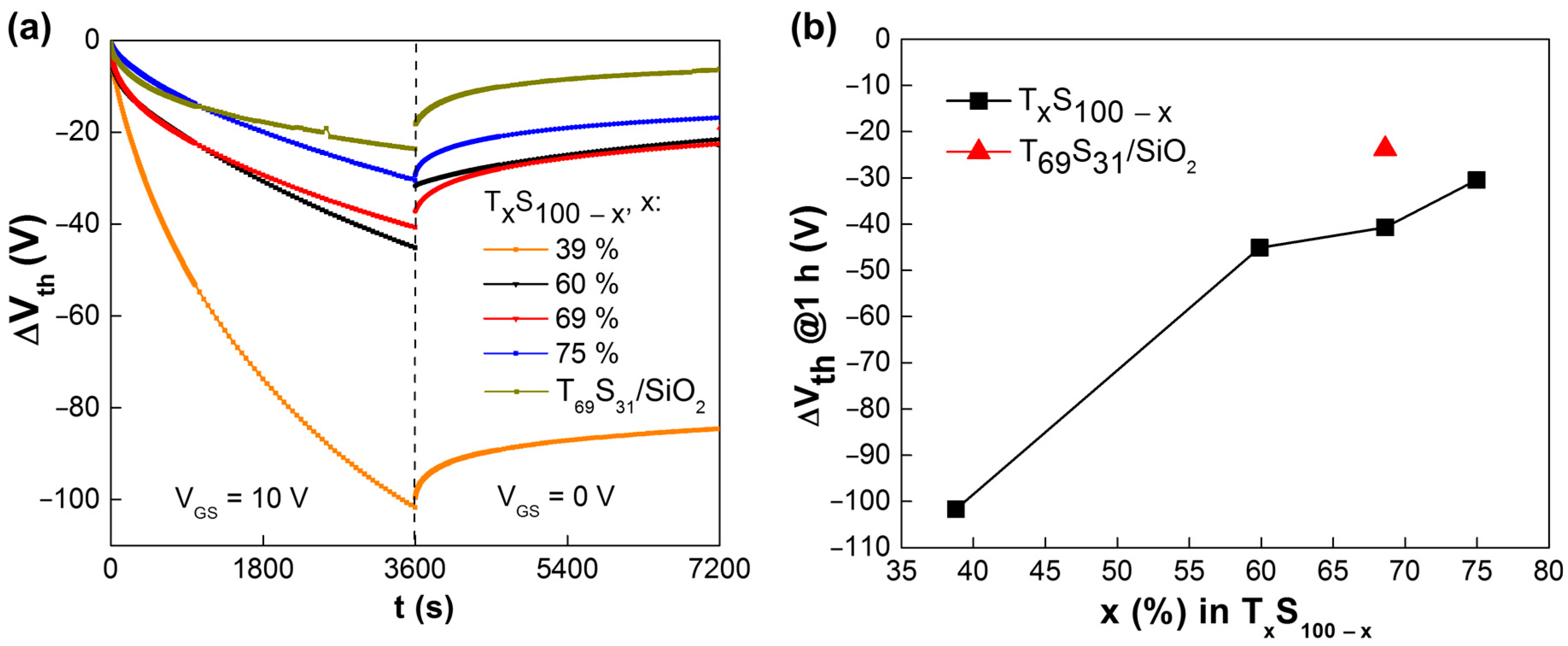
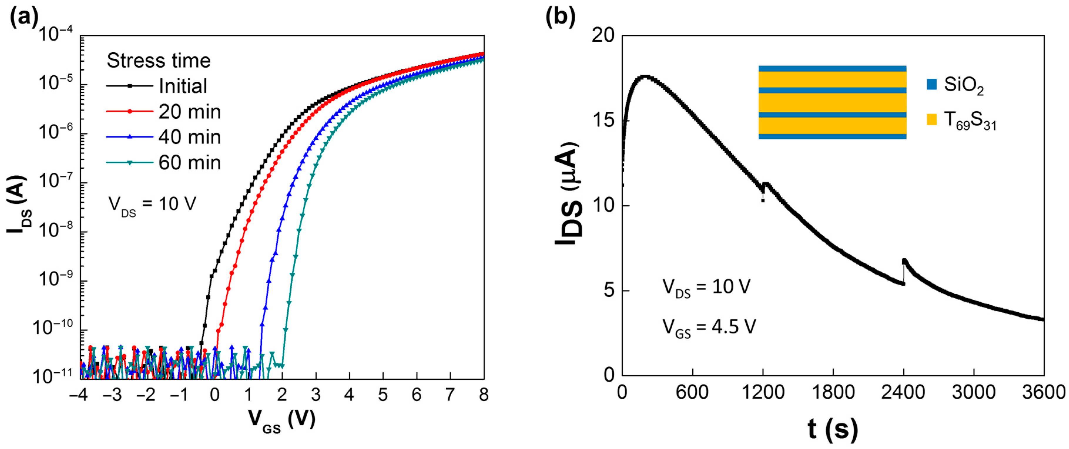
Arising from higher defect densities and lower band gaps, employing high-κ dielectrics can often result in high IG. In fact, TFTs employing a Ta2O5 dielectric layer revealed poor insulation which compromised the extraction of their transfer characteristics. Regarding the TxS100 − x dielectrics, while IG was below 1 pA for TFTs considered to be working properly (see Figure 3a), in some devices an abrupt increase of IG is seen with the increase of gate voltage. To quantify the dielectric reliability for each TxS100 − x composition (and for the multilayered structures), a leakage probability (PLeak) was determined as the frequency of TFTs presenting gate leakage out of 18 similar devices. In practice, IG was either in the noise level (for properly working TFTs) or higher than several nA (considered as leakage). Figure 4a presents the leakage probability for TFTs with channel widths and lengths of 320 μm and 20 μm, respectively.
Whereas a good reliability is seen for Ta2O5 contents of 60% and lower, it decreases abruptly for contents of 69% and higher. This can be attributed either to an increase of the conductivity of the dielectric layer or to a decrease of the conduction band offset (∆EC) between IGZO and the dielectric layer, allowing the injection of carriers into the dielectric trough conduction mechanisms such as thermionic emission and field emission [57]. The band gaps of the TxS100 − x dielectrics, obtained from ellipsometry measurements [53] are shown in Figure 4b. For all compositions, the band gaps are much closer to that of Ta2O5 (≥4 eV [58,59]) than that of SiO2 (8.9 eV), a trend that has been seen before for other high-κ/SiO2 mixtures [14,20,35]. Nevertheless, the increase of band gap with the incorporation of SiO2 is still relevant: to block charge injection, a conduction band offset above 1 eV is desirable and while the valence band offset to IGZO is unknown, the measured TxS100 − x band gaps are very close to 1 eV above the IGZO’s band gap (as represented in Figure 4b). This means that the slight band gap increase by the incorporation of SiO2 may play a critical role in blocking the injection of charge. Leakage probabilities for the multilayered dielectrics are also presented in Figure 4a, and these are compared to the T69S31 single layer. The SiO2 layer at the gate/dielectric interface (SiO2/T69S31) significantly reduces the leakage probability, demonstrating the good insulation properties of this stack. Nevertheless, with the SiO2 layer at the dielectric/IGZO interface (T69S31/SiO2), this is even further enhanced, with no leaking devices being found. Compared to the SiO2/T69S31 layer, this improvement can be attributed to a decrease of charge injection from the IGZO to the gate dielectric stack (e.g., hot electron injection) due to either the higher ∆EC, better interface quality, or both. This shows that multilayered gate dielectric stacks are a viable approach to improve device performance without sacrificing reliability.

3.2.3. Stability

It is interesting to notice that the transfer curves for these devices present counterclockwise hysteresis. When employing SiO2 dielectrics the hysteresis is known to be clockwise resulting from electron trapping in the dielectric/semiconductor interface trap-sites. Nevertheless, this counterclockwise hysteresis has been previously reported at times for some high-κ dielectrics, as will be discussed later. This device hysteresis was shown to increase with decreasing VGS step (which increases measurement time) as shown in Figure 5a for the T60S40 composition. Considering VOn the VGS for IDS ≈ 100 pA, the measured hysteresis (∆VOn) for different VGS steps for the different TxS100 − x compositions is presented in Figure 5b. Counterintuitively, the hysteresis is higher (in magnitude) for higher SiO2 content and this will be addressed later. As for the multilayered gate dielectric stacks, the hysteresis was shown to be close to that of the corresponding single layer (T69S31), even in the case of a SiO2/IGZO interface.
The hysteresis’ direction is usually tied with the direction of the Vth shift seen during positive gate bias stress (PGBS), unless different mechanisms play a role in these [60]. TFTs with the different dielectrics where submitted to PGBS with a gate voltage of 10 V for 1 h, followed by 1 h of recovery at VGS = 0 V. During both, a drain voltage of 0.1 V was applied allowing addressing of the value of Vth by (4), which was fairly consistent with the Vth extracted from transfer curves before and after stress and recovery.
I D S = μ F E C o x W L ( ( V G S V t h ) V D S V D S 2 2 )
The threshold voltage shift (∆Vth) for the different compositions is shown in Figure 6a. Similarly to the devices’ hysteresis, Vth also shifts towards more negative values during PGBS, as opposed to the typically reported positive Vth shift associated with electron trapping at the interface. Vth shifts with higher magnitude are once again observed for the SiO2-richer compositions, as summarized in Figure 6b. Interestingly, in the same time frame, Vth shows only a partial recovery (for VGS = 0 V), unlike in the faster relaxations typical of cases dominated by electron (de)trapping, whereas applying a negative gate bias (VGS = −10 V) resulted in a fast recovery of the threshold voltage (Figure S3a).
In Figure 6b, the Vth shift for the T69S31/SiO2 layer is also shown. While its shift magnitude is significantly lower than that of the TxS100 − x/IGZO interfaces, it is still negative, suggesting that this anomalous shift is not an interface phenomena and it is in competition with the electron-trapping at the SiO2/IGZO interface during the PGBS [60].
Considering conventional applications (for which Vth shifts are undesirable), Ta2O5-richer compositions present as better alternatives both by resulting in higher dielectric permittivities and for lower Vth shifts. While these compositions can be unreliable in terms of gate leakage, it was demonstrated that thin SiO2 layers at the dielectric/semiconductor interface successfully prevent gate leakage even for thinner overall gate dielectric stacks (with effectively higher capacitances). This shows that the multicomponent and multilayered approach can be a feasible method for achieving high device performance by incorporation of high-κ dielectrics without sacrificing device reliability. In fact, while the presented Vth shift magnitudes are considerably high, further addition of SiO2 layers can be used to counterbalance this anomalous shift. This approach permits achieving devices with lower and positive Vth shift magnitude, while still maintaining desirable values for effective εr of 10–15. This is shown in Figure 7, for devices previously reported by our group [60] which employed similar multilayered gate dielectric stacks with an increased number of SiO2 layers as shown in the inset of Figure 7b, resulting in εr ≈ 13. While positive Vth shifts in transfer curves measured after discrete periods of gate bias stress suggest the charge trapping mechanism only (Figure 7a), closer inspection along the duration of the stress by monitoring the drain current (Figure 7b) allows observing that the anomalous shift of Vth occurs during the first few minutes of stress. This clearly shows that the two mechanisms are in competition with charge trapping dominating, eventually resulting in an overall Vth shift of 1.3 V after 1 h of bias stress. Similar devices were successfully applied for a flexible radiation sensing system, both for timing signals generation for addressing the sensors in the irradiated matrix [61] and for a high-gain transimpedance amplifier for amplification and voltage transduction of the sensors current signal [10], with both implementations requiring robust device operation.

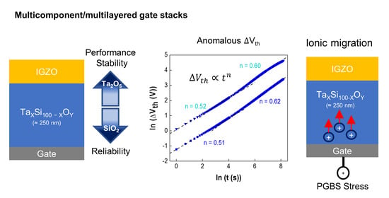
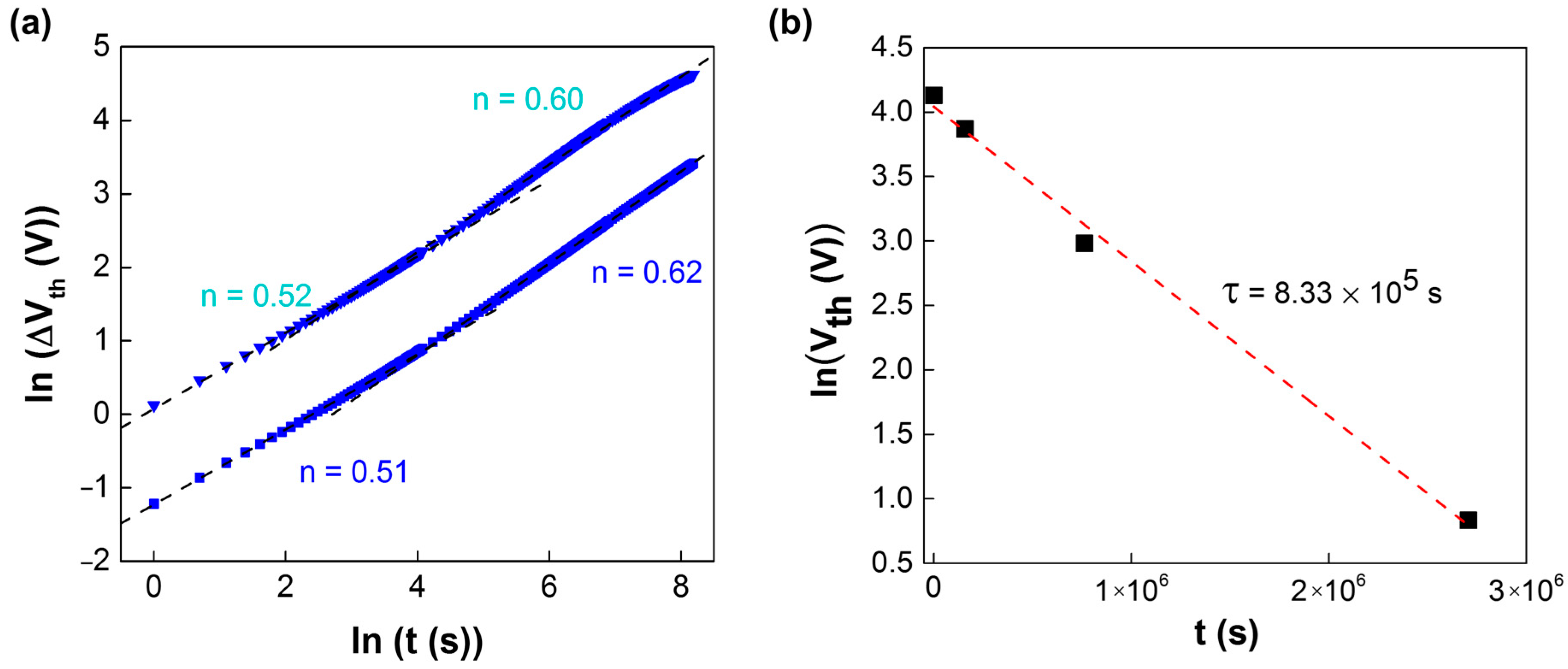
3.3. Mechanism of the Anomalous Vth Shift

A discussion of the mechanisms involved in the observed anomalous Vth shifts is now presented. While these have been reported for TFTs employing high-κ gate dielectrics (such as Ta2O5 [62,63,64], ZrO2 [9] and HfO2 [65]), other reports often show normal shift directions. High-κ dielectrics are known to be prone to have high defect density (probably playing a role in the anomalous shift) and it should be expected that different processing methodologies can result in distinct material qualities, leading to different device behaviors. The mechanisms that are normally used to explain anomalous Vth shifts [34] are: charge (de)trapping from the gate dielectric [62,65] ionic migration within the dielectric [63] (understandable as a slow polarization of the dielectric material [64]) and defect creation [66]. Regarding defect creation, it can lead to an increase in the carrier concentration, resulting in the decrease of the Vth, and it was shown before for poor quality semiconductors [66]. In this case, this can be disregarded as no change in the transfer curves’ SS was observed, demonstrating the stability of the semiconductor (even considering the low thermal budget employed here). Furthermore, it is expected that the involved mechanism is dielectric related as this anomalous shift is not observed in our IGZO TFTs when employing other dielectrics. Regarding the charge trapping mechanisms, a positive net charge change is required for a negative Vth shift. Hole trapping at the dielectric/semiconductor interface can be disregarded as the voltage polarity is opposite to what would be required, and wide band gap n-type oxides require optical excitation for holes to be generated in the first place. Then, electron detrapping from the dielectric to the gate must be considered (e.g., from negatively charged oxygen interstitials: IO or IO2– [65]). However, detrapping at this interface cannot change the electron concentration at the semiconductor, and thus cannot explain the anomalous shift if charge migration is not assumed [34,64]. To investigate the mechanism, the time dependency of the threshold voltage shift during the gate bias stress was studied and a power-law dependence ( Δ V t h t n ) was found, as shown in Figure 8a for the T39S61 and T75S25 compositions. While exponential dependencies are seen when charge (de)trapping is the relevant process, power dependencies are often related to reaction–diffusion mechanisms. For the compositions presented in Figure 8a, the exponent n changed from ≈0.5 to ≈0.6 after approximately 1 min. For the intermediate TxS100 − x compositions, the exponent changed from ≈0.33 to ≈0.5 after approximately 1–5 min (Figure S4a,b). Similar dependencies were noted for the multilayered stacks (Figure S4c), further suggesting that the mechanism is not dominated by either of the interfaces. Power law time dependency of Δ V th is known for the diffusion of H species in MOSFETs during negative bias temperature stress, where exponents of 1/3 and 1/2 are associated to trap-generation and diffusion of the charged species H+ and H2+, respectively [67]. Aleksandrov et al. also associated n = 1 to first-order chemical-reaction kinetics and n closer to 0.5 to diffusion and drift kinetics of H+ ions [68]. While further investigation is needed to understand the involved species in our devices, it is interesting to notice that Ta2O5 dielectrics are known for their ionic conductivity, with H+ and VO migration in its bulk being known [69] and partly responsible for their application as resistive switching layers [70]. Regarding the Vth recovery (for VGS = 0 V in Figure 6a), an exponential dependency with time is apparent: while recovering quickly initially, it seems that, at least in the presented time frame, Vth is slowly tending to values significantly larger than the initial ones. Charge migration is often ruled out when fast recoveries are seen (as without driving force the species cannot quickly return to their initial positions), but the relatively small recovery seen across all compositions seems to imply that migration has to be considered. For further evaluation, the full recovery for the dielectric composition presenting the higher Vth shift (T39S61) was studied and is shown in Figure 8b. The recovery took place in a much larger time frame (>1 month) than that of the stress process (1 h) and followed an exponential behavior with a time constant τ 8 × 10 5 s which suggests a different recovery process than that seen up to 1 h immediately after the stress. As stated before, applying a negative VGS resulted in a much faster recovery of Vth (Figure S3a), of just a few minutes. This is in agreement with negative bias stress measurements made in as-fabricated devices (Figure S3b), where a fast increase of Vth is observed for the first minutes of stress, with the reverse ∆Vth direction in relation to the applied gate bias. Afterwards, Vth is fairly stable along the stress time, given the absence of photoinduced holes (measurements under dark conditions) to sustain the commonly observed negative Vth shifts under negative bias illumination stress (NBIS) [71].
These results point to the anomalous shift being related to the migration of charge within the dielectric, but the nature of the migrating species or type of defects involved is not understood yet.
While Ta2O5 is known to have a considerable defect density, tending to form suboxides, the Vth instability was found to be more pronounced for SiO2-richer TxS100 − x compositions, implying these are more defective. Oxygen displacement in the network due to Si’s higher oxygen affinity than Ta is a possible mechanism. In fact, SiO2/high-κ dielectrics interfaces are known to form defects, such as dipoles (VO-IO pairs) caused by oxygen displacement (due to deferring oxygen areal densities in these materials [72,73], or oxygen vacancies [74,75]. Note, that the oxygen vacancy formation energy in Ta2O5 is low compared to other high-k dielectrics [76]. Detrapping from either these defects to the gate, their migration inside the dielectric layer, activated by gate bias, or both, can result in the observed anomalous Vth shifts. Another possible mechanism is proton migration though the bulk of Ta2O5 [77,78,79], but in this case it would be expected that the anomalous Vth shift would have to increase with increased Ta2O5 content, contrary to our findings. Further investigation should be conducted to determine the nature of the charged species involved in the anomalous Vth shift.

4. Conclusions

Multicomponent gate dielectric stacks comprised of both SiO2 and high-κ Ta2O5 were explored for oxide TFTs with low thermal budgets, compatible with flexible electronics (T = 150 °C). Co-sputtering of both materials as well as the addition of single SiO2 layers in the gate dielectric stack were considered. While the incorporation of Ta2O5 effectively increases the relative permittivity, the resultant gate dielectric stacks present poor insulation for Ta2O5 contents ≥69%, due to either their poorer insulation capability or poorer band misalignment with the semiconductor. The multilayered approach of including a thin SiO2 layer at the gate/dielectric interface improved the device reliability by decreasing the probability of devices having significant leakage current (PLeak) from 56% to 17% when comparing devices with similar multicomponent layers (T69S31). Nevertheless, including a thin SiO2 layer at the IGZO/dielectric interface not only blocks the charge injection into the dielectric, resulting in very reliable gate insulation (PLeak = 0%), but also results in devices with better mobility (16 cm2·V−1·s−1) and SS (0.15 V·dec−1), due to the superior interface between IGZO and SiO2 than between IGZO and TxS100 − x mixtures (SS > 0.2 V·dec−1), with Ta2O5 richer compositions presenting the poorer interface properties (μFE = 14.8 cm2·V−1·s−1 and SS ≈ 0.25 V·dec−1 for T75S25). Counterclockwise hysteresis of the transfer curves and anomalous Vth shifts seen during PGBS were, unexpectedly, higher in magnitude for SiO2 richer compositions, with ΔVth ≈ −102 V and −30 V, after 1 h stress, for the T39S61 and the T75S25 compositions, respectively. Similar behavior of devices employing IGZO/SiO2 interfaces discarded the interface dominance of the processes while the power law time dependency of Vth during gate bias stress, with exponents ≈ 0.5, points towards reaction-diffusion processes. Additionally, the recovery process was very slow, presenting a very high time constant, >8 × 10⁵ s. These results imply that the anomalous shift is caused by the migration of charged species inside the dielectric. The increase of Vth shift magnitude with the SiO2 content may suggest that it promotes oxygen vacancies in the mixture by displacing oxygen from Ta2O5 due to its higher oxygen affinity. Regardless, the anomalous shift can be effectively counterbalanced by the inclusion of additional SiO2 layers in the gate dielectric stack: ΔVth (at 1 h of PGBS) for the T69S31 and T69S31/SiO2 stacks are ≈ −41 V and −24 V, respectively, while for the stack with increased number of SiO2 layers a positive shift of only 1.3 V is obtained. This multilayer approach enables devices that are both reliable and present good performance (mobility = 16 cm2·V−1·s−1, εr ≈ 13) and that can be successfully implemented into novel flexible electronic applications.

Supplementary Materials

The following are available online at https://www.mdpi.com/2673-3978/2/1/1/s1, Figure S1. Ar concentration as a function of the Ta2O5 concentration, Figure S2. C-V curves of the MIS employing the TxS100 − x dielectric layers. The composition and geometrical properties of the MIS are presented in the table, Figure S3. (a) Vth shift measured during gate biasing with VGS = 10 V, VGS = 0 V and VGS = −10 V, sequentially, for the T69S31 composition. (b) Vth shift measured during negative gate biasing with VGS = −10 V for an as-fabricated device with the T39S61 composition, Figure S4. ΔVth during positive gate bias stress (VGS = 10 V) for the (a) T60S40, (b) T69S31 and (c) T69S31/SiO2 compositions, showing power law time dependencies, Table S1. Molar concentrations and film density obtained by RBS analysis of Ta2O5, SiO2 and Ar in the thin films deposited using different powers in the Ta2O5 and SiO2 targets. Thickness of the films extracted by SE from [53].

Author Contributions

Conceptualization, P.B., J.V.P., and J.M.; methodology, A.R., E.A., J.M., J.V.P., and T.G., validation, J.M., J.D., and P.B.; formal analysis, J.M. and J.V.P.; writing—original draft preparation, A.R., J.M., and J.V.P.; writing—review and editing, J.M., A.K., J.V.P., A.R., T.G., J.D., E.A., R.M., E.F., P.B.; supervision, P.B. and A.K.; funding acquisition, A.K., P.B., E.F., and R.M. All authors have read and agreed to the published version of the manuscript.

Funding

This work is funded by FEDER funds through the COMPETE 2020 Programme and National Funds through the FCT—Fundação para a Ciência e a Tecnologia, I.P., under the scope of the projects UIDB/50025/2020, PTDC/NAN-MAT/30812/2017, and the doctoral grant SFRH/BD/122286/2016. This work also received funding from FEDER funds through the PORLisboa 2020 and PORAlentejo 2020 Programme, project 17852 (ORABAC). This work also received funding from the European Community’s H2020 program under grant agreement No. 716510 (ERC-2016-StG TREND) and No. 787410 (ERC-2018-AdG DIGISMART).

Institutional Review Board Statement

Not applicable.

Informed Consent Statement

Not applicable.

Data Availability Statement

The data presented in this study are available on request from the corresponding authors.

Conflicts of Interest

The authors declare no conflict of interest. The funders had no role in the design of the study; in the collection, analyses, or interpretation of data; in the writing of the manuscript, or in the decision to publish the results.

References

  1. Kwon, J.-Y.; Lee, D.-J.; Kim, K.-B. Review paper: Transparent amorphous oxide semiconductor thin film transistor. Electron. Mater. Lett. 2011, 7, 1–11. [Google Scholar] [CrossRef]
  2. Park, J.S.; Maeng, W.-J.; Kim, H.-S.; Park, J.-S. Review of recent developments in amorphous oxide semiconductor thin-film transistor devices. Thin Solid Films 2012, 520, 1679–1693. [Google Scholar] [CrossRef]
  3. Zhang, Y.H.; Mei, Z.X.; Liang, H.L.; Du, X.L.; Physics, M. Review of flexible and transparent thin-film transistors based on zinc. Chin. Phys. B Rev. 2017, 26. [Google Scholar] [CrossRef] [Green Version]
  4. Barquinha, P.; Martins, R.; Pereira, L.; Fortunato, E. Transparent Oxide Electronics: From Materials to Devices; John Wiley & Sons, Ltd.: Chichester, UK, 2012; ISBN 9780470683736. [Google Scholar]
  5. Facchetti, A.; Marks, T. Transparent Electronics; Facchetti, A., Marks, T.J., Eds.; John Wiley & Sons, Ltd.: Chichester, UK, 2010; ISBN 9780470710609. [Google Scholar]
  6. Tobjörk, D.; Österbacka, R. Paper electronics. Adv. Mater. 2011, 23, 1935–1961. [Google Scholar] [CrossRef]
  7. Martins, R.; Ferreira, I.; Fortunato, E. Electronics with and on paper. Phys. Status Solidi Rapid Res. Lett. 2011, 5, 332–335. [Google Scholar] [CrossRef]
  8. Gaspar, D.; Martins, J.; Bahubalindruni, P.; Pereira, L.; Fortunato, E.; Martins, R. Planar Dual-Gate Paper/Oxide Field Effect Transistors as Universal Logic Gates. Adv. Electron. Mater. 2018, 4, 1–8. [Google Scholar] [CrossRef]
  9. Martins, R.; Gaspar, D.; Mendes, M.J.; Pereira, L.; Martins, J.; Bahubalindruni, P.; Barquinha, P.; Fortunato, E. Papertronics: Multigate paper transistor for multifunction applications. Appl. Mater. Today 2018, 12, 402–414. [Google Scholar] [CrossRef]
  10. Bahubalindruni, P.G.; Martins, J.; Santa, A.; Tavares, V.; Martins, R.; Fortunato, E.; Barquinha, P. High-Gain transimpedance amplifier for flexible radiation dosimetry using ingazno tfts. IEEE J. Electron Devices Soc. 2018, 6, 760–765. [Google Scholar] [CrossRef]
  11. Tiwari, B.; Bahubalindruni, P.G.; Santa, A.; Martins, J.; Mittal, P.; Goes, J.; Martins, R.; Fortunato, E.; Barquinha, P. Oxide TFT Rectifiers on Flexible Substrates Operating at NFC Frequency Range. IEEE J. Electron Devices Soc. 2019, 7, 329–334. [Google Scholar] [CrossRef]
  12. Barquinha, P. Transparent Oxide Thin-Film Transistors: Production, Characterization and Integration. Ph.D. Thesis, NOVA School of Science and Technology, NOVA University Lisbon, Lisbon, Portugal, 2010. [Google Scholar]
  13. Olziersky, A.; Barquinha, P.; Vilà, A.; Magana, C.; Fortunato, E.; Morante, J.R.; Martins, R. Role of Ga2O3-In2O3-ZnO channel composition on the electrical performance of thin-film transistors. Mater. Chem. Phys. 2011, 131, 512–518. [Google Scholar] [CrossRef]
  14. Barquinha, P.; Pereira, L.; Gonçalves, G.; Martins, R.; Kuščer, D.; Kosec, M.; Fortunato, E. Performance and Stability of Low Temperature Transparent Thin-Film Transistors Using Amorphous Multicomponent Dielectrics. J. Electrochem. Soc. 2009, 156, H824. [Google Scholar] [CrossRef]
  15. Park, C.-R.R.; Hwang, J.-H.H. Effect of double-layered Al2O3/SiO2 dielectric materials on In–Ga–Zn–O(IGZO)-based amorphous transparent thin film transistors. Ceram. Int. 2014, 40, 12917–12922. [Google Scholar] [CrossRef]
  16. Honda, K.; Sakai, A.; Sakashita, M.; Ikeda, H.; Zaima, S.; Yasuda, Y. Pulsed Laser Deposition and Analysis for Structural and Electrical Properties of HfO2 –TiO2 Composite Films. Jpn. J. Appl. Phys. 2004, 43, 1571–1576. [Google Scholar] [CrossRef]
  17. Lebedinskii, Y.Y.; Zenkevich, A.; Gusev, E.P.; Gribelyuk, M. In situ investigation of growth and thermal stability of ultrathin Si layers on the HfO2∕Si (100) high-κ dielectric system. Appl. Phys. Lett. 2005, 86, 191904. [Google Scholar] [CrossRef]
  18. Xing, S.; Zhang, N.; Song, Z.; Shen, Q.; Lin, C. Preparation of hafnium oxide thin film by electron beam evaporation of hafnium incorporating a post thermal process. Microelectron. Eng. 2003, 66, 451–456. [Google Scholar] [CrossRef]
  19. Chowdhury, N.A.; Garg, R.; Misra, D. Charge trapping and interface characteristics of thermally evaporated HfO2. Appl. Phys. Lett. 2004, 85, 3289–3291. [Google Scholar] [CrossRef]
  20. Pereira, L.; Barquinha, P.; Gonçalves, G.; Vilà, A.; Olziersky, A.; Morante, J.; Fortunato, E.; Martins, R. Sputtered multicomponent amorphous dielectrics for transparent electronics. Phys. Status Solidi 2009, 206, 2149–2154. [Google Scholar] [CrossRef]
  21. Pereira, L.; Barquinha, P.; Gonçalves, G.; Fortunato, E.; Martins, R. Multicomponent dielectrics for oxide TFT. In Proceedings of the Oxide-Based Materials and Devices III; SPIE OPTO: San Francisco, CA, USA, 2012; Volume 8263, p. 826316. [Google Scholar]
  22. Song, J.I.; Park, J.S.; Kim, H.; Heo, Y.W.; Lee, J.H.; Kim, J.J.; Kim, G.M.; Choi, B.D. Transparent amorphous indium zinc oxide thin-film transistors fabricated at room temperature. Appl. Phys. Lett. 2007, 90. [Google Scholar] [CrossRef]
  23. Carlos, E.; Branquinho, R.; Kiazadeh, A.; Barquinha, P.; Martins, R.; Fortunato, E. UV-Mediated Photochemical Treatment for Low-Temperature Oxide-Based Thin-Film Transistors. ACS Appl. Mater. Interfaces 2016, 8, 31100–31108. [Google Scholar] [CrossRef]
  24. Carlos, E.; Leppäniemi, J.; Sneck, A.; Alastalo, A.; Deuermeier, J.; Branquinho, R.; Martins, R.; Fortunato, E. Printed, Highly Stable Metal Oxide Thin-Film Transistors with Ultra-Thin High-κ Oxide Dielectric. Adv. Electron. Mater. 2020, 6, 1901071. [Google Scholar] [CrossRef]
  25. Lim, W.; Kim, S.; Wang, Y.-L.; Lee, J.W.; Norton, D.P.; Pearton, S.J.; Ren, F.; Kravchenko, I.I. High-Performance Indium Gallium Zinc Oxide Transparent Thin-Film Transistors Fabricated by Radio-Frequency Sputtering. J. Electrochem. Soc. 2008, 155, H383. [Google Scholar] [CrossRef]
  26. Yao, Q.J.; Li, D.J. Fabrication and property study of thin film transistor using rf sputtered ZnO as channel layer. J. Non-Cryst. Solids 2005, 351, 3191–3194. [Google Scholar] [CrossRef]
  27. Barquinha, P.; Pereira, L.; Gonçalves, G.; Kuscer, D.; Kosec, M.; Vilà, A.; Olziersky, A.; Morante, J.R.; Martins, R.; Fortunato, E. Low-temperature sputtered mixtures of high-κ and high bandgap dielectrics for GIZO TFTs. J. Soc. Inf. Disp. 2010, 18, 762. [Google Scholar] [CrossRef]
  28. Yabuta, H.; Sano, M.; Abe, K.; Aiba, T.; Den, T.; Kumomi, H.; Nomura, K.; Kamiya, T.; Hosono, H. High-mobility thin-film transistor with amorphous InGaZnO4 channel fabricated by room temperature rf-magnetron sputtering. Appl. Phys. Lett. 2006, 89, 112123. [Google Scholar] [CrossRef]
  29. Kumomi, H.; Nomura, K.; Kamiya, T.; Hosono, H. Amorphous oxide channel TFTs. Thin Solid Film. 2008, 516, 1516–1522. [Google Scholar] [CrossRef]
  30. Hosono, H. Ionic amorphous oxide semiconductors: Material design, carrier transport, and device application. J. Non-Cryst. Solids 2006, 352, 851–858. [Google Scholar] [CrossRef]
  31. Lee, J.S.; Chang, S.; Koo, S.M.; Lee, S.Y. High-performance a-IGZO TFT with ZrO2 gate dielectric fabricated at room temperature. IEEE Electron. Device Lett. 2010, 31, 225–227. [Google Scholar]
  32. Mohsenifar, S.; Shahrokhabadi, M.H. Gate Stack High- κ Materials for Si-Based MOSFETs Past, Present, and Futures. Microelectron. Solid State Electron. 2015, 4, 12–24. [Google Scholar]
  33. Wilk, G.D.; Wallace, R.M.; Anthony, J.M. High-κ gate dielectrics: Current status and materials properties considerations. J. Appl. Phys. 2001, 89, 5243–5275. [Google Scholar] [CrossRef]
  34. Wager, J.F.; Keszler, D.A.; Presley, R.E. Transparent Circuits. In Transparent Electronics; Springer: Boston, MA, USA, 2008; pp. 153–182. ISBN 9780387723419. [Google Scholar]
  35. Hays, D.C.; Gila, B.P.; Pearton, S.J.; Ren, F. Energy band offsets of dielectrics on InGaZnO4. Appl. Phys. Rev. 2017, 4. [Google Scholar] [CrossRef] [Green Version]
  36. Fortunato, E.; Barquinha, P.; Martins, R. Oxide Semiconductor Thin-Film Transistors: A Review of Recent Advances. Adv. Mater. 2012, 24, 2945–2986. [Google Scholar] [CrossRef] [PubMed]
  37. Kim, I.-D.; Lim, M.-H.; Kang, K.; Kim, H.-G.; Choi, S.-Y. Room temperature fabricated ZnO thin film transistor using high-K Bi1.5Zn1.0Nb1.5O7 gate insulator prepared by sputtering. Appl. Phys. Lett. 2006, 89, 022905. [Google Scholar] [CrossRef]
  38. Kim, J.B.; Fuentes-Hernandez, C.; Kippelen, B. High-performance InGaZnO thin-film transistors with high- k amorphous Ba0.5Sr0.5TiO3 gate insulator. Appl. Phys. Lett. 2008, 93, 3–6. [Google Scholar] [CrossRef] [Green Version]
  39. Kim, D.H.; Cho, N.G.; Kim, H.-G.; Kim, H.-S.; Hong, J.-M.; Kim, I.-D. Low voltage operating InGaZnO4 thin film transistors using high-k MgO–Ba0.6Sr0.4TiO3 composite gate dielectric on plastic substrate. Appl. Phys. Lett. 2008, 93, 032901. [Google Scholar] [CrossRef]
  40. Pei, Z.L.; Pereira, L.; Gonçalves, G.; Barquinha, P.; Franco, N.; Alves, E.; Rego, A.M.B.; Martins, R.; Fortunato, E. Room-Temperature Cosputtered HfO2–Al2O3 Multicomponent Gate Dielectrics. Electrochem. Solid-State Lett. 2009, 12, G65. [Google Scholar] [CrossRef]
  41. Yuan, L.; Zou, X.; Fang, G.; Wan, J.; Zhou, H.; Zhao, X. High-performance amorphous indium gallium zinc oxide thin-film transistors with HfOxNy/HfO2/HfOxNy tristack gate dielectrics. IEEE Electron Device Lett. 2011, 32, 42–44. [Google Scholar] [CrossRef]
  42. Su, L.-Y.; Lin, H.-K.; Hung, C.-C.; Huang, J. Role of HfO2/SiO2 Gate Dielectric on the Reduction of Low-Frequent Noise and the Enhancement of a-IGZO TFT Electrical Performance. J. Disp. Technol. 2012, 8, 695–698. [Google Scholar]
  43. Hsu, H.H.; Chang, C.Y.; Cheng, C.H. A flexible IGZO thin-film transistor with stacked TiO2-based dielectrics fabricated at room temperature. IEEE Electron Device Lett. 2013, 34, 768–770. [Google Scholar] [CrossRef]
  44. Heo, J.; Park, S.Y.; Kim, J.W.; Song, S.; Yoon, Y.J.; Jeong, J.; Jang, H.; Lee, K.T.; Seo, J.H.; Walker, B.; et al. Implementation of Low-Power Electronic Devices Using Solution-Processed Tantalum Pentoxide Dielectric. Adv. Funct. Mater. 2018, 28, 1704215. [Google Scholar] [CrossRef]
  45. Park, S.Y.; Heo, J.; Yoon, Y.J.; Kim, J.W.; Jang, H.; Walker, B.; Kim, J.Y. Synergistic combination of amorphous indium oxide with tantalum pentoxide for efficient electron transport in low-power electronics. J. Mater. Chem. C 2019, 7, 4559–4566. [Google Scholar] [CrossRef]
  46. Carlos, E.; Branquinho, R.; Kiazadeh, A.; Martins, J.; Barquinha, P.; Martins, R.; Fortunato, E. Boosting Electrical Performance of High-κ Nanomultilayer Dielectrics and Electronic Devices by Combining Solution Combustion Synthesis and UV Irradiation. ACS Appl. Mater. Interfaces 2017, 9, 40428–40437. [Google Scholar] [CrossRef] [PubMed]
  47. Hwang, B.U.; Kim, D.I.; Cho, S.W.; Yun, M.G.; Kim, H.J.; Kim, Y.J.; Cho, H.K.; Lee, N.E. Role of ultrathin Al2O3 layer in organic/inorganic hybrid gate dielectrics for flexibility improvement of InGaZnO thin film transistors. Org. Electron. Phys. Mater. Appl. 2014, 15, 1458–1464. [Google Scholar] [CrossRef]
  48. Nomura, K.; Aoki, T.; Nakamura, K.; Kamiya, T.; Nakanishi, T.; Hasegawa, T.; Kimura, M.; Kawase, T.; Hirano, M.; Hosono, H. Three-dimensionally stacked flexible integrated circuit: Amorphous oxide/polymer hybrid complementary inverter using n-type a-In–Ga–Zn–O and p-type poly-(9,9-dioctylfluorene-co-bithiophene) thin-film transistors. Appl. Phys. Lett. 2010, 96, 263509. [Google Scholar] [CrossRef]
  49. Correia, A.P.P. A Second-Order ΣΔ ADC Using Sputtered IGZO TFTs with Multilayer Dielectric. Master’s Thesis, NOVA School of Science and Technology, NOVA University Lisbon, Lisbon, Portugal, 2014. [Google Scholar]
  50. Barradas, N.P.; Jeynes, C.; Webb, R.P. Simulated annealing analysis of Rutherford backscattering data. Appl. Phys. Lett. 1997, 71, 291–293. [Google Scholar] [CrossRef] [Green Version]
  51. Jellison, G.E.; Modine, F.A. Parameterization of the optical functions of amorphous materials in the interband region. Appl. Phys. Lett. 1996, 69, 371–373. [Google Scholar] [CrossRef]
  52. Riekkinen, T. Reactively sputtered tantalum pentoxide thin films for integrated capacitors. Microelectron. Eng. 2003, 70, 392–397. [Google Scholar] [CrossRef]
  53. Gonçalves, T.D.T. Implementation of X-Ray Reflectivity on the Characterization of Ultra-Thin Films for Memory Devices. Master’s Thesis, NOVA School of Science and Technology, NOVA University Lisbon, Lisbon, Portugal, 2018. [Google Scholar]
  54. Petersen, K.E. Dynamic micromechanics on silicon: Techniques and devices. IEEE Trans. Electron Devices 1978, 25, 1241–1250. [Google Scholar] [CrossRef]
  55. Cusick, A.B.; Lang, M.; Zhang, F.; Sun, K.; Li, W.; Kluth, P.; Trautmann, C.; Ewing, R.C. Amorphization of Ta2O5 under swift heavy ion irradiation. Nucl. Instrum. Methods Phys. Res. Sect. B Beam Interact. Mater. At. 2017, 407, 25–33. [Google Scholar] [CrossRef]
  56. Correia, A.P.P.; Cândido Barquinha, P.M.; Goes, J.C.d.P. A Second-Order ΣΔ ADC Using Sputtered IGZO TFTs; Springer Briefs in Electrical and Computer Engineering; Springer International Publishing: Cham, Switzerland, 2016; ISBN 978-3-319-27190-3. [Google Scholar]
  57. Chiu, F. A Review on Conduction Mechanisms in Dielectric Films. Adv. Mater. Sci. Eng. 2014, 2014. [Google Scholar] [CrossRef] [Green Version]
  58. Demiryont, H.; Sites, J.R.; Geib, K. Effects of oxygen content on the optical properties of tantalum oxide films deposited by ion-beam sputtering. Appl. Opt. 1985, 24, 490. [Google Scholar] [CrossRef]
  59. Corbella, C.; Vives, M.; Pinyol, A.; Porqueras, I.; Person, C.; Bertran, E. Influence of the porosity of RF sputtered Ta2O5 thin films on their optical properties for electrochromic applications. Solid State Ion. 2003, 165, 15–22. [Google Scholar] [CrossRef]
  60. Martins, J.; Bahubalindruni, P.; Rovisco, A.; Kiazadeh, A.; Martins, R.; Fortunato, E.; Barquinha, P. Bias Stress and Temperature Impact on InGaZnO TFTs and Circuits. Materials 2017, 10, 680. [Google Scholar] [CrossRef] [PubMed] [Green Version]
  61. Bahubalindruni, P.G.; Tiwari, B.; Pereira, M.; Santa, A.; Martins, J.; Rovisco, A.I.B.; Tavares, V.M.G.; Martins, R.; Fortunato, E.; Barquinha, P. Rail-to-Rail Timing Signals Generation Using InGaZnO TFTs For Flexible X-Ray Detector. IEEE J. Electron. Devices Soc. 2020, 8, 157–162. [Google Scholar] [CrossRef]
  62. Xu, W.; Dai, M.; Liang, L.; Liu, Z.; Sun, X.; Wan, Q.; Cao, H. Anomalous bias-stress-induced unstable phenomena of InZnO thin-film transistors using Ta2O5 gate dielectric. J. Phys. D Appl. Phys. 2012, 45, 205103. [Google Scholar] [CrossRef]
  63. Liu, J.; Buchholz, D.B.; Hennek, J.W.; Chang, R.P.H.; Facchetti, A.; Marks, T.J. All-amorphous-oxide transparent, flexible thin-film transistors. Efficacy of bilayer gate dielectrics. J. Am. Chem. Soc. 2010, 132, 11934–11942. [Google Scholar] [CrossRef] [PubMed]
  64. Jin, J.W.; Nathan, A.; Barquinha, P.; Pereira, L.; Fortunato, E.; Martins, R.; Cobb, B. Interpreting anomalies observed in oxide semiconductor TFTs under negative and positive bias stress. AIP Adv. 2016, 6. [Google Scholar] [CrossRef]
  65. Sato, M.; Kamiyama, S.; Matsuki, T.; Ishikawa, D.; Ono, T.; Morooka, T.; Yugami, J.; Ikeda, K.; Ohji, Y. Study of a negative threshold voltage shift in positive bias temperature instability and a positive threshold voltage shift the negative bias temperature instability of yttrium-doped HfO2 gate dielectrics. Jpn. J. Appl. Phys. 2010, 49. [Google Scholar] [CrossRef]
  66. Görrn, P.; Hölzer, P.; Riedl, T.; Kowalsky, W.; Wang, J.; Weimann, T.; Hinze, P.; Kipp, S. Stability of transparent zinc tin oxide transistors under bias stress. Appl. Phys. Lett. 2007, 90. [Google Scholar] [CrossRef]
  67. Alam, M.A.; Kufluoglu, H.; Varghese, D.; Mahapatra, S. A comprehensive model for PMOS NBTI degradation: Recent progress. Microelectron. Reliab. 2007, 47, 853–862. [Google Scholar] [CrossRef]
  68. Aleksandrov, O.V. Model of the Negative-Bias Temperature Instability of p-MOS Transistors. Semiconductors 2020, 54, 233–239. [Google Scholar] [CrossRef]
  69. Duggan, M.; Saito, T.; Niwa, T. Ionic conductivity of tantalum oxide by rf sputtering. Solid State Ion. 1993, 62, 15–20. [Google Scholar] [CrossRef]
  70. Chen, J.-Y.; Huang, C.-W.; Chiu, C.-H.; Huang, Y.-T.; Wu, W.-W. Switching Kinetic of VCM-Based Memristor: Evolution and Positioning of Nanofilament. Adv. Mater. 2015, 27, 5028–5033. [Google Scholar] [CrossRef] [PubMed]
  71. Ji, K.H.; Kim, J.-I.; Jung, H.Y.; Park, S.Y.; Choi, R.; Mo, Y.G.; Jeong, J.K. Comprehensive studies of the degradation mechanism in amorphous InGaZnO transistors by the negative bias illumination stress. Microelectron. Eng. 2011, 88, 1412–1416. [Google Scholar] [CrossRef]
  72. Kita, K.; Toriumi, A. Origin of electric dipoles formed at high-k/SiO2 interface. Appl. Phys. Lett. 2009, 94, 132902. [Google Scholar] [CrossRef]
  73. Toriumi, A.K.; Nabatame, T. Anomalous VFB Shift in High-k Gate Stacks—Is its origin at the top or bottom interface? ECS Trans. 2009, 25, 3–16. [Google Scholar] [CrossRef]
  74. Kamimuta, Y.; Iwamoto, K.; Nunoshige, Y.; Hirano, A.; Mizubayashi, W.; Watanabe, Y.; Migita, S.; Ogawa, A.; Ota, H.; Nabatame, T.; et al. Comprehensive Study of VFB Shift in High-k CMOS—Dipole Formation, Fermi-level Pinning and Oxygen Vacancy Effect. In Proceedings of the 2007 IEEE International Electron Devices Meeting, Washington, DC, USA, 10–12 December 2007; Volume 2, pp. 341–344. [Google Scholar]
  75. Shiraishi, K.; Yamada, K.; Torii, K.; Akasaka, Y.; Nakajima, K.; Konno, M.; Chikyow, T.; Kitajima, H.; Arikado, T.; Nara, Y. Oxygen-vacancy-induced threshold voltage shifts in Hf-related high-k gate stacks. Thin Solid Film. 2006, 508, 305–310. [Google Scholar] [CrossRef]
  76. Guo, Y.; Robertson, J. Materials selection for oxide-based resistive random access memories. Appl. Phys. Lett. 2014, 105, 223516. [Google Scholar] [CrossRef]
  77. Tajima, K.; Yamada, Y.; Bao, S.; Okada, M.; Yoshimura, K. Proton conductive tantalum oxide thin film deposited by reactive DC magnetron sputtering for all-solid-state switchable mirror. J. Phys. Conf. Ser. 2008, 100, 082017. [Google Scholar] [CrossRef]
  78. Banger, K.; Warwick, C.; Lang, J.; Broch, K.; Halpert, J.E.; Socratous, J.; Brown, A.; Leedham, T.; Sirringhaus, H. Identification of dipole disorder in low temperature solution processed oxides: Its utility and suppression for transparent high performance solution-processed hybrid electronics. Chem. Sci. 2016, 7, 6337–6346. [Google Scholar] [CrossRef] [Green Version]
  79. Zhuang, X.; Patel, S.; Zhang, C.; Wang, B.; Chen, Y.; Liu, H.; Dravid, V.P.; Yu, J.; Hu, Y.-Y.; Huang, W.; et al. Frequency-Agile Low-Temperature Solution-Processed Alumina Dielectrics for Inorganic and Organic Electronics Enhanced by Fluoride Doping. J. Am. Chem. Soc. 2020, 142, 12440–12452. [Google Scholar] [CrossRef]
Figure 1. Dielectric constant versus band gap for oxides. Adapted from [35], with the permission of AIP Publishing.
Electronicmat 02 00001 g001
Figure 2. (a) Schematic of the device cross-section and of the single layered and multilayered gate dielectric stacks. (b) Rutherford backscattering spectrometry (RBS) spectra measured at 140° for films sputtered with different powers in the Ta2O5 target. (c) Atomic density of the TxS100 − x films. (d) Dielectric permittivity of the TxS100 − x films.
Electronicmat 02 00001 g002
Figure 3. (a) Transfer characteristics for an In-Ga-Zn-O thin-film transistors (IGZO TFT) employing the T60S40 dielectric. (b) Field effect mobility and subthreshold slope and (c) trap density at the interface for TFTs employing the TxS100 − x and the multilayered dielectrics.
Electronicmat 02 00001 g003
Figure 4. (a) Gate leakage probability for TFTs employing the TxS100 − x and the multilayered dielectrics. (b) Band gaps of IGZO and of the TxS100 − x dielectrics.
Electronicmat 02 00001 g004
Figure 5. (a) Counterclockwise hysteresis in transfer curves with VGS steps of 10 mV, 50 mV, and 100 mV (for the T60S40 composition). (b) ∆VOn for the different TaxSi100 − x compositions, for different VGS steps (lines are for eye guiding only).
Electronicmat 02 00001 g005
Figure 6. (a) Vth shift during positive gate bias stress (VGS = 10 V) and recovery (VGS = 0 V). (b) Vth shift after the 1 h stress (line is for eye guiding only).
Electronicmat 02 00001 g006
Figure 7. (a) Transfer curves and (b) drain current measured during positive gate bias stress (PGBS) of TFTs employing the multilayered gate dielectric stacks with increased number of SiO2 layers (shown in inset). Adapted from [60].
Electronicmat 02 00001 g007
Figure 8. (a) ΔVth during gate bias stress for the T39S61 and T75S25 compositions, showing a power law time dependency. (b) Long Vth recovery for the T39S61 TFT, showing a very high time constant.
Electronicmat 02 00001 g008
Table 1. Normalized Ta2O5 and SiO2 content in the sputtered TxS100 − x films, obtained by RBS, and corresponding dielectric permittivities.
NamePower in Ta2O5 Target (W)Ta2O5 Content (mol.%)SiO2 Content (mol.%)εr
T39S615038.861.210.0
T60S407559.940.113.2
T69S3110068.631.415.7
T74S2612573.926.116.4
T75S2515075.025.017.8
Ta2O5100100.00.022.7
Publisher’s Note: MDPI stays neutral with regard to jurisdictional claims in published maps and institutional affiliations.

