
Modeling of Phototransistors Based on Quasi-Two-Dimensional Transition Metal Dichalcogenides


Abstract
1. Introduction
2. Materials and Methods
- Optical Modeling. First, we simulated how electromagnetic radiation interacts with the photodetector and its photosensitive layers—namely the quasi-2D MoS2. This step generated essential data on the electric field distribution, energy flux, and optical absorption within the semiconductor film, forming the foundation for the subsequent phases.
- Dark Current Analysis. Next, we modeled the intrinsic semiconductor properties in the absence of illumination, effectively treating the device as a conventional transistor. This involved calculating the potential distribution and charge carrier concentrations, which served as the initial conditions for the final stage.
- Photocurrent Evaluation. In the final step, we combined the outcomes of the optical and semiconductor simulations to assess the phototransistor’s optical sensitivity. This integrated approach provided a comprehensive evaluation of the device’s performance under realistic operating conditions.
3. Results
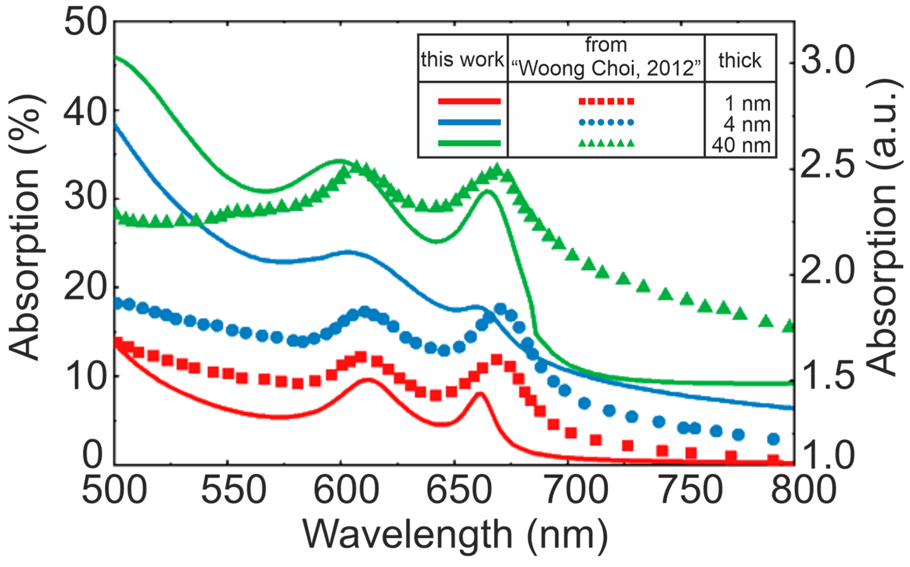
3.1. Optical Radiation Modeling
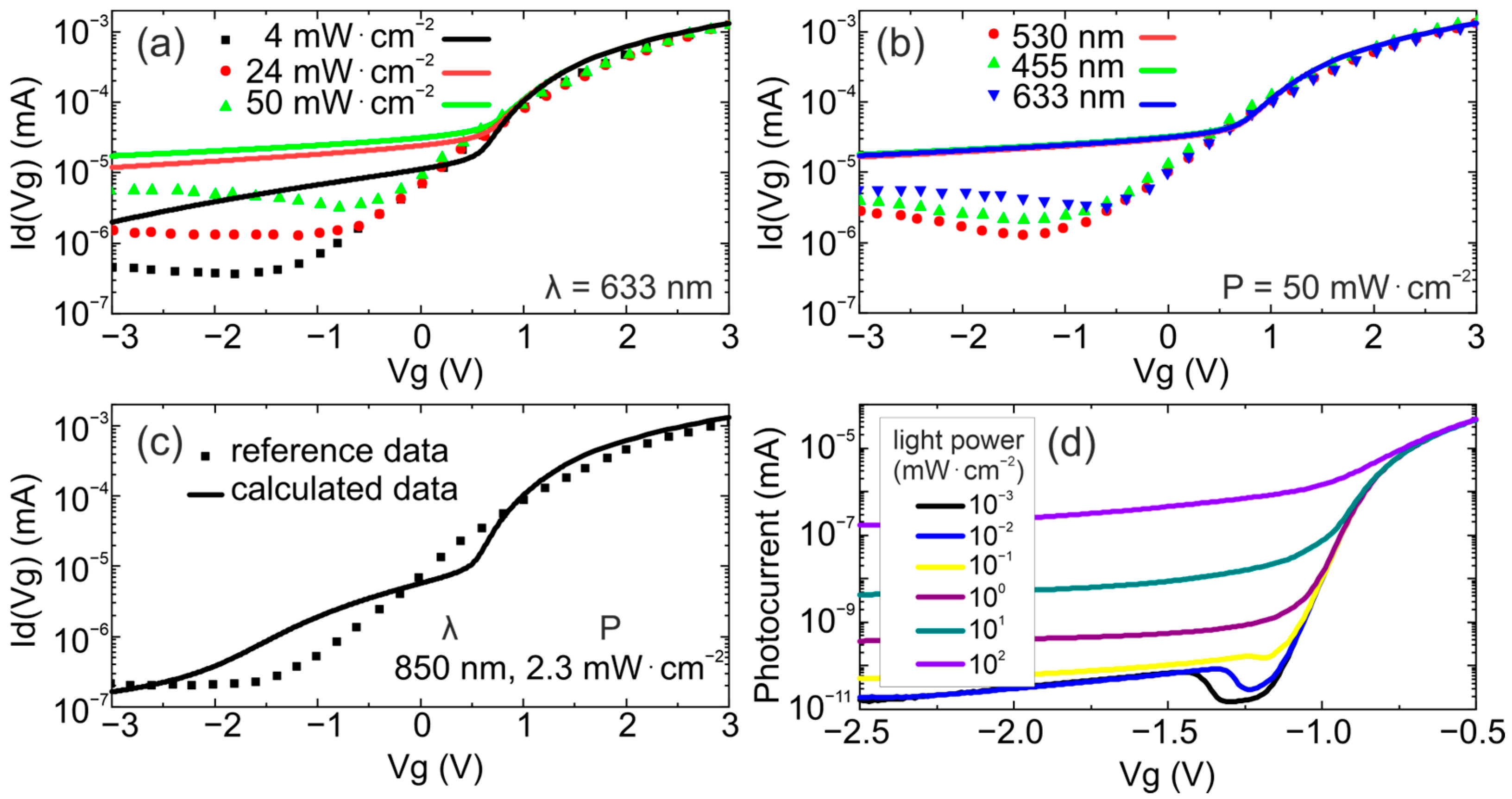
3.2. Dark Current Modeling
3.3. Photocurrent Modeling
4. Conclusions
Supplementary Materials
Author Contributions
Funding
Data Availability Statement
Conflicts of Interest
References
- Cao, L. Two-dimensional transition-metal dichalcogenide materials: Toward an age of atomic-scale photonics. MRS Bull. 2015, 40, 592–599. [Google Scholar] [CrossRef]
- Upadhyay, S.N.; Satrughna, J.A.K.; Pakhira, S. Recent advancements of two-dimensional transition metal dichalcogenides and their applications in electrocatalysis and energy storage. Emergent Mater. 2021, 4, 951–970. [Google Scholar] [CrossRef]
- Mir, S.H.; Yadav, V.K.; Singh, J.K. Recent advances in the carrier mobility of two-dimensional materials: A theoretical perspective. ACS Omega 2020, 5, 14203–14211. [Google Scholar] [CrossRef]
- Zhang, S.-R.; Batool, S.; Han, S.-T.; Zhou, Y.; Idrees, M. Novel charm of 2D materials engineering in memristor: When electronics encounter layered morphology. Nanoscale Horiz. 2022, 7, 480–507. [Google Scholar] [CrossRef]
- Papadakis, R.; Liu, J.; Jafri, S.H.M.; Zheng, X.; Zhao, M.; Hao, Y.; Zhang, C.; Zhai, R.; Liu, B.; Liu, W.; et al. Advances in two-dimensional materials for optoelectronics applications. Crystals 2022, 12, 1087. [Google Scholar] [CrossRef]
- Qumar, U.; Kaner, N.T.; Cassinese, A.; Babar, Z.U.D.; Hassan, J.Z.; Raza, A. 2D material-based sensing devices: An update. J. Mater. Chem. A 2023, 11, 6016–6063. [Google Scholar] [CrossRef]
- Kuc, A.; Heine, T.; Kis, A. Electronic properties of transition-metal dichalcogenides. MRS Bull. 2015, 40, 577–584. [Google Scholar] [CrossRef]
- Dias, A.C.; Fu, J.; Qu, F.; Azevedo, D.L. Band structure of monolayer transition-metal dichalcogenides and topological properties of their nanoribbons: Next-nearest-neighbor hopping. Phys. Rev. B 2018, 98, 075202. [Google Scholar] [CrossRef]
- Liu, Z.; Li, Y.; Peng, X.; Qiu, Y.; Liu, A.; Jiang, H.; Deng, T.; Guo, H.; Qin, Y.; Li, Y.; et al. The roadmap of 2D materials and devices toward chips. Nano-Micro Lett. 2024, 16, 119. [Google Scholar] [CrossRef]
- Yao, Z.; Jannat, A.; Zhong, L.; Ou, J.Z.; Haidry, A.A.; Zavabeti, A. Two-dimensional materials in large-areas: Synthesis, properties and applications. Nano-Micro Lett. 2020, 12, 66. [Google Scholar] [CrossRef]
- Nalwa, H.S. A review of molybdenum disulfide (MoS2) based photodetectors: From ultra-broadband, self-powered to flexible devices. RSC Adv. 2020, 10, 30529–30602. [Google Scholar] [CrossRef]
- Liu, J.; Guo, Z.; Chang, Z.; Li, J.; Guo, Y. Engineering plasmonic environments for 2D materials and 2D-based photodetectors. Molecules 2022, 27, 2807. [Google Scholar] [CrossRef]
- Stepanov, M.A.; Mishina, E.D.; Abdullaev, D.A.; Lavrov, S.D.; Guskov, A.A.; Galiev, R.R.; Shahurin, E.S. MoS2-based polarization-sensitive photodetectors with asymmetric plasmonic structures and decreased detection time. Opt. Mater. 2024, 152, 115452. [Google Scholar] [CrossRef]
- Chen, D.; Takahara, J. Absorption Enhancement of Excitons in WS2 by Silicon Huygens’ Metasurface. In JSAP-Optica Joint Symposia; Optica Publishing Group: Washington, DC, USA, 2024. [Google Scholar] [CrossRef]
- Xu, X.; Li, Z.; Wang, J.; Tao, L.; Xu, J.; Chen, Z. Enhancing light-matter interaction in 2D materials by optical micro/nano architectures for high-performance optoelectronic devices. InfoMat 2021, 3, 36–60. [Google Scholar] [CrossRef]
- Zhao, Z.; Rakheja, S.; Zhu, W.; Shukla, A.; Tunga, A. Physics-based modeling and validation of 2-D Schottky barrier field-effect transistors. IEEE Trans. Electron Devices 2023, 70, 2034–2041. [Google Scholar] [CrossRef]
- Stradi, D.; Stokbro, K.; Jacobsen, K.W.; Jelver, L. Schottky barrier lowering due to interface states in 2D heterophase devices. Nanoscale Adv. 2021, 3, 567–574. [Google Scholar] [CrossRef]
- Kim, N.Y.; Yang, H.; He, Z. Device simulation study of multilayer MoS2 Schottky barrier field-effect transistors. Nanotechnology 2024, 36, 035701. [Google Scholar] [CrossRef]
- Menyuk, C.R.; Islam, R.; Anjum, I.M.; Simsek, E. Study of an MoS2 phototransistor using a compact numerical method enabling detailed analysis of 2D material phototransistors. Sci. Rep. 2024, 14, 15269. [Google Scholar] [CrossRef]
- Kim, S.; Joo, J.; Choi, W.; Hong, S.C.; Cho, M.Y.; Kim, J.; Lee, J.H.; Jena, D.; Konar, A.; Cha, G.; et al. High-detectivity multilayer MoS2 phototransistors with spectral response from ultraviolet to infrared. Adv. Mater. 2012, 24, 5832–5836. [Google Scholar] [CrossRef]
- Dirè, S.; Pancheri, L.; Taffelli, A.; Quaranta, A. MoS2 based photodetectors: A review. Sensors 2021, 21, 2758. [Google Scholar] [CrossRef] [PubMed]
- Le, C.T.; Ky, D.L.C.; Khac, B.-C.T.; Kim, Y.S.; Chung, K.-H. Friction characteristics of mechanically exfoliated and CVD-grown single-layer MoS2. Friction 2018, 6, 395–406. [Google Scholar] [CrossRef]
- Chen, X.; Wang, R.; Song, B.; Jiang, H.; Zhai, T.; Gu, H.; Fang, M.; Ho, Y.; Liu, S. Layer-dependent dielectric function of wafer-scale 2D MoS2. Adv. Opt. Mater. 2019, 7, 1801250. [Google Scholar] [CrossRef]
- Handbook Series on Semiconductor Parameters; Levinshtein, M.S.Y.P.M., Ed.; World Scientific: Singapore, 1997; Volume 1. [Google Scholar]
- Brendel, R.; Bothe, K.; Schirmacher, A.; Kröger, I.; Lim, S.; Schinke, C.; Winter, S.; Nguyen, H.T.; Schmidt, J.; Vogt, M.R.; et al. Uncertainty analysis for the coefficient of band-to-band absorption of crystalline silicon. AIP Adv. 2015, 5, 067168. [Google Scholar] [CrossRef]
- Zwiller, V.; Steele, G.A.; Barkelid, M.; Buscema, M.; van der Zant, H.S.J.; Castellanos-Gomez, A. Large and tunable photothermoelectric effect in single-layer MoS2. Nano Lett. 2013, 13, 358–363. [Google Scholar] [CrossRef]
- Pospischil, A.; Furchi, M.M.; Mueller, T.; Polyushkin, D.K. Mechanisms of photoconductivity in atomically thin MoS2. Nano Lett. 2014, 14, 6165–6170. [Google Scholar] [CrossRef]
- Guskov, A.A.; Lavrov, S.D.; Bezvikonnyi, N.V. Kretschmann configuration as a method to enhance optical absorption in two-dimensional graphene-like semiconductors. Russ. Technol. J. 2024, 12, 96–105. [Google Scholar] [CrossRef]
- Wan, Y.; Dai, L.; Ma, Y.; Xie, Z.; Wang, W.; Rong, X.; Zhang, H. Measuring the refractive index of highly crystalline monolayer MoS2 with high confidence. Sci. Rep. 2015, 5, 8440. [Google Scholar] [CrossRef]
- Lin, M.-W.; Kravchenko, I.; Fowlkes, J.; Li, X.; Puretzky, A.A.; Rouleau, C.M.; Geohegan, D.; Xiao, K. Thickness-dependent charge transport in few-layer MoS2 field-effect transistors. Nanotechnology 2016, 27, 165203. [Google Scholar] [CrossRef]
- Romano, P.; Sessa, A.; Durante, O.; Sleziona, S.; Di Bartolomeo, A.; Giubileo, F.; Schleberger, M.; Martucciello, N.; Kumar, A.; Faella, E.; et al. Temperature-dependent photoconductivity in two-dimensional MoS2 transistors. Mater. Today Nano 2023, 24, 100382. [Google Scholar] [CrossRef]
- Chang, W.-H.; Hsieh, S.-H.; Li, K.-S.; Yang, S.-T.; Hou, T.-H.; Lu, C.-I.; Lin, C.-P.; Lu, T.-H.; Chen, J.-H.; Chen, C.-H.; et al. Defect-engineered room temperature negative differential resistance in monolayer MoS2 transistors. Nanoscale Horiz. 2022, 7, 1533–1539. [Google Scholar] [CrossRef]
- Sreelakshmi, B.; Thamankar, R. Investigation of the transient photo-response and switching window of an Al/indigo/Al device: Unveiling negative photoconductivity and the photo-enhanced memory window. Mater. Adv. 2024, 5, 5912–5921. [Google Scholar] [CrossRef]
- Terabe, K.; Takagi, S.; Toprasertpong, K.; Takenaka, M.; Tsuchiya, T.; Nur, R. A floating gate negative capacitance MoS2 phototransistor with high photosensitivity. Nanoscale 2022, 14, 2013–2022. [Google Scholar] [CrossRef]
- Zubair, A.; Nourbakhsh, A.; Dresselhaus, M.S.; Palacios, T. Transport Properties of a MoS2/WSe2 Heterojunction Transistor and Its Potential for Application. Nano Lett. 2016, 16, 1359–1366. [Google Scholar] [CrossRef]
- Laturia, A.; Van De Put, M.L.; Vandenberghe, W. Dielectric properties of hexagonal boron nitride and transition metal dichalcogenides: From monolayer to bulk. Npj 2D Mater. Appl. 2018, 2, 6. [Google Scholar] [CrossRef]
- Chernozatonskii, L.A.; Artyukh, A.A. Quasi-two-dimensional transition metal dichalcogenides: Structure, synthesis, properties, and applications. Phys.-Uspekhi 2018, 61, 2–28. [Google Scholar] [CrossRef]
- Gerardot, B.D.; Krauss, T.F.; Sapienza, R.; Tartakovskii, A.I.; Vezzoli, S.; Huq, T.; Louca, C.; Hu, X.; Sortino, L.; Randerson, S.; et al. Van der Waals Materials for Applications in Nanophotonics. Laser Photon Rev. 2023, 17, 2200957. [Google Scholar] [CrossRef]


| Parameter | Value | Unit | Reference |
|---|---|---|---|
| MoS2 parameters | |||
| Band gap | 1.3 for bulk and 1.8 for 1 nm | eV | [18] |
| Electron affinity | 4.0 for bulk and 4.7 for 1 nm | eV | |
| Effective density of states, valence and conduction band | 8.87 × 10¹⁸ | cm−3 | |
| Electron mobility | 2.5–65 | cm2V−1s−1 | |
| Electron–hole lifetime | 0.1–1 | ns | |
| Donor concentration | 5 × 10¹⁷ | cm−3 | |
| Relative permittivity | 11 for bulk and 4.2 for 1 nm | 1 | |
| Barrier height | 100 | meV | |
| Refractive index | Function from wavelength | 1 | [23] |
| Silicon parameters | |||
| Band gap | 1.12 | eV | [24] |
| Electron affinity | 4.05 | eV | |
| Effective density of states, valence band | 1.04 × 10¹⁹ | cm−3 | |
| Effective density of states, conduction band | 1.28 × 10¹⁹ | cm−3 | |
| Electron mobility | 1450 | cm2V−1s−1 | |
| Hole mobility | 500 | cm2V−1s−1 | |
| Refractive index | Function from wavelength | 1 | [25] |
| Acceptor concentration | 1019 | cm−3 | |
| Geometry parameters | |||
| Channel length | 3 | µm | [20] |
| Channel width | 7 | µm | |
| Oxide thickness | 50 | nm | |
| Silicon thickness | 500 | nm | |
| Schottky region | 50 | nm | |
| PML thickness | 1000 | nm | |
| Air thickness | 1000 | nm | |
Disclaimer/Publisher’s Note: The statements, opinions and data contained in all publications are solely those of the individual author(s) and contributor(s) and not of MDPI and/or the editor(s). MDPI and/or the editor(s) disclaim responsibility for any injury to people or property resulting from any ideas, methods, instructions or products referred to in the content. |
© 2025 by the authors. Licensee MDPI, Basel, Switzerland. This article is an open access article distributed under the terms and conditions of the Creative Commons Attribution (CC BY) license (https://creativecommons.org/licenses/by/4.0/).
Share and Cite
Lavrov, S.D.; Guskov, A.A. Modeling of Phototransistors Based on Quasi-Two-Dimensional Transition Metal Dichalcogenides. Modelling 2025, 6, 47. https://doi.org/10.3390/modelling6020047
Lavrov SD, Guskov AA. Modeling of Phototransistors Based on Quasi-Two-Dimensional Transition Metal Dichalcogenides. Modelling. 2025; 6(2):47. https://doi.org/10.3390/modelling6020047
Chicago/Turabian StyleLavrov, Sergey D., and Andrey A. Guskov. 2025. "Modeling of Phototransistors Based on Quasi-Two-Dimensional Transition Metal Dichalcogenides" Modelling 6, no. 2: 47. https://doi.org/10.3390/modelling6020047
APA StyleLavrov, S. D., & Guskov, A. A. (2025). Modeling of Phototransistors Based on Quasi-Two-Dimensional Transition Metal Dichalcogenides. Modelling, 6(2), 47. https://doi.org/10.3390/modelling6020047