1. Introduction
Power converters are indispensable in electrical platforms and systems such as electric vehicles [
1], portable electronic devices [
2], and computing systems [
3]. The recent and future trend is to maximize the integration level of switching power converters to yield several advantages such as smaller size, lighter weight, and the integration of these converters with their loads on the same chip for reduced distribution delays (faster dynamic response) and reduced distribution losses. To achieve high-density power conversion, one of the most difficult challenges relates to the ability to integrate a magnetic component such as a power inductor, which is by far the largest component in a power converter. Power inductor integration is critical to achieving System on Chip (SoC) [
4] and System in Package (SiP) [
5]. Integrated magnetics is a low-level integration, which combines several magnetic components, such as inductors and transformers, of a converter into a single magnetic structure [
6]. The on-chip integration of a power inductor, aiming to achieve high saturation current in a small size (footprint) and a sufficient inductance value, is an essential building block for high-density power conversion.
Inductance and saturation current values are functions of several design parameters such as ferrite core permeability, the number of turns of copper winding, and the ferrite core’s thickness and footprint. A tradeoff between different design parameters needs to be considered when designing power inductors. On-chip integrated power inductors with magnetic cores yield higher inductance values but at the expense of a limited saturation current (usually less than 1 A) [
7]. Many common ferrite magnetic core materials have limited saturation flux densities, say 0.3–0.5 T, which limits the amount of flux the winding of the inductor can generate before the core is saturated, which in turn limits the power inductor saturation current.
In order to achieve a high saturation current and at the same time maintain a high inductance value for power inductors, the magnetic core size needs to be increased, or magnetic core materials with high saturation magnetization have to be employed. However, increasing the core size will significantly increase the size of the power inductor and makes it harder to integrate. Meanwhile, magnetic materials with high magnetization, such as permalloy [
8], usually have relatively low resistivity, leading to high eddy current loss in the inductor core. Permanent magnet (PM) materials have been used to increase the saturation current for power inductors with different core structures. In [
9], a PM was utilized in a toroid power inductor to increase its saturation current while keeping the inductor size and inductance value unchanged. Different distribution schemes for utilizing PM in a toroid power inductor were evaluated and studied using a 3D physical model in [
10]. The utilization of PM material for increasing saturation current was also evaluated in an EE-core power inductor [
11].
Planar power inductors have been presented and studied in the literature. Related studies have mainly focused on modeling and fabrication. In relation to modeling, in [
12], the effect of utilizing magnetic substrates with planar inductors was modeled, and an expression of the enhancement in the inductance due to magnetic substrates was obtained. In [
13], the effect of sandwiching a spiral planar inductor between two magnetic substrates was analyzed using the method of current images, and expressions were obtained for magnetic fields and inductance. Inductance expressions for different planar inductor geometries (square, hexagonal, octagonal, and circular) have been presented in [
14]. In [
15], the authors presented different planar inductor geometries with their models and performance evaluation for sensing applications. A physics-based model for a spiral planar inductor was presented in [
16], taking the capacitance between adjacent turns, self-inductance, and substrate capacitance into consideration. In [
17], the authors presented an analytical calculation method to estimate the self-inductance of planar coils without geometry limitations. A 3D physical model was utilized to optimize the number of copper winding turns for a planar power inductor in [
18]. The authors in [
19] presented an analysis and optimization tool for spiral planar inductors operated at high frequency, with the capability of determining the inductance and electrical parameters for different planar inductor geometries (e.g., octagonal and hexagonal). An electrical circuit model for a graphene-based on-chip power inductor was introduced in [
20]. In relation to fabrication, a planar inductor with NiZn ferrite layers was fabricated using a screen printing method in [
21], while, in [
22], a planar inductor with a MnZn ferrite layer was presented. A planar inductor with an FeSiCr-based core was introduced in [
23]. Planar power inductors can also be embedded into a silicon substrate as in [
24], or within printed circuit boards (PCB) as presented in [
25,
26].
This paper presents a 3D physical model and a magnetic circuit model for an on-chip planar power inductor design that utilizes a permanent magnet to double the saturation current. The presented power inductor is named the permanent magnet on-chip power inductor (PMOI). The power inductor without PM is referred to as OPI in this paper.
The remainder of this paper is organized as follows.
Section 2 describes the PMOI structure and its operation principle. In
Section 3, magnetic circuit modeling for the OPI and PMOI is presented. In
Section 4, a 3D physical model for PMOI for an exemplary design is built using ANSYS
®/Maxwell
® software package, and simulation results are then presented and discussed for the 3D physical model. The conclusion is given in
Section 5.
2. PMOI Structure and Operation Principle
The winding of the power inductor produces flux, which results in flux density (Bwind) that is directly proportional to the DC current passing through it. The magnetic core of the power inductor saturates at a maximum flux density (Bsat). For example, this Bsat value can be 0.46 T for a ferrite core.
This
Bsat value limits the maximum current of the power inductor before saturation (
Isat). The relationship between
Isat and
Bsat can be described as in (1).
where
N is the number of winding turns,
A is the cross-section area of the winding, and
L is the inductance. However, if a material that generates an opposing flux (
Bopp) to the flux generated by the winding
Bwind is utilized in the power inductor structure, the saturation current could be increased. In this paper, the material that generates
Bopp is a PM material.
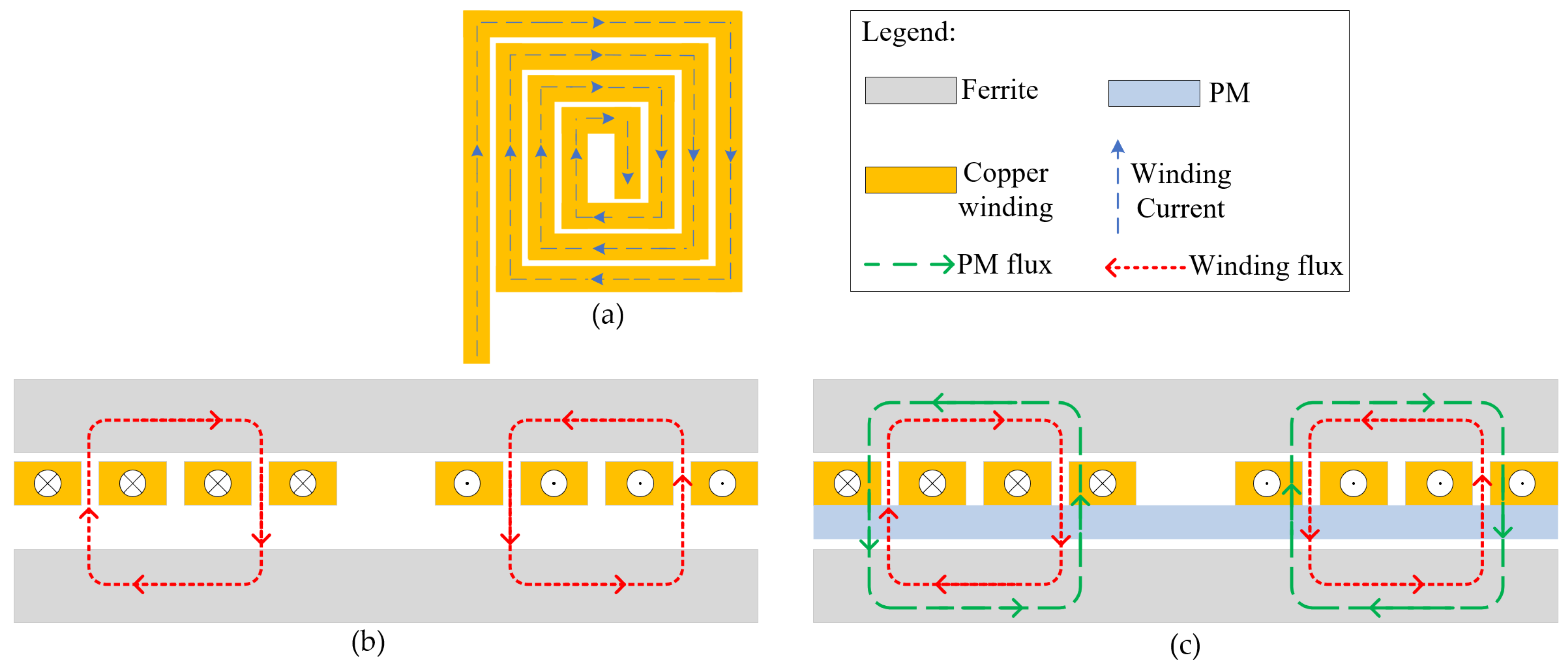
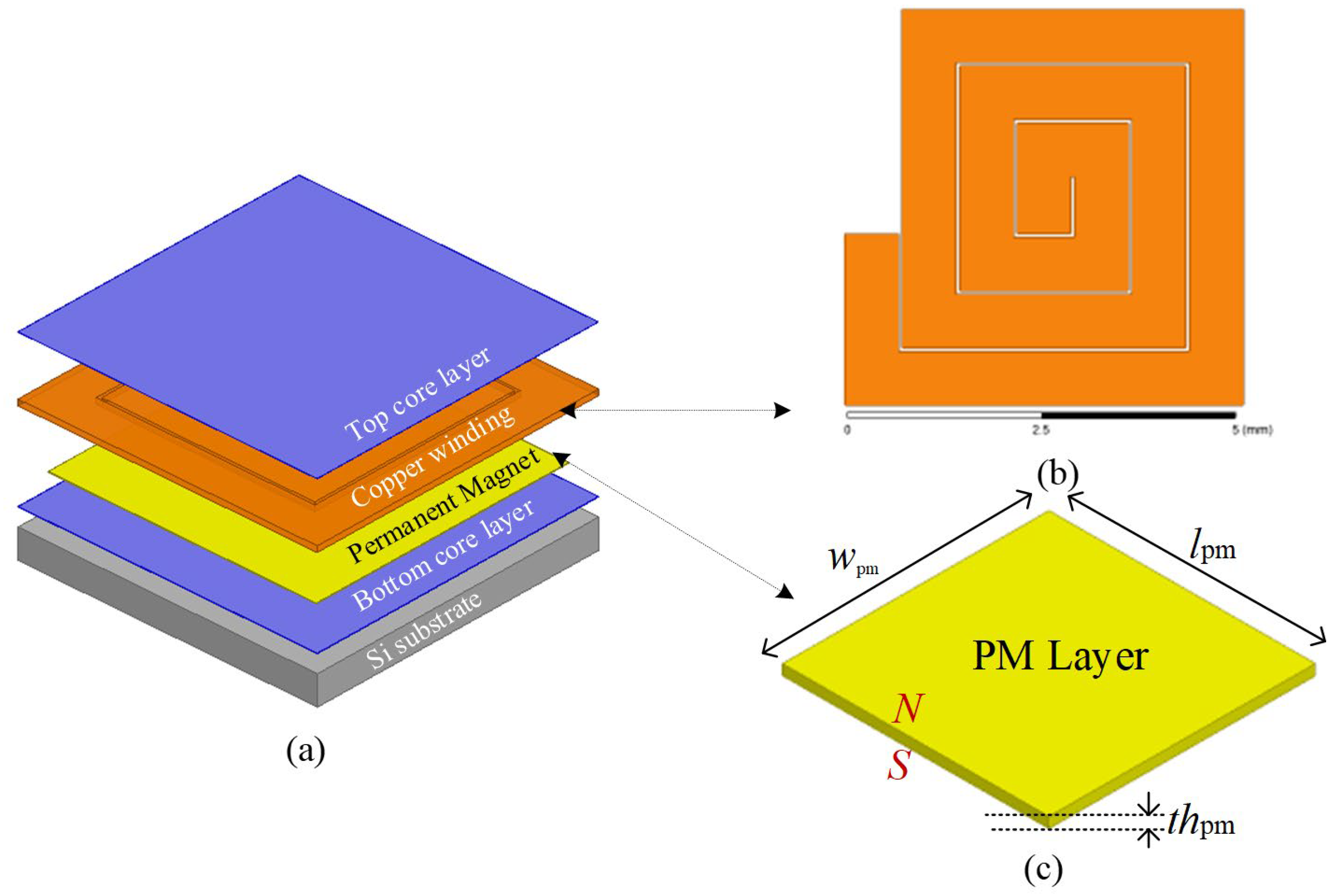
Figure 1 shows an example spiral power inductor for on-chip integration with and without a PM layer. In
Figure 1a, the power inductor on a silicon (Si) substrate (other substrate types could also be used) consists of a spiral winding between two ferrite core layers (e.g., NiZnCu ferrite [
21]). There is a gap (acting as an air gap) between the winding and each ferrite layer. The gaps are filled with insulating material such as SiO
2. In
Figure 1b, an additional PM layer is placed in part of the gap between the bottom ferrite layer and the winding (the total thickness of the power inductor is kept the same in both cases). The
Bopp generated by the PM opposes the
Bwind of the winding (they partially or completely cancel each other out).
Assuming that the power inductor (OPI) of
Figure 1a has a saturation current of
Isat-OPI. The saturation current of the inductor (PMOI) in
Figure 1b can potentially be double that for
Figure 1a (
Isat-PMOI = 2 ×
Isat-OPI) by using the following scheme: The type and layer thickness of the PM are developed such that
Bopp = −
Bsat. This way, the core will start with flux that is equal to the saturation flux density at zero current, and this flux will first decrease to zero when the current is equal to
Isat-OPI and then it will increase to the saturation flux density when the current is equal to 2 ×
Isat-OPI. To illustrate this concept,
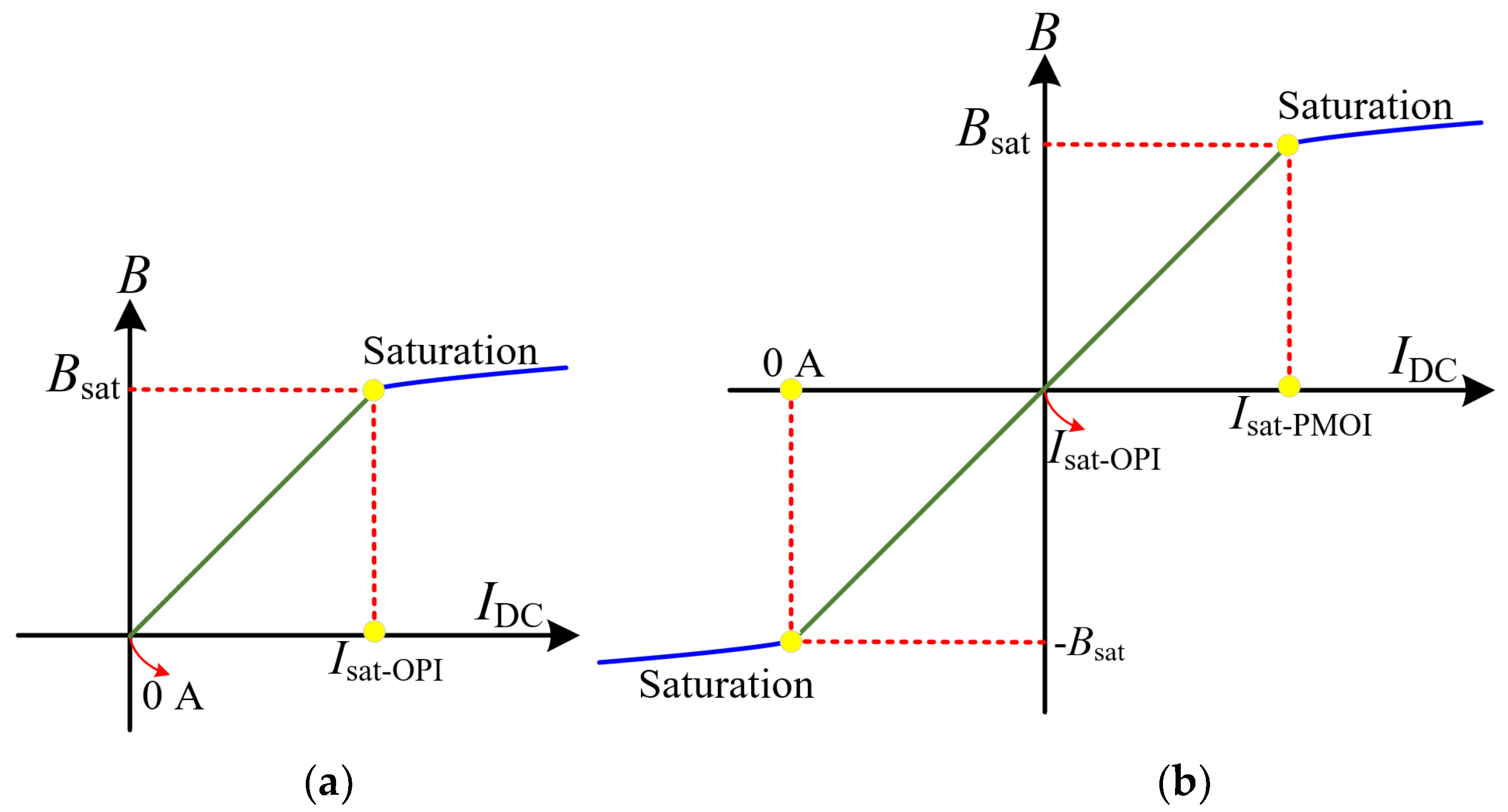
Figure 2 shows the relation between the applied DC current
IDC and the magnetic flux density
B for both the OPI and PMOI. For the OPI, at
IDC = 0, the magnetic flux density
BOPI = 0. Meanwhile, at
IDC = 0, the magnetic flux density for the PMOI
BPMOI = −
Bsat due to the flux generated by the PM. As the applied current
IDC increases, the magnetic flux density for the OPI increases until it reaches
BOPI =
Bsat when
IDC=
Isat-OPI, as shown in
Figure 2a. At this point, the OPI starts to saturate, and the inductance value starts to decrease. For the PMOI, as the applied current
IDC increases, the magnetic flux density
BPMOI decreases until it becomes equal to zero when
IDC =
Isat-OPI, as shown in
Figure 2b. At this point, the flux generated by the winding is equal in magnitude and opposite in direction to the flux generated by the PM (net magnetic flux density is equal to zero). When
IDC = 2 ×
Isat-OPI, the net magnetic flux density
BPMOI =
Bsat and the core of the PMOI start to saturate.
3. Magnetic Circuit Modeling of OPI and PMOI
Figure 3 illustrates the magnetic flux lines for both OPI and PMOI. In
Figure 3a, the magnetic flux due to the winding current is illustrated. As explained earlier, when utilizing a PM in one of the air gaps (the bottom air gap in this paper), another flux can be generated to oppose the winding flux, as shown in
Figure 3b. As shown, the flux of the PM opposes the flux due to the current; therefore, the net flux in the ferrite core is reduced. As a result, the saturation current is increased.
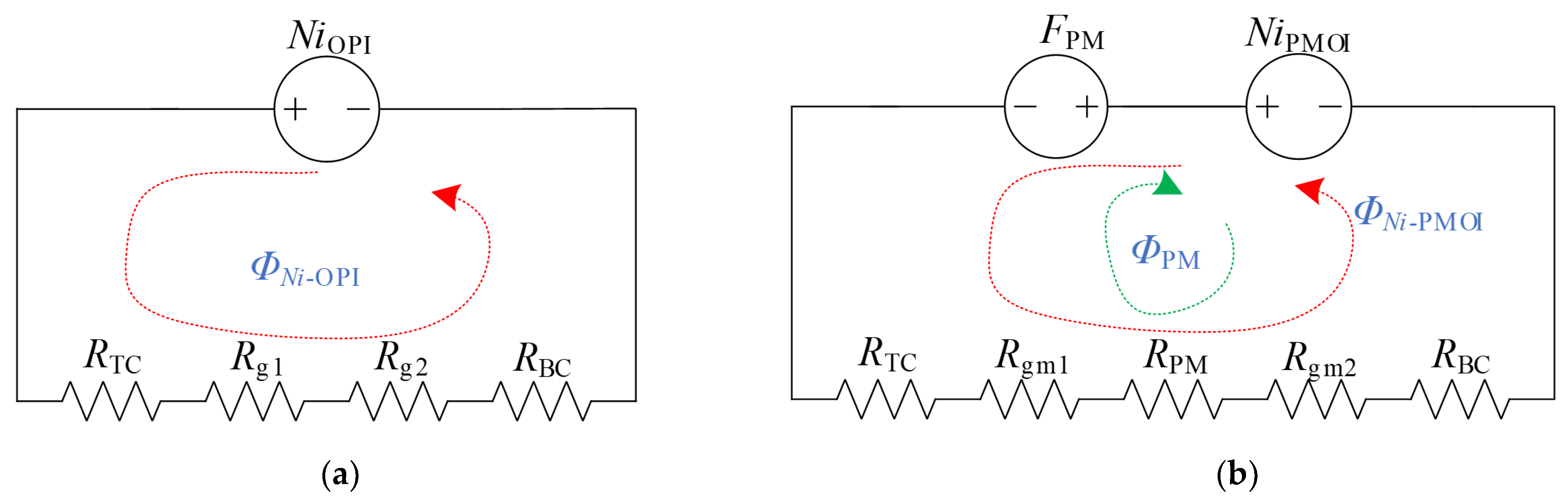
Magnetic circuit models for OPI and PMOI are shown in
Figure 4, where
FPM is the magnetomotive force of the PM,
i is the current flowing in the windings,
ΦNi is the winding flux, and
ΦPM is the PM flux. The reluctance
R for each layer in the inductor structure is as follows: top ferrite core reluctance
RTC, bottom ferrite core reluctance
RBC, top air gap reluctance
Rg1 for the OPI, bottom air gap reluctance
Rg2 for the OPI, top air gap reluctance
Rgm1 for the PMOI, bottom air gap reluctance
Rgm2 for the PMOI, and the permanent magnet reluctance
RPM. The leakage inductance and fringing effect are not taken into consideration. Using the magnetic circuit models shown in
Figure 4, (2) and (3) can be obtained for OPI and PMOI, respectively, by applying Kirchhoff’s voltage law (KVL). Since the bottom ferrite core and top ferrite core are identical, their reluctances can be combined into
RC, where
RC = 2
RBC = 2
RTC.
The reluctance of the power inductor is expressed in (4), where
lm is the magnetic path length,
µo is the vacuum permeability,
µr is the relative permeability, and
Ac is the cross-section area of the ferrite core.
Since the PM’s relative permeability is almost equal to 1 [
27], the PM effectively acts as an air gap. Therefore, both the OPI and PMOI have almost an equal value for the total air gap reluctance, i.e.,
Based on (5), (2) and (3) can be rewritten as
The ferrite core total flux is
Φ =
B.
Ac. To express the saturation current
Isat for both the OPI and the PMOI, (6) and (7) can be rewritten by replacing
I by
Isat and
Φ by
Bsat.
Ac. This yields (8) and (9).
It can be noted from (8) and (9) that the saturation current of the PMOI (
Isat_PMOI) is higher than the saturation current of the OPI (
Isat_OPI) because of the PM’s magnetomotive force
FPM. This can be described as in (10), where
Ic is the current at which the PM fully cancels the flux due to the current in the winding and is equal to
FPM/
N. The higher the magnetomotive force of the PM, the larger the saturation current. However, in order to avoid saturating the ferrite core by the PM itself when the DC current is equal to 0 A, the magnetomotive force
FPM of the PM must satisfy the condition shown in (11).
Based on (10) and (11), as long as the ferrite core is not saturated by the PM, the saturation current of the PMOI can be twice the saturation current of the OPI, while both OPI and PMOI have the same inductance value.
Equation (9) can be rewritten as in (12). By solving for
, (13) can be obtained, where
H is the magnetic field strength and
is the PM thickness. By solving for
lm, (14) can be obtained. For example, if a PM is selected with
H = 1592 kA/m to increase the saturation current from 4 A to 8 A, the thickness of the PM should be ~7.5 μm (which is the value used in the design presented in the next section).
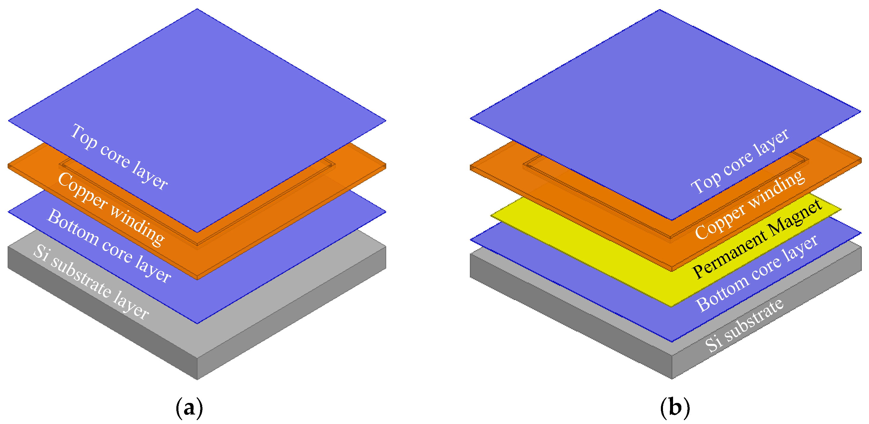
4. ANSYS®/Maxwell® 3D Modeling and Simulation of PMOI
Figure 5 shows a diagram of the example PMOI with more details compared to
Figure 1b. A rectangular spiral winding structure as shown in
Figure 5b is employed in the example PMOI architecture. The PM layer is vertically magnetized as illustrated in
Figure 5c, such that the north pole is on the top and the south pole on the bottom, or vice versa.
Finite element analysis (FEA) is performed to find numerical solutions for physics-based models in order gain insights into design and to predict performance [
28,
29,
30,
31,
32]. Simulation results for the 3D physical model are utilized to validate the magnetic circuit model presented in
Section 3. In this paper, the 3D physical model’s simulation results are obtained using the ANSYS
®/Maxwell
® model for an example on-chip power inductor design (as in
Figure 5), with two versions: the first version is without using PM (OPI) and the second version is with PM (PMOI). Both power inductors’ switching frequency of operation can be from 1 MHz to 10 MHz, but the results in this section are for 5 MHz.
Table 1 shows a summary of the design specifications for the two versions. In the 3D physical model of PMOI, the top and bottom core materials used are both NiZnCu ferrite (
Bsat = 0.46 T, relative permeability
μr = 120, and resistivity
ρ = 10
8 Ω) [
21]), and the PM material used is NdFeBN45SH (residual flux density
Br = 1.32 T, coercivity
Hc = 1003 kA/m and intrinsic coercivity
Hci = 1592 kA/m) [
27]. The copper relative permeability and conductivity are 0.999991 and 5.8 × 10
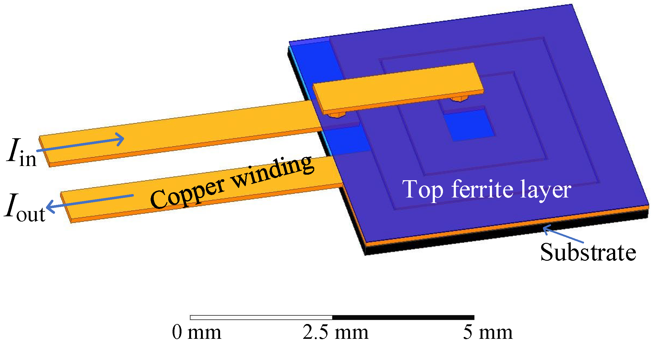
7 Siemens/m, respectively. The copper coil is excited by a DC current flowing through the winding, as indicated by the input current (
Iin) and output current (
Iout) in
Figure 6. The region surrounding the inductor is a vacuum with a permeability of
µo = 1.
Figure 6 shows an ANSYS
®/Maxwell
® 3D physical model of the designed PMOI according to the design specifications in
Table 1. Comparisons between the OPI and PMOI based on simulation results for the 3D physical model are summarized in
Table 2.
4.1. Simulation Results for OPI
The inductance of the OPI measured from ANSYS
®/Maxwell
® is 50.9 nH.
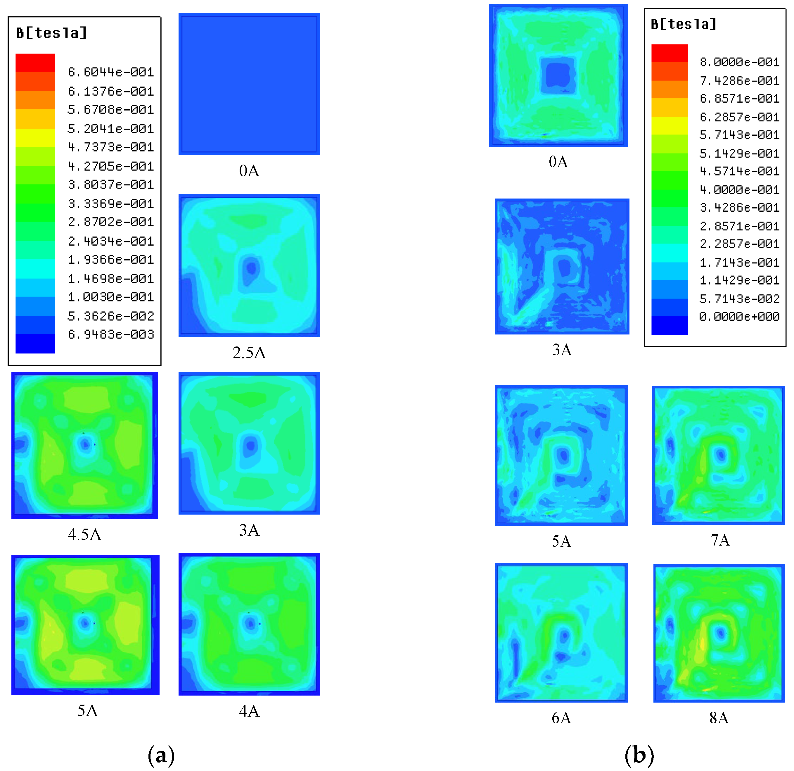
Figure 7a shows the
B field of the OPI under different input DC current values. For convenience of comparison, limited scaling is used in ANSYS
®/Maxwell
® when showing the calculated
B field of the ferrite layer for OPI and PMOI in
Figure 7a,b. Meanwhile, both the top and bottom ferrite layers are about to saturate at the same time, thus
Figure 7a,b only show the
B field of the bottom ferrite layer of OPI and PMOI. It can be observed from
Figure 7a that the ferrite core layer of the OPI is about to saturate when the DC input current is 4 A.
4.2. B Field of the PMOI
The inductance of the PMOI measured from ANSYS
®/Maxwell
® is 49.1 nH, which is close to the inductance value of the OPI (50.9 nH).
Figure 7b shows the
B field of PMOI ferrite core layers when the DC input current increases from zero to 8 A. When the input current is zero, the value of
B is less than the
Bsat (0.46 T) of both top and bottom ferrite core layers, which means the inductor is not saturated by PM itself. When the input DC current increases from 0 to 8 A, the
B value first decreases to approximately zero (when the input current is 3 A), and then increases from zero to a certain value. It can be observed from
Figure 7b that the core of PMOI starts saturating around 7.5 A. The 3D physical model’s simulation results for inductance values and saturation current values for both OPI and PMOI agree with the magnetic circuit model presented in
Section 3, showing that the saturation current of the PMOI can be twice the OPI’s saturation current when both have the same inductance value.
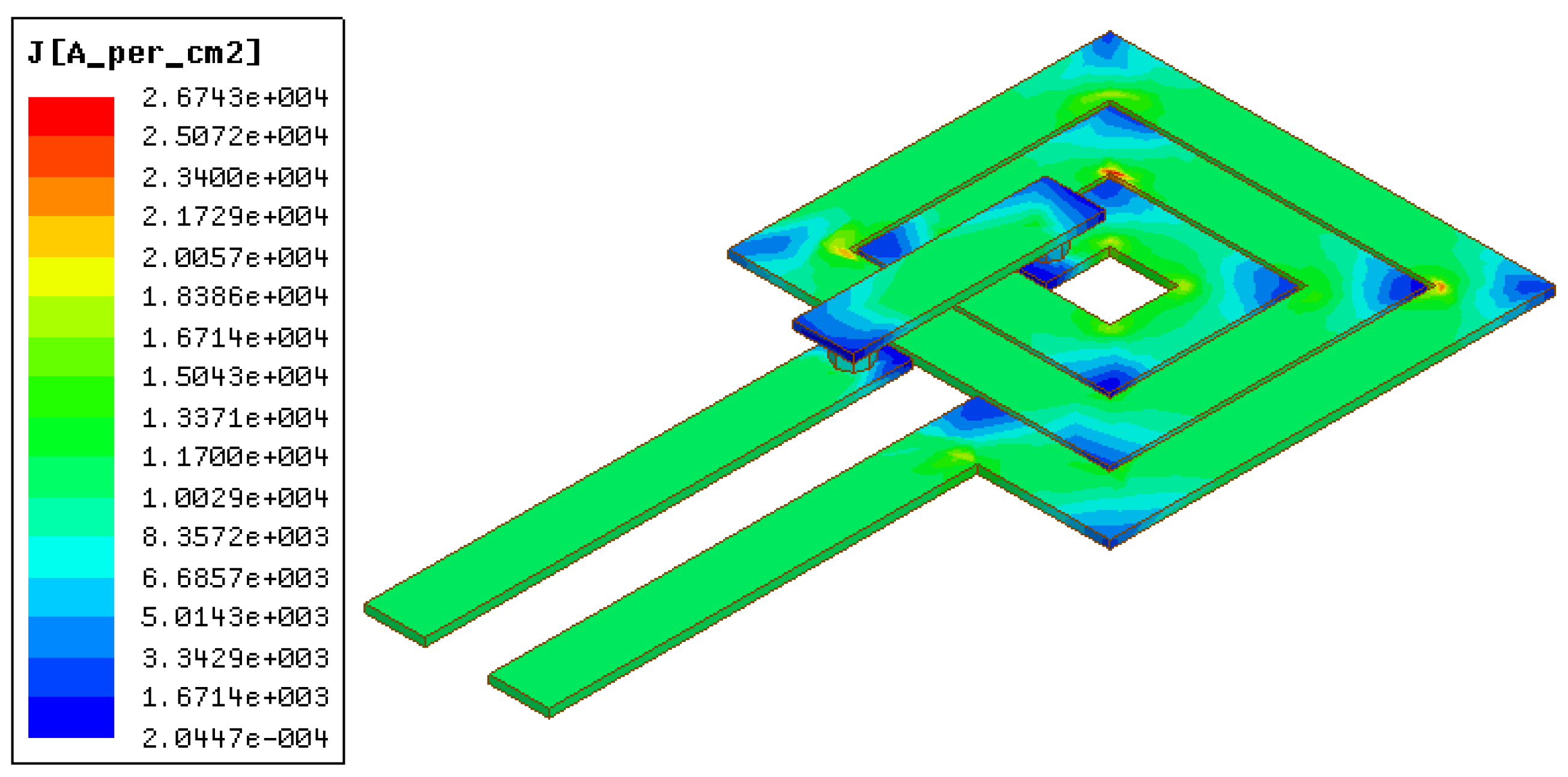
4.3. Current Density (J) of the PMOI
One of the constrains in a power inductor design is the current density
J of the windings.
Figure 8 shows the current density distribution of the PMOI when the DC input current is 7.5 A. In order to find the exact maximum
J value, auto scaling is used in ANSYS
®/Maxwell
®. It can be observed from
Figure 8 that the maximum
J value is 267.4 A/mm
2 [
33].
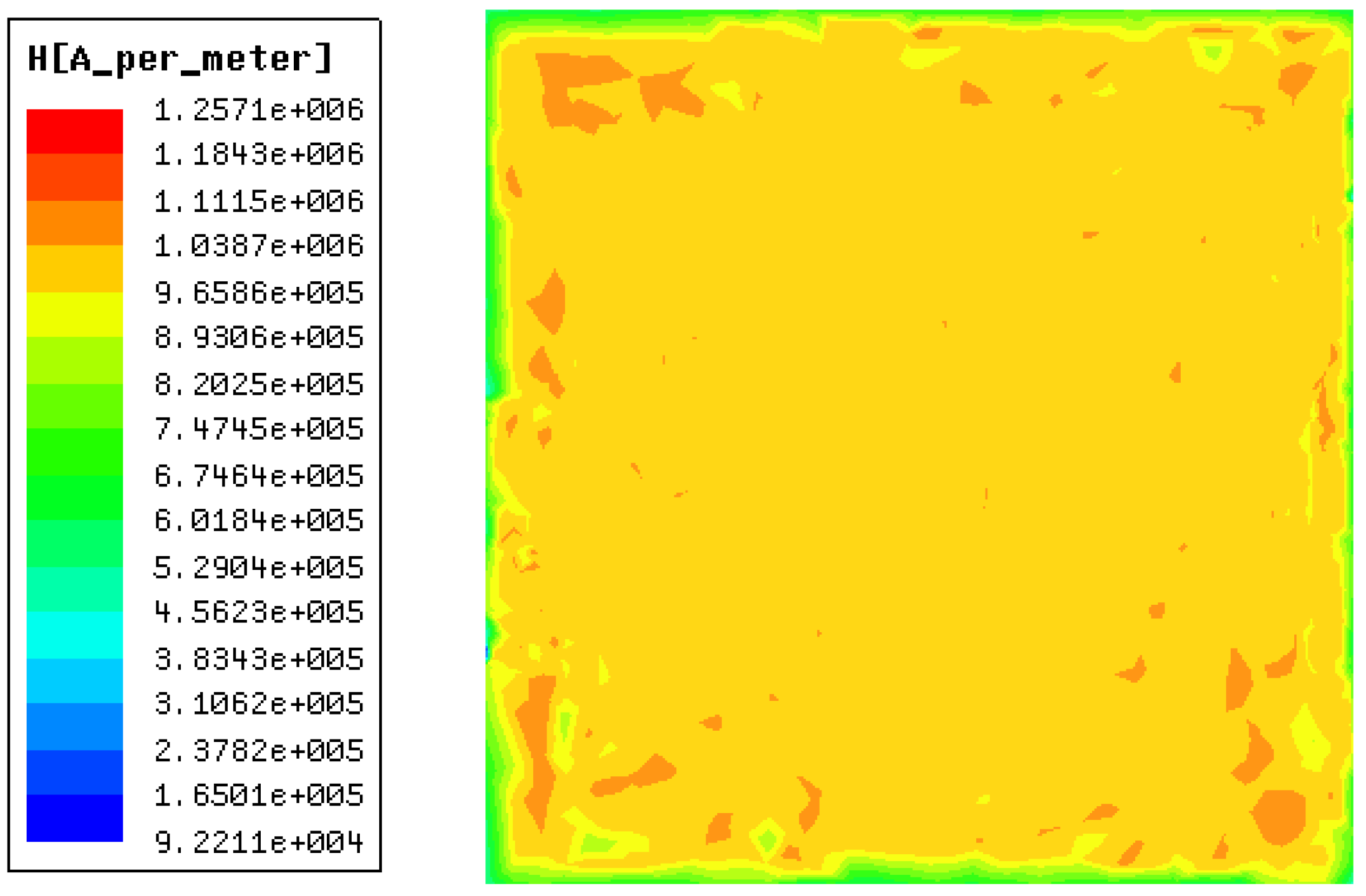
4.4. Demagnetization Problem
The demagnetization of the NdFeB-N45SH PM material occurs when a magnetic field
H larger than 12.97 × 10
5 A/m at 20 °C is applied in the direction of demagnetization [
27].
Figure 9 shows the
H field distribution in the PMOI when the DC input current is 10 A. It can be observed that the maximum
H value is less than 12.57 × 10
5 A/m, which means the PM used in this PMOI design will not be demagnetized even when the input current is as high as 10 A.
4.5. Results Discussion
The effect of the PM’s addition can be observed by comparing
Figure 7a,b. When the PM layer is used in a PMOI design, as shown in
Figure 7b, the net
B values in the top and bottom ferrite core layers decrease and then increase back to
Bsat, unlike the case in
Figure 7a without the PM, where the
B value continuously increases.
When the DC input current
IDC increases from zero to 8 A, the
B of PM remains constant (the value is shown in
Figure 7b, when
IDC = 0), since in this case there is no
B from the windings and the
B in the core is the
B of the PM, while the
B of windings increases as the current increases, leading to the net
B of the PMOI core first decreasing from the
B of PM to zero and then increasing from zero to
Bsat, as shown in
Figure 7b. When
IDC is less than 3 A, the
B of the PM is larger than the
B of the windings. In this case, the net
B has the same orientation as the
B of PM. When
IDC = 3 A, the net
B is approximately zero. The net
B distribution in the PMOI core when
IDC increases from 3 A to 7.5 A, as shown in
Figure 7b, is similar to the net
B distribution of the OPI when
IDC increases from zero to 4 A, as shown in
Figure 7a. It should be noted that in the PMOI core, the amount of flux generated by the PM is always there, and the winding flux is also there, but their net in the core is reduced as a result of cancelation, since the two fluxes are in opposite directions and the core saturation current is therefore increased.
The simulation results for the presented 3D physical models of OPI and PMOI are compared in
Table 2. It can be observed that, compared with the OPI design, the PMOI has the same inductance value, same total inductor volume, same winding number of turns, and same gap length, while the saturation current increases from 4 A to 7.5 A, which is nearly double.
The PM can be included as an additional layer in planar inductors during the fabrication process to increase the inductor saturation current. For example, taking the inductor design in [
22], if a PM layer is added between the Mn–Zn ferrite layer and the copper coil, the saturation current can be increased. Similarly, a PM layer can be added between the carbonyl-iron powder (CIP)/epoxy composite magnetic core and the copper coil to increase the saturation current for the planar power inductor presented in [
34].
Based on the advantages presented and discussed in the paper, a planar power inductor with PM offers a low-profile, high-power, and high-density solution for power converters used in applications such as telecommunications, computing platforms, and automotives.
5. Conclusions
This paper presents a 3D physical model and a magnetic circuit model to demonstrate and evaluate the advantages of adding a PM material to the integrated on-chip power inductor. The magnetic circuit model shows that adding a PM allows for doubling the saturation current of the inductor without affecting the inductance value. The simulation results for the 3D physical model agree with the magnetic circuit model, and show that the example PMOI increases the saturation current of the OPI from 4 A to 7.5 A with the same size and inductance value. With the above advantage, PMOI contributes to the reduction in size and weight, in addition to increasing the power density and integration level of the on-chip integrated power inductor. The PMOI has a potential consequence, which is the added cost as a result of the PM layer. However, this yields the advantage of doubling the saturation current without increasing the power inductor size or the cost of the material (e.g., core/ferrite), due to the size increase required to obtain a higher saturation current.
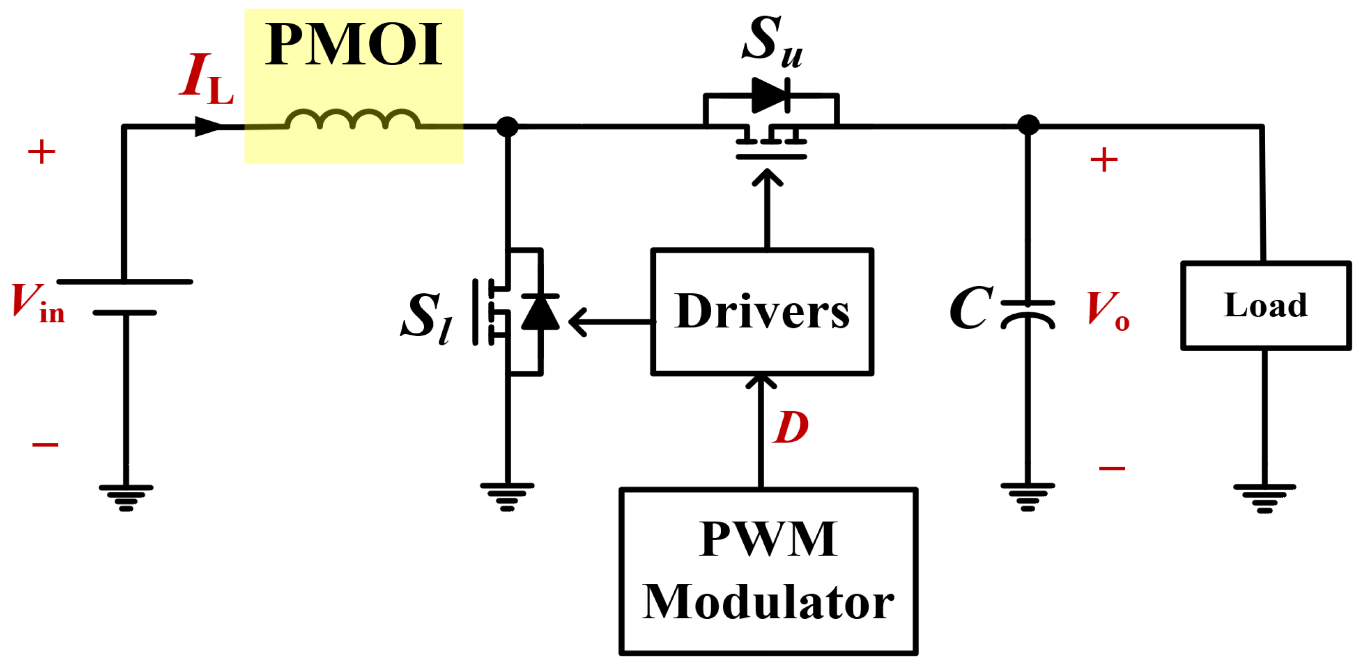
Future works will include evaluating the inductor core losses (eddy current loss and hysteresis loss), in addition to the fabrication and characterization of the PMOI and testing its operation in an experimental DC–DC power converter. For example, the presented PMOI can be tested and evaluated in a buck converter, as shown in
Figure 10. Experimental validation helps in evaluating the power inductor performance under operating conditions in a power converter.
The reliability of the PMOI design is likely to match the reliability of any similar planar power inductor design. However, future work can include further reliability evaluations and comparisons.


