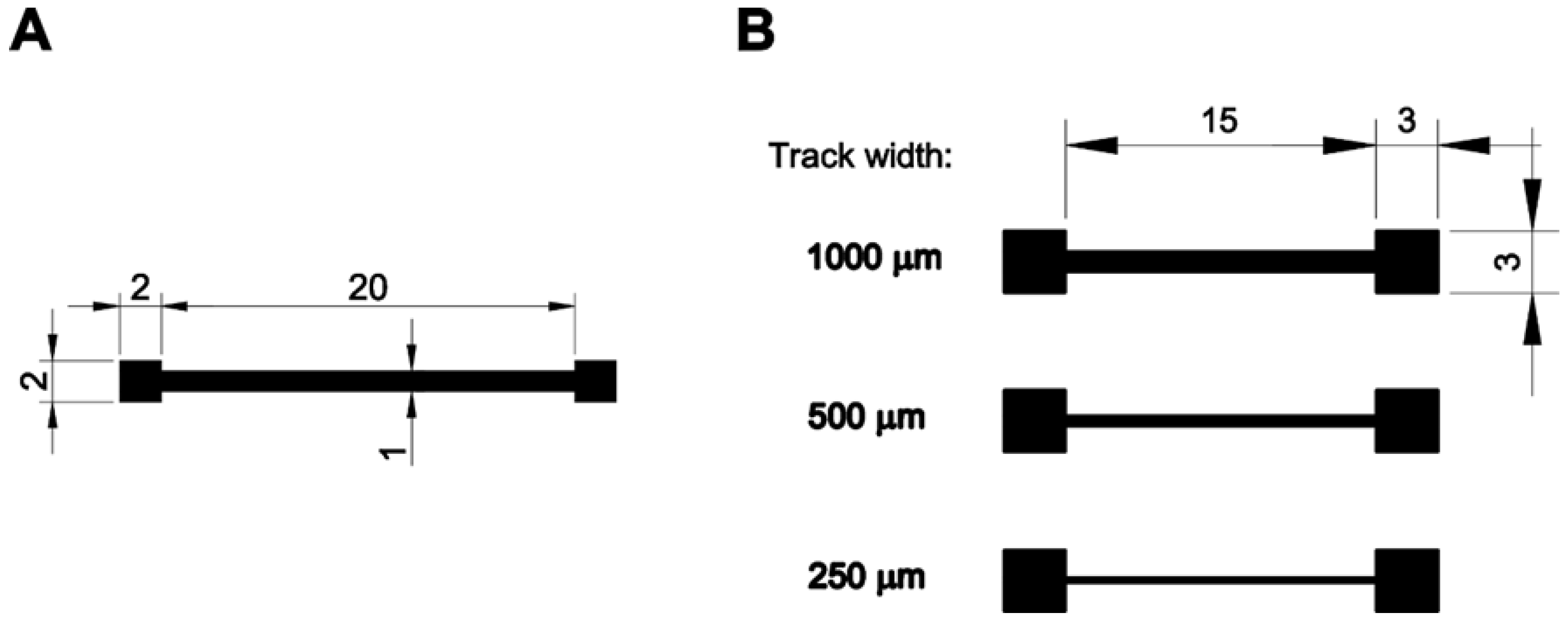
3.1. Optimization of Printing Substrate
Since the PCL mat is porous, a sheet underneath must be used for printing in order to prevent the ink from leaching. The surface characteristics of the material underneath the paper, compared to PCL fibers, will influence the printability and functionality of the printed layers. A silver nanoparticle ink was used for printing 15 mm long tracks with different widths (0.25, 0.5 and 1 mm) in order to evaluate the printability and functionality of the printed pattern. Four materials were used underneath the PCL electrospun mat: kraft paper, sulfite paper and baking paper (
Figure 2).
As can be seen in
Figure 2, PCL onto kraft paper yielded very poor results in terms of printability, leading to noticeable ink spreading. On the other hand, the other substrates led to reasonably well-shaped patterns.
The surface energy of the substrates seems to play an important role regarding the fidelity of the printed patterns. Kraft paper has the highest surface energy and tends to absorb the ink from the PCL mat, whereas the other substrates have lower surface energy and thus help to keep the ink in the PCL mat. As the PCL layer readily absorbs the ink, the baking paper serves as a layer of low surface energy that repels the ink, helping to keep it inside the PCL layer. Baking paper also provides mechanical support for handling the printed patterns and can be easily peeled off from the PCL layer during the transfer process. The optimal transfer temperature that ensures the adhesion of PCL to PLA was found to be 80 °C. The optimization steps are detailed in the
Supplementary Materials.
Noticeable differences could be observed in the fidelity of the printed patterns between the substrates, revealing the influence of the characteristics of the printing substrate on the printing process. Differences in the diffusion of the ink trough along and across the fiber length were also noticeable and probably associated with interactions between ink and the PCL mat. The occurrence of ink absorbed by the sulfite paper and kraft paper revealed the presence of a diffusion process through the fiber mat. The absence of ink absorption for baking paper was noticed, showing the influence of the surface energy of the printing substrate during the printing process.
By printing more than one layer of ink, the metallic particles of the ink can be concentrated, leading to a continuous metallic phase after the curing process due to the sinterization of neighboring particles. Distant particles led to discontinuous electrical pathways after the curing process, affecting the final mechanical resistance and electrical conductivity of the cured pattern. This effect was clearly described by Saada et al., who noticed that the presence of cracks on the ink surface after curing affected the electrical conductivity, leading to patterns of high electrical resistance. To solve this problem, the authors proposed two strategies aiming to increase the concentration of the metallic particles and consequentially reducing the presence of cracks, increasing mechanical resistance and improving electrical properties. The authors increased the number of printed layers and the printing resolution in
DPI (dots per inch) and tested their effect on the electrical properties. They noticed that both increasing resolution and printing multiple layers contributed to the reduction in cracks and increase in electrical conductivity [
21].
Ink diffusion during the inkjet printing process using electrospun nanofiber mats as substrate was reported and studied previously. A VOC sensor with electrodes was printed directly onto the fibers. The occurrence of ink along the width of the mat led to an increase in ink consumption during the printing process, but it also led to an increase in the conductive surface, increasing the sensitivity of the device and reducing noise [
22].
In our case, the mass of the silver per printed area (
mAg: [mg cm
−2]) can be calculated as follows:
where
DPI is the linear printing resolution in dots per inch, 2.54 is the conversion factor to dots per cm,
NL is the number of printed layers,
Vd is the drop volume in mL,
ρink is the density of the ink in g mL
−1 and
XAg is the mass fraction of silver nanoparticles in the ink. In our case,
Vd can be estimated by the nominal drop volume of the nozzle (10 pL = 10
−8 mL), and
ρink and
XAg are informed by the ink vendor as 1.45 g mL
−1 and 0.35, respectively.
By printing with a resolution of 726
DPI, 0.415 mg cm
−2 of metallic silver per printed layer is deposited on the printing substrate. This leads to a maximum consumption of 2.488 mg cm
−2 of silver in this work when six layers are printed. This consumption is close to the ink consumed by routine printing with the same ink onto a nonporous substrate such as polyethylene naphtenate (PEN) (one layer at 1693 DPI = 2.255 mg cm
−2 of silver). A quick comparison was added in the
Supplementary Materials (Table S3). Various layers of lower resolution were used in this study due to the porous nature of the PCL layer that delayed the evaporation of the ink solvent and thus led to poor print quality when optimal conditions for printing on PEN were used.
Patterns printed onto the transfer substrates with two, four and six printed layers were transferred to a 3D-printed piece and cured. Then, their electrical resistance was measured, and the results were shown in
Table 1.
It could be observed that the surface resistivity of the patterns after curing process was dependent not only on the transfer substrate but also on the printing process (number of printed layers). Therefore, the selection of an adequate printing substrate is critical for the functionality after the curing process. The importance of the concentration of metallic nanoparticles for the formation of conductive pathways was described previously. The presence of ink absorbed in kraft paper and sulfite paper after the printing process could explain the absence of conductivity even for six printed layers. This ink could not be retained in the electrospun mats’ pores and thus did not contribute to the electrical properties. On the other hand, patterns printed onto electrospun mats on baking paper as the printing substrate showed electrical conductivity with two printed layers, and the resistance was reduced twenty times by printing six layers. These results were also consistent with the absence of ink absorbed by baking paper.
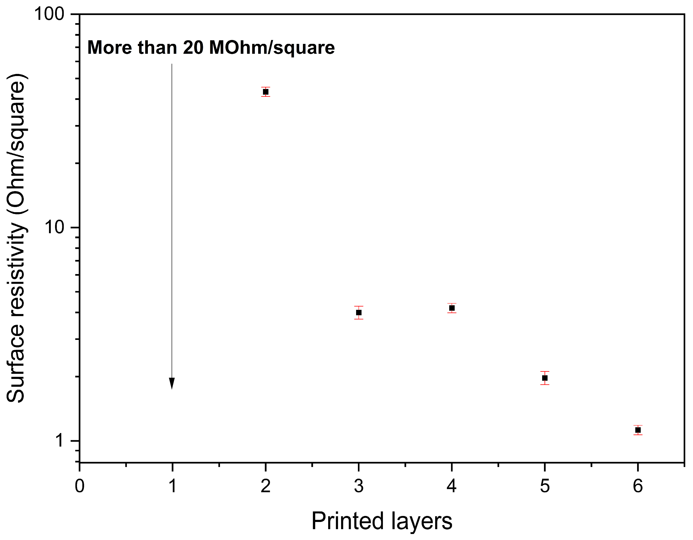
Due to its effectiveness regarding the electrical properties of the printed patterns, we decided to continue using electrospun PCL on baking paper as printing substrate. Patterns with one to six printed layers were printed, transferred and cured, and the electrical conductivity was measured. The results are shown in
Figure 3.
The quantity of layers required to obtain a conductive track after the curing process depends on the local concentration of the metallic nanoparticles and also on the characteristics of the substrate [
21]. For porous substrates, the ink was able to penetrate through the pores among the electrospun fibers, leading to the occurrence of different resistivity levels due to the partial filling of the pores with successive printed layers. Nonporous materials that present conductivity with only one printed layer have been reported and tested, and no diffusion effect was noticed [
23,
24]. In this case, three different levels of resistivity were observed at two, three and five printed layers.
A comparison of sheet resistance and trace width values obtained by various materials and techniques used in printed and conformal electronics is presented in
Table 2. The trace width and resistivities achieved in this work are comparable to those in the recent literature and adequate for most applications for three and more printed layers. Moreover, resistivities were also comparable to those obtained when printing silver inks on nonporous plastic substrates such as PEN.
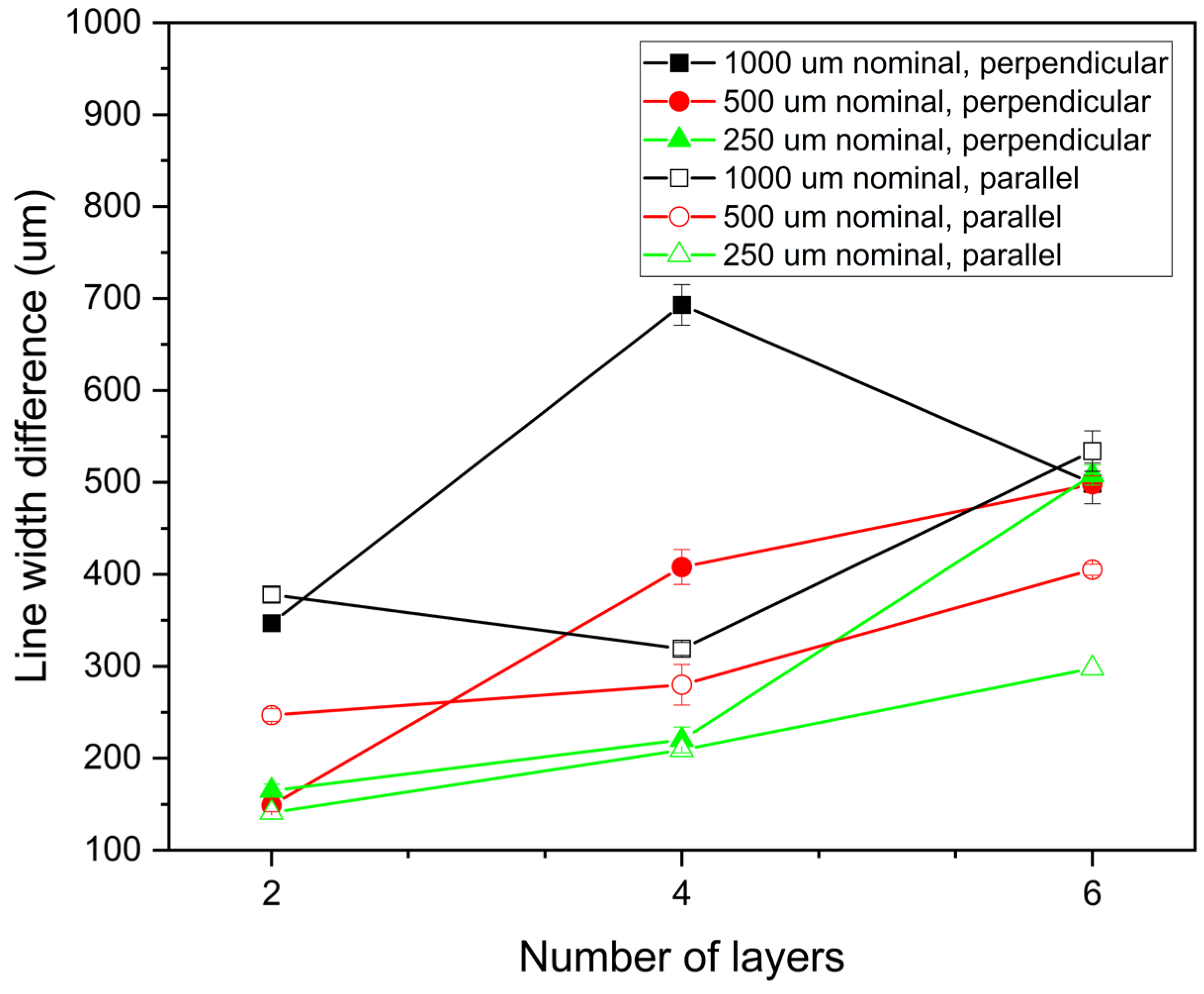
3.2. Morphological Characterization of Transferred and Cured Tracks
Figure 4 shows the line width difference (
WD) using different printing conditions and nominal line widths.
WD was calculated according to the following equation:
where
W_printed is the average line width calculated from 15 samples from each printed line and
W_design is the nominal line width. The
WD was calculated for tracks printed parallel and perpendicular to the fibers’ orientation.
It could be noticed that the printed lines are wider than predicted by design. This is due to the porous nature of the substrate that produces some ink spreading. The difference in line width was easily noticeable, ranging from 150 to 700 microns, and increased with nominal width and the number of printed layers, as expected. The porous characteristics of the electrospun substrate also influenced the line width difference, since it was larger when lines were printed perpendicular to the fibers. However, the line widths were reproducible, showing a maximum standard error of 22 microns. Regarding these results, it is possible to establish coherent design rules for printing conductive tracks onto electrospun PCL using silver nanoparticle inks. However, it is very important to carefully control the electrospinning process to obtain reproducible results with different batches of electrospun substrates.
Transfer and curing processes were carried out at 80 °C and 145 °C, respectively. During the transfer process, we noticed a thermal contraction effect. Dimensional differences after curing process were measure for printed patterns with 500 µm width (by design) and are shown in
Table 3.
Shrinkage was observed for both senses (parallel and perpendicular to fibers’ orientation) but was larger when perpendicular to the fibers, as expected, due to the pore morphology of the electrospun mat. Moreover, the shrinkage after curing was lower, as the number of printed layers increased due to the presence of higher loads of metallic nanoparticles inside the pores of the substrate.
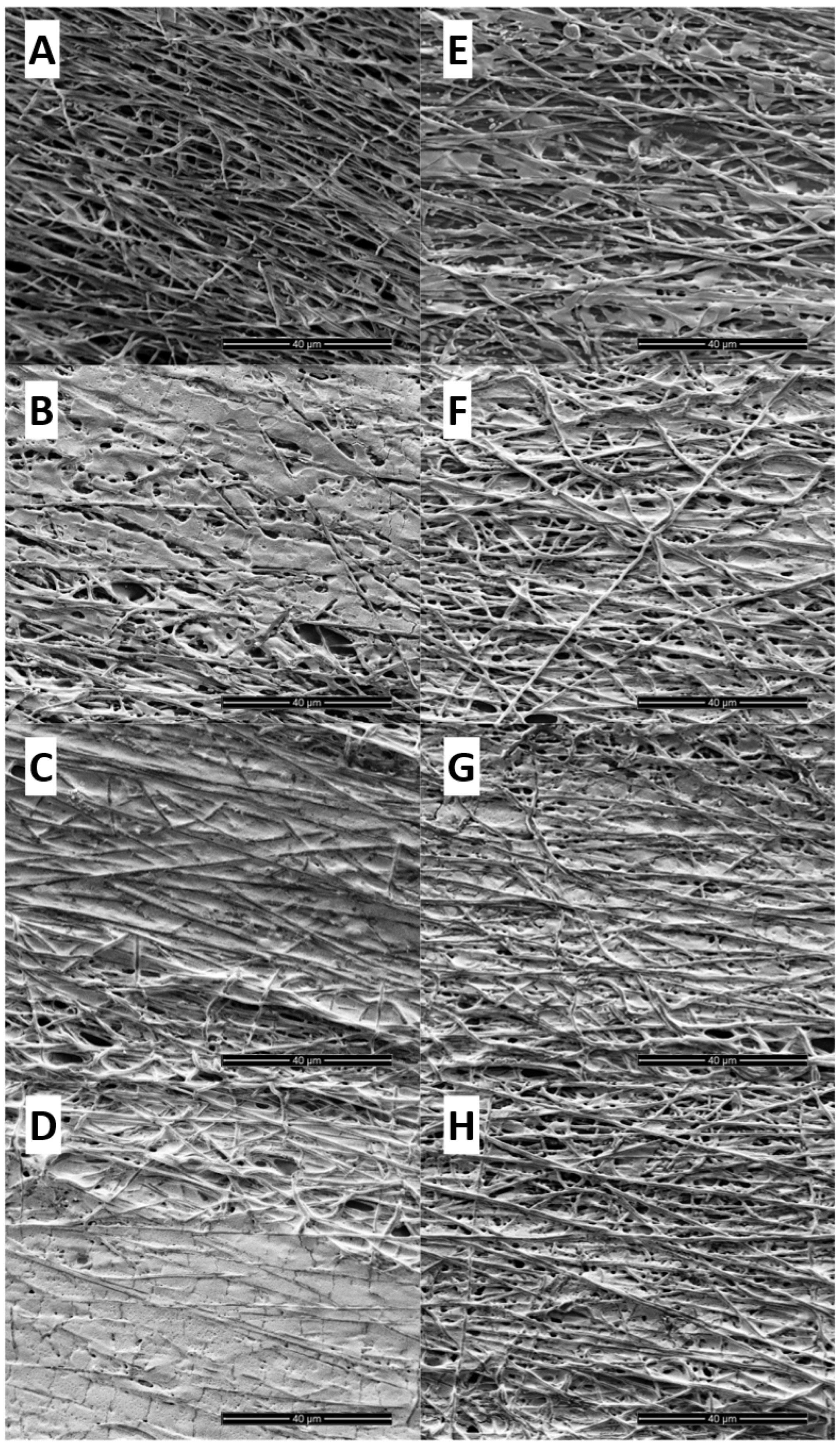
SEM images of printed patterns with one to six printed layers before and after transfer and curing process were taken.
Figure 5 compares the front and back sides of the printed PCL electrospun mat for one, three, five and six printed layers. The occurrence of an ink diffusion process by the concentration of most of ink on the back side could be observed (
Figure 5E). This trend changed for three printed layers, showing both sides almost full of ink. Moreover, the saturation of the pores on the front side occurred at six printed layers (
Figure 5D).
These results confirmed ink diffusion through the pores of PCL electrospun fibers. Silver ink diffusion trough porous substrates was previously reported by other authors regarding printed electronics applications [
22,
23,
24]. The intensity of the diffusion process depends on the porosity and the affinity of the ink to the substrate. This phenomenon also affects the quantity of printed layers needed to obtain an electrically conductive pattern after curing.
Ink buildup allows both sides of the electrospun PCL mats to be conductive and, in turn, interconnect with each other, allowing different printed designs to be electrically connected by simply overlapping them, regardless of which is transferred first and without the need to be transferred at the same time.
Transfer and curing steps produce contraction and melting on the PCL electrospun fibers, as can be observed, especially in
Figure 6A. Upon coming into contact with a piece at 80 °C, fibers melt and merge with neighboring fibers, forming larger-diameter fibers and, in turn, leaving voids on the surface. It is noteworthy that this effect decreased with increasing printed layers (
Figure 6B–D). In addition, it was observed that the fibers within the ink layer did not show large structural changes after transfer at 80 °C. This phenomenon is due to the fact that the pores of the fibers are filled with silver ink, which prevents their agglomeration, maintaining a structure similar to that before the transfer.
In the case of cured fibers, thermal contraction was observed, especially in the mat with one printed layer, revealing inhomogeneities with voids of 17 µm on average. For the fibers with one layer, a rough film with holes was observed, where the fibrillar structure was completely lost. Thermal contraction was markedly lower for the fibers with three, five and six layers, where the fibrillar structure was maintained, although with the appearance of some voids. The SEM images are in accordance to the electrical resistance measurements (
Figure 3) and track width measurements after curing (
Table 3). Ink filling from three and more printed layers prevents the contraction of the printed tracks and provides a continuous path of sintered silver for electrical conduction.
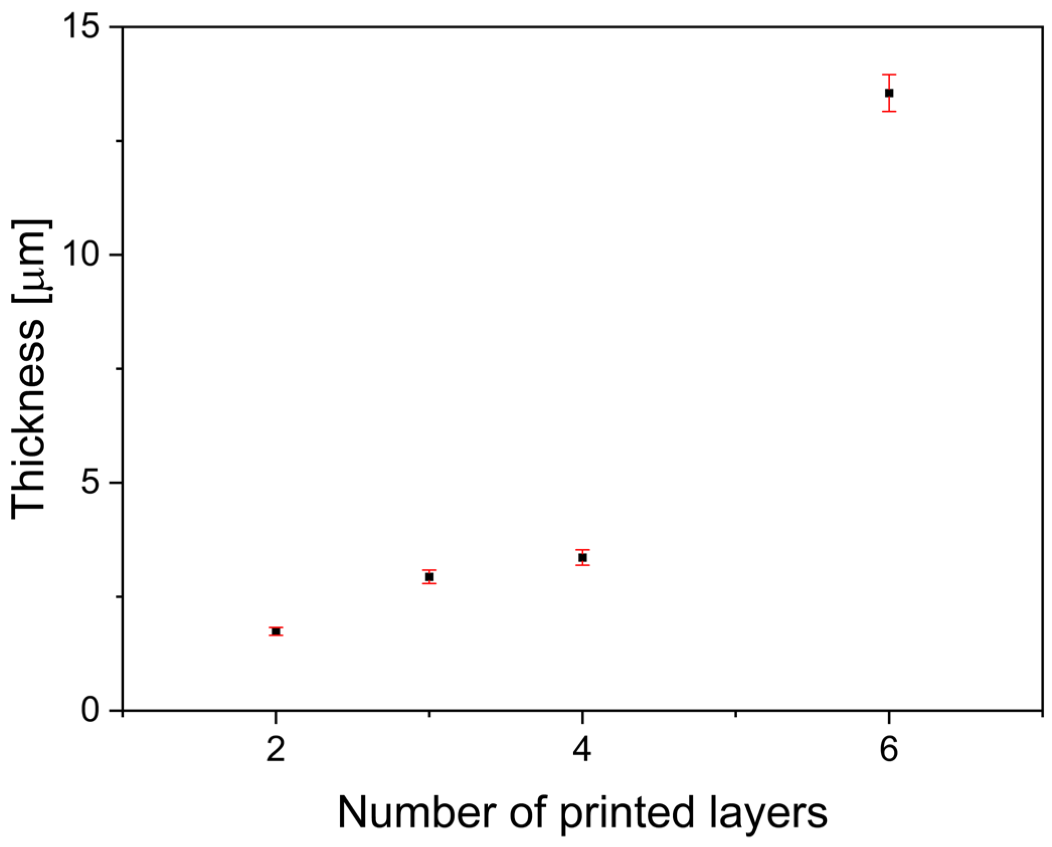
The profilometry of printed tracks with two, three, four and six printed layers transferred and cured onto a PET film is shown in
Figure 7.
The printed tracks showed a larger thickness than the PCL electrospun mat. The two-printed-layer track was 1.74 μm thick, whereas the three- and four-layered tracks were 2.94 and 3.36 μm thick, respectively. A large increase in track thickness was observed for six printed layers (13.55 μm). This behavior could be explained by the diffusion of the ink through the porous matrix until saturation. Once the pores were fully filled with ink, each layer led to a higher thickness after the curing process.
3.3. Adherence of Printed and Transferred Patterns
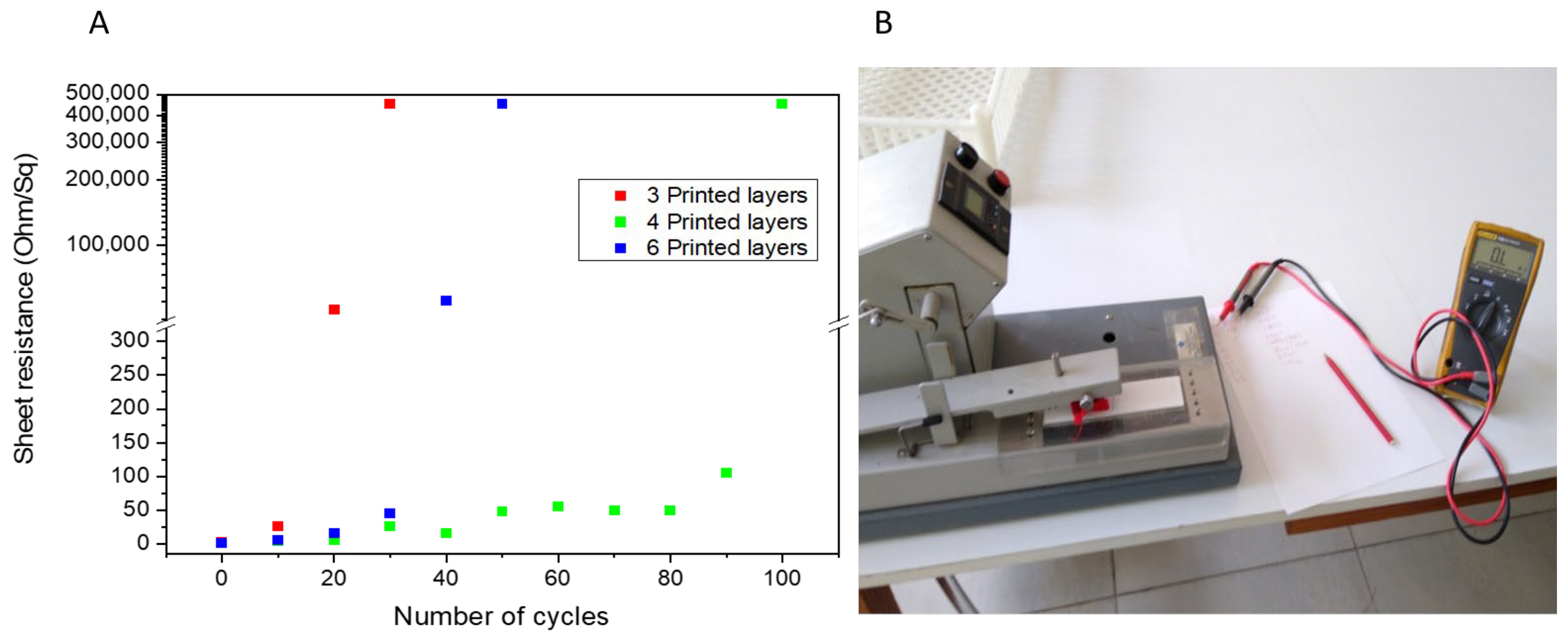
To evaluate adherence and mechanical properties of the printed tracks, a rub resistance test based on standard ISO 105-A01:2010-01 [
20] was performed on printed tracks with three, four and six printed layers. Printed patterns transferred to PLA 3D-printed pieces and cured were assayed using the apparatus shown in
Figure 8B. The rub cycles were performed perpendicular to the track. Electrical resistant measurements were performed after 10 cycles (each cycle includes two rub steps onto the transferred design). The results of electrical resistance after rub cycles are summarized in
Figure 8A.
The samples with three layers underwent changes in their electrical resistance in the first 10 cycles, increasing the resistance by one order of magnitude, while, after 20 cycles, the increase in electrical resistance was three orders of magnitude, losing all functionality after 30 cycles. The samples with four and six layers showed practically no change until after 20 cycles. After 30 cycles, an order-of-magnitude increase in resistance was observed in both samples. Samples with four layers remained close to that value until after 80 cycles and lost functionality after 100, while the samples with six layers began to lose functionality after 40 cycles with an increase in electrical resistance of four orders of magnitude and lost it completely after 50 cycles.
The rub resistance test shows that increasing the number of layers has consequences on mechanical properties and cohesion, as well as electrical conductivity. To understand this behavior regarding rubbing and the failure mechanism, SEM images of all the samples that were subjected to rubbing were taken, and the images before and after failure were compared.
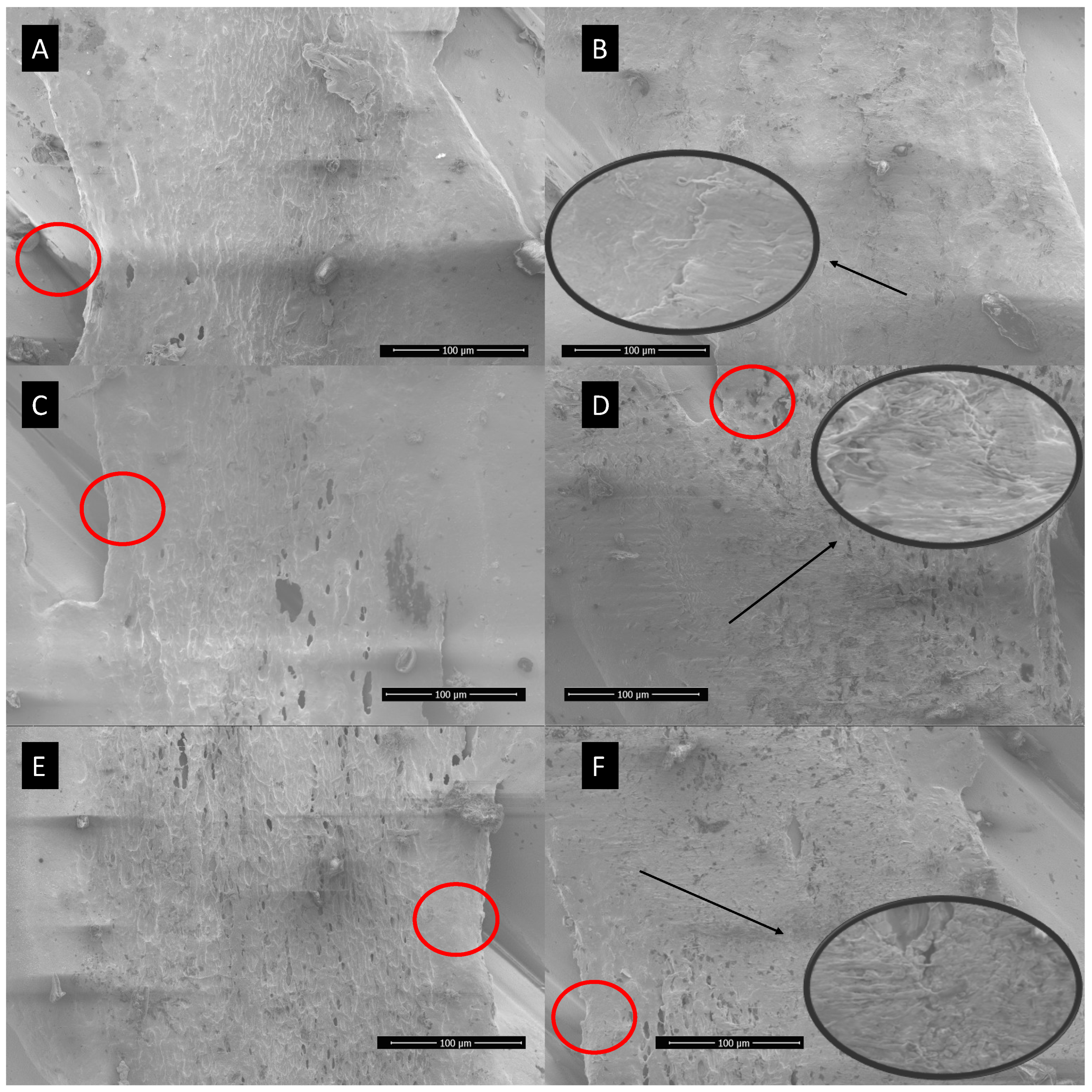
Figure 9A shows images of the zone subjected to rubbing before and after the loss of functionality due to rubbing the lines with three, four and six layers.
SEM images after rubbing (
Figure 9) show that tracks were affected by rubbing. The printed silver layer has been dragged with the passes in every case. It was also observed that there is an influence of the 3D-printed layer on the rub resistance. This is because fused-filament 3D printing is an additive technique that fuses filament lines one beside the other, inevitably leaving grooves and ridges along the surface. It is clearly observed that the fibers attached to a groove sector remained adhered to the 3D-printed surface, while those on a ridge were pulled out from the surface.
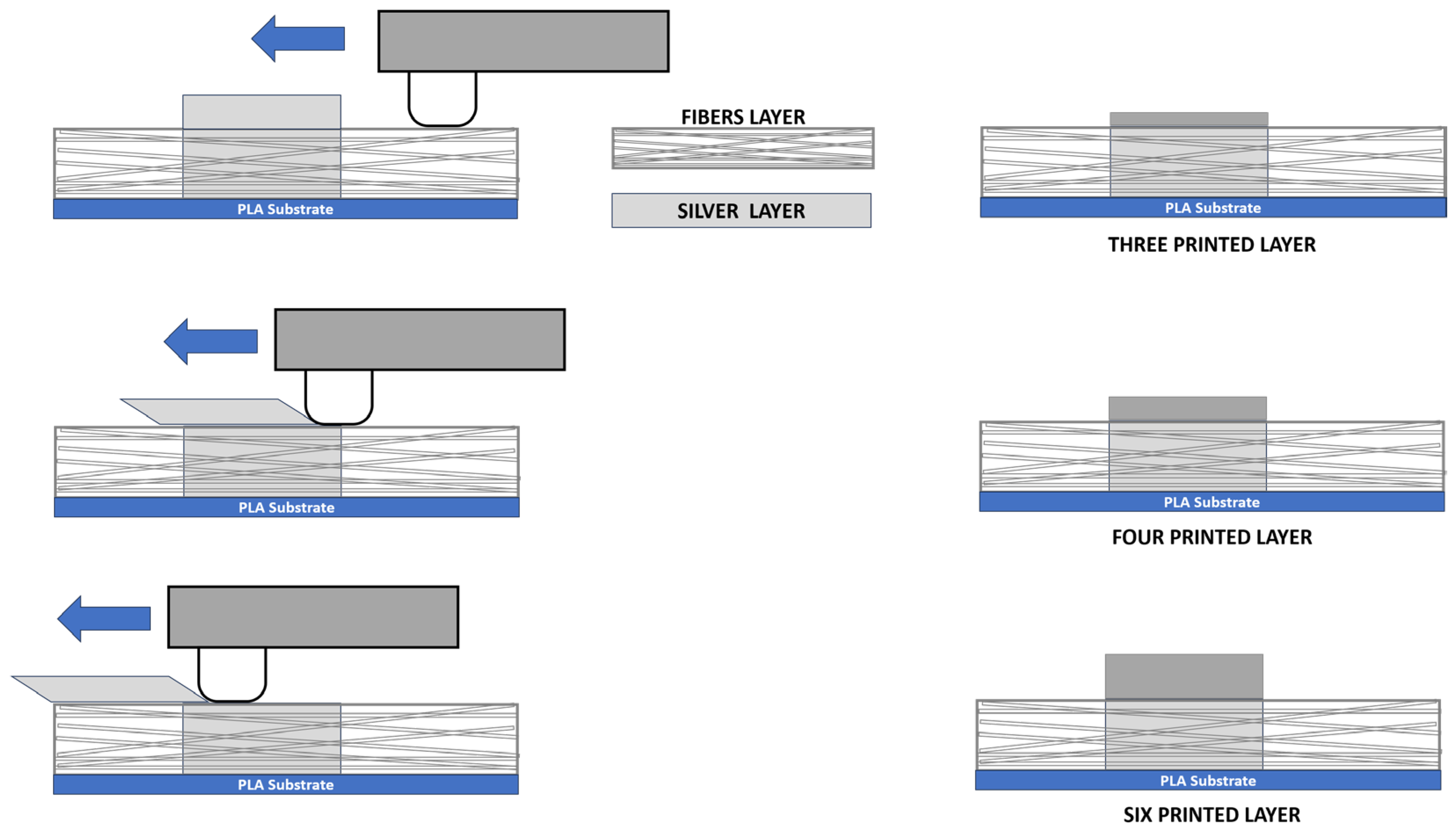
The results can be explained through considering that the ink layers are sintered. By increasing the thickness of the layer, there is a higher concentration of particles and, therefore, better initial conductivity. On the other hand, a thicker layer of sintered ink has greater resistance to rubbing. It is expected that the ink layer will remain cohesive against the shear stress that occurs during rubbing. First, the greater the number of layers, the larger the thickness of the cured pattern. Therefore, the resistance increases more with higher number of layers, due to higher shear stress, as exemplified in
Figure 10. On the other hand, by increasing the number of printed layers, saturation of the pores with ink was observed. The greater the saturation of the pores, the greater the mechanical resistance to shearing of the pattern, because it will have less chance of deformation as the cloth passes.
The first mechanism allows us to explain the differences between the samples with three and four layers and the one with six layers, where a difference of 300% was observed in the thickness of the conductive silver track. On the other hand, the thickness of the deposit with three and four layers presented little variation among themselves. The tracks with six layers, although presenting a more solid structure due to having a greater filling of the pores, has a much greater thickness that generates a larger shear stress during rubbing. Although there were no significant differences in thickness between the tracks with three and four layers, the track printed with four layers will have a higher saturation of silver particles within the fibers, and thus the accumulation of particles not only generates more conductive channels but also gives greater toughness to the mechanical assembly formed by the fibers and the neighboring sintered silver nanoparticles. This feature allowed the system with four layers to achieve greater resistance to rubbing cycles.
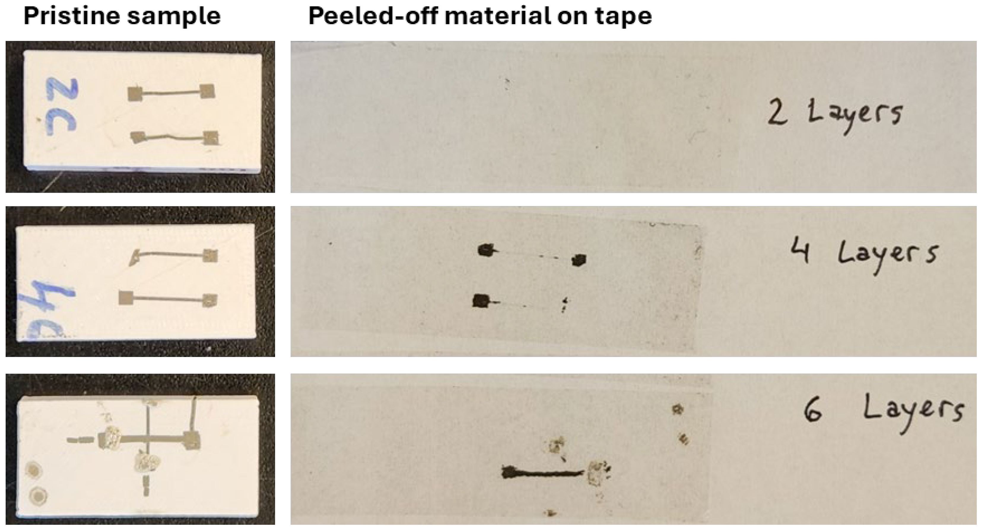
Adherence tests were performed on traces printed with different numbers of layers and transferred to PLA pieces. Scotch tape was used to peel off weakly bound material from the surface. The results are presented in
Figure 11.
It could be noticed that for two layers the tape did not remove a significant amount of material. The traces remained conductive after the test, although they maintained a relatively high resistivity of 40 Ω/square. On the other hand, traces printed with four and six layers were subjected to intensive remotion of printed silver, leading to a loss of conductivity. These results are coherent with the hypothesis of the ink filling and saturating the pores of the PCL mat derived from resistivity measurements, profilometry, SEM images and the rub resistance test. Traces with two printed layers retain most of the ink within the PCL pores, which results in relatively high sheet resistance but strong adherence of the silver to PCL and PLA. On the other hand, traces printed with four and six layers show sheet resistance comparable to that of traces printed on nonporous substrates, because PCL pores are completely saturated with ink and thus a continuous layer of silver can be formed on top of the PCL layer. However, these conductive layers are not as mechanically stable as those printed with two layers.
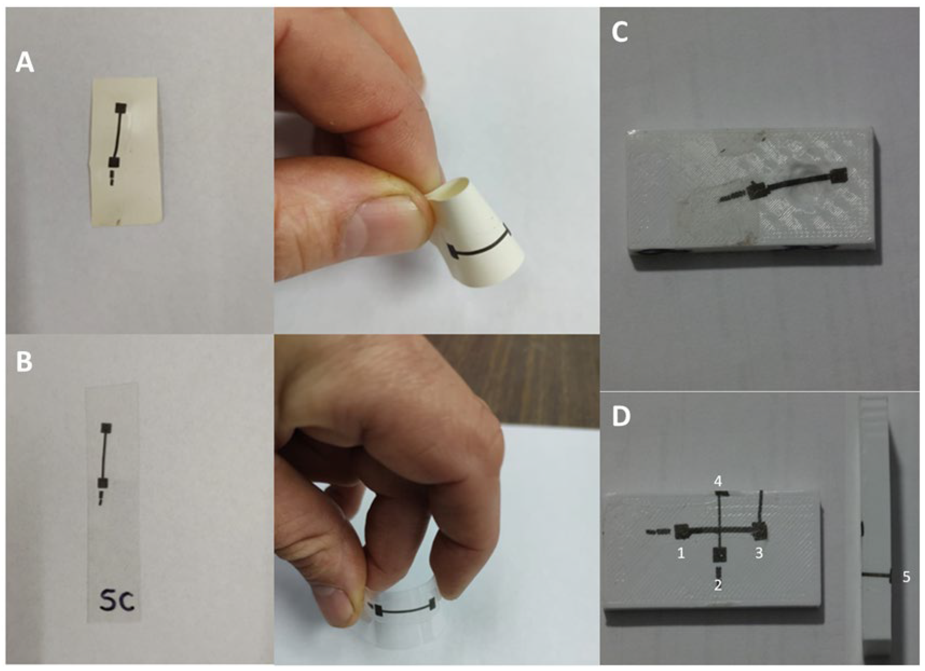
3.4. Tracks Transferred to Non-Planar Surfaces and Flexible Acceptor Substrates
In order to demonstrate the application of the transfer to different topologies and receptor substrates, different printed patterns were printed and transferred to PLA 3D-printed surfaces (planar, with concavities and sharp edges), flexible PET film and elastic TPU film, as shown in
Figure 12.
All the patterns showed electrical conductivity after the curing process, regardless of the topology and composition of the receptor substrate. The electrical conductivity of the tracks transferred to flexible substrates of PET and TPU was measured with mean values of 3 and 4 Ω/Square, respectively, and they maintained their conductivity after bending.
The occurrence of the ink diffusion process led to the presence of ink on both sides of the fiber mat, which allows the connection of two different printed tracks that are transferred separately. In order to prove this assumption, different printed patterns were transferred, partially overlapping one on top of the other, and cured in separate steps, as shown in
Figure 12D. Their electrical surface resistivities are summarized in
Table 4.
Electrical continuity was verified even after connecting patterns in different transfer and curing steps or by transferring a printed track from one side to the opposite of the 3D-printed piece, passing by sharp 90-degree edges. Thus, this system demonstrated to be modular and adaptable to different surface topologies. Modularity is a desirable property in this kind of system due to the possibility of modifying, enlarging or repairing previously transferred and cured circuits.
An interesting feature arises from the adhesion test performed on the modular system (
Figure 11, six layers). The removal of material occurred only in the trace that was placed on top, which indicates that the transfer of a PCL electrospun mat on top of a conductive trace serves as a protective layer that enhances the mechanical stability of the conductive material. These conductive traces were demonstrated to be stable over time. The resistivity of the same conductive printed tracks was measured after two years and did not show any significant differences.


