Article

Optical System of a Prism–Grating Short-Wave Infrared Spectrometer for Single-Pixel Imaging

1
Hangzhou Institute for Advanced Study, University of Chinese Academy of Sciences, Hangzhou 310024, China
2
Shanghai Institute of Technical Physics, Chinese Academy of Sciences, Shanghai 200083, China
3
University of Chinese Academy of Sciences, Beijing 101408, China
*
Authors to whom correspondence should be addressed.
Optics 2026, 7(3), 39; https://doi.org/10.3390/opt7030039
Submission received: 3 April 2026 / Revised: 4 May 2026 / Accepted: 12 May 2026 / Published: 29 May 2026
(This article belongs to the Topic Optical and Laser Scanning: Systems and Applications)

Abstract

To circumvent the prohibitive cost of large-format infrared focal plane arrays and the significant spatial–spectral mismatch caused by spectral smile in conventional long-slit configurations, this work develops a low-cost short-wave infrared (SWIR, 1000–2500 nm) hyperspectral imaging system utilizing digital micromirror device (DMD) scanning paired with a single-element detector. A comprehensive analytical model for a prism–reflection grating (P-RG) compound dispersive element is established, enabling the joint optimization of the prism apex angle and grating period to achieve quantitative compensation of spectral distortion across the entire waveband. Based on this model, the optical system is integrated and optimized, while a centroid localization algorithm is implemented to facilitate online calibration of model parameters and real-time reconstruction of the hyperspectral data cube at the DMD plane. Experimental results demonstrate that both smile and keystone distortions are suppressed below 5 μ m throughout the 1000–2500 nm range, which is superior to the single DMD pixel pitch of 7.6 μ m . The full-field modulation transfer function (MTF) at the Nyquist frequency (32.9 lp/mm) exceeds 0.7, approaching the diffraction limit. Characterization confirms that the system provides 510 spectral channels with an average resolution of 3.57 nm and a spatial resolution of 2.5 μ m . By effectively eliminating spectral overlap and cross-column crosstalk on the DMD encoding surface, this system provides a high-fidelity optical front-end for single-pixel imaging, offering a viable technical pathway for the development of affordable SWIR hyperspectral instrumentation.

1. Introduction

The short-wave infrared (SWIR, 1000–2500 nm) band contains a wealth of material spectral fingerprint information. The overtone and combination absorption peaks of numerous organic molecules (e.g., compounds containing –OH, –NH, and –CH bonds) and inorganic materials present narrow-band structures, with peak positions and profiles demonstrating high material specificity [1,2]. Hyperspectral imaging (HSI) technology constructs a three-dimensional hyperspectral data cube by synchronously acquiring the two-dimensional spatial images and continuous spectral information of a target. This technology holds significant scientific and commercial value in numerous fields such as nondestructive testing, industrial sensing, biomedical diagnostics, geological exploration, and precision agriculture [3,4,5]. If the spectral resolution of the system is insufficient, it will lead to the broadening of characteristic peaks or even the overlapping of adjacent peaks, severely degrading the accuracy of material classification and the reliability of quantitative analysis. In the 1000–2500 nm band, the full width at half maximum (FWHM) of typical organic overtone absorption peaks can be as narrow as the 10 nm scale; therefore, a spectral resolution better than 10 nm is a fundamental requirement for effective spectral identification, which imposes stringent constraints on the design of dispersive elements and system integration.
Current mainstream push-broom hyperspectral systems universally rely on high-performance two-dimensional array detectors such as mercury cadmium telluride (MCT) or indium gallium arsenide (InGaAs). The former requires deep cooling and is prohibitively expensive, while the latter suffers from a limited cutoff wavelength, and extended-wavelength variants face similar exponential cost increases, These issues severely restrict the large-scale application of SWIR hyperspectral instruments in the civilian sector [6,7]. Single-pixel imaging technology has consistently attracted extensive attention in the optical field due to its rapid temporal response, high spectral sensitivity, low dark noise, and low cost [8,9]. Currently, the integration of single-pixel imaging with a spatial light modulator, specifically a digital micromirror device (DMD), provides a novel architecture for low-cost hyperspectral imaging [8,9,10,11].
DMD-based hyperspectral imaging systems can be primarily categorized into two main architectures. The first category is based on the compressive sensing framework, where the DMD is placed after the dispersive element to perform Hadamard transform or random coding on the multidimensional spatial–spectral information for image reconstruction. The modulated light is ultimately received by a focal plane array detector in a single shot, thereby significantly reducing imaging time and achieving compressive SWIR hyperspectral imaging [11,12,13]. The second category relies on the mechanical slit framework found in traditional spectrometers. By leveraging the scanning functionality of the DMD, specific orthogonal coding or wavelength filtering is performed to achieve the flexible extraction of specific spectral channels or regions of interest [14,15,16].
This paper proposes a concept wherein the DMD is positioned at the image plane of the imaging spectrometer, utilizing the programmable micromirror array to replace the traditional two-dimensional array detector, and employing a single-element detector to acquire the DMD-modulated signals. In this architecture, real-time hyperspectral imaging on the single-element detector can be achieved via Hadamard coding. Alternatively, an arbitrary number of spectral bands can be obtained by selectively modulating DMD pixel columns, and the desired spectral resolution can be selected through time-multiplexed framing of DMD pixels. Therefore, it is necessary to prevent mutual interference among spectral information and to maintain imaging accuracy under extremely low-sampling-rate conditions.
Smile and keystone are the two geometric aberrations that most directly undermine spatial–spectral mapping accuracy in hyperspectral instruments. Smile refers to the along-dispersion shift of a given wavelength’s focal position as the field angle changes; keystone refers to the transverse drift of a given spatial position across wavelengths. Together they couple the spatial and spectral dimensions in ways that corrupt both radiometric calibration and spatial registration [17]. In a DMD-based system the consequences are especially concrete: if smile exceeds one pixel pitch, adjacent spectral columns begin to overlap on the DMD plane, causing channel cross-talk and wavelength mis-selection. Assembly tolerances compound the problem—small decenter or tilt errors during integration introduce additional spatial–spectral offsets that wavelength calibration must then disentangle [18].
Currently, commercial DMD spectrometer products (e.g., TI DLP NIRscan Nano) employ short-slit and limited-FOV designs tailored for single-point spectral measurements [19], where the impact of smile remains acceptable. However, hyperspectral imagers require a long slit to achieve wide-FOV spatial sampling, which significantly amplifies the smile and spatial–spectral mismatches induced by the dispersive element, making smile control a core challenge in engineering implementations [20,21].
To address the aforementioned challenges, this paper proposes the use of a compound dispersive (P-RG) structure combining a prism and a reflection grating. The grating provides the primary dispersion, while the prism introduces a complementary spectral smile component to quantitatively compensate for the smile generated by the grating, thereby constraining the integrated spectral smile of the combined system to within a single pixel [18,20,22]. Compared to schemes relying solely on Amici prisms or reflection gratings, the P-RG architecture can simultaneously satisfy the dual requirements of high dispersion efficiency and smile correction over a broadband range (1000–2500 nm) [22,23].
Despite the growing interest in P-RG dispersive elements, a systematic analytical framework tailored specifically to DMD-scanning SWIR systems remains absent from the literature. Without such a model, it is difficult to quantitatively trace the interaction between the grating and prism under non-principal-section incidence, or to predict the resulting three-dimensional dispersion and smile distribution with the accuracy required for pixel-level DMD addressing. Furthermore, smile correction strategies that account for the precision demands of DMD wavelength selection are underdeveloped. Closing these gaps—by building a rigorous P-RG dispersion model and coupling it to a spectral reconstruction pipeline—is essential to making sub-pixel smile control tractable. This paper presents a high-precision SWIR hyperspectral optical system developed along these lines. The focus is squarely on the optical hardware foundation: ensuring spatial–spectral mapping accuracy at the DMD plane to prevent uncorrected geometric distortions from undermining the single-pixel encoding and reconstruction process.

2. Materials and Methods

2.1. Operational Principle and Global Scheme

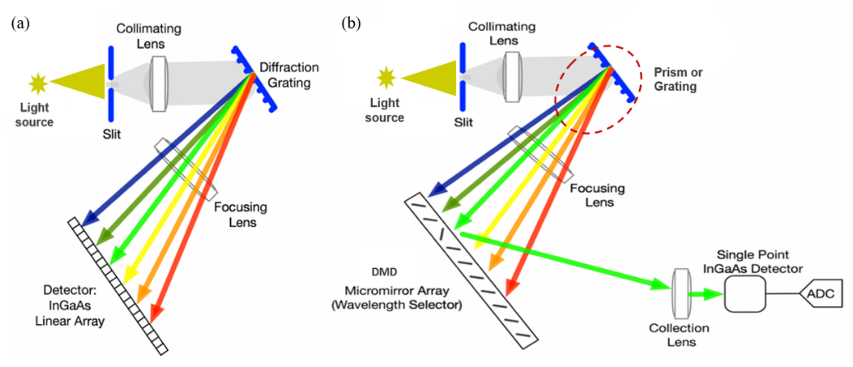
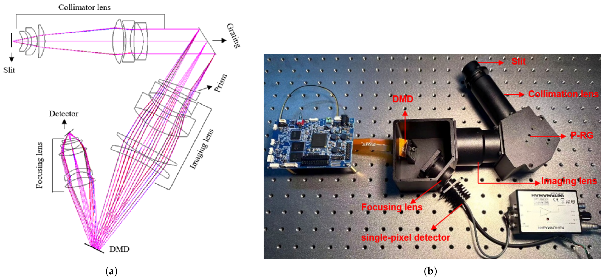
The P-RG short-wave infrared (SWIR) hyperspectral imaging system, based on Digital Micromirror Device (DMD) scanning, comprises a slit, a collimating objective, a prism–reflective grating (P-RG) dispersive element, a focusing objective, a DMD, a condensing lens, and a single-pixel detector. The optical schematic of the system is illustrated in Figure 1. Incident radiation from the target, collected by the fore-optics, enters the system through the slit. It is transformed into parallel beams by the collimating objective and subsequently illuminates the P-RG dispersive module. Light of different wavelengths undergoes dispersion, resulting in differentiated diffraction angles. After being converged by the focusing objective, a one-dimensional dispersed spectral line array is formed on the DMD surface, where spectral columns corresponding to specific wavelengths are mapped to their respective micromirror column positions.
The core engineering constraint of this architecture lies in the requirement that the spectral columns of various wavelengths must remain stable on the DMD plane without experiencing any cross-column broadening. Specifically, both spectral smile and keystone distortions must be strictly confined within the range of a single pixel (7.6 μm) to prevent channel crosstalk and wavelength misselection, which would otherwise compromise the quality and reliability of the hyperspectral data.
In the actual operational workflow, the system leverages the built-in program of the commercial DMD device to perform selective modulation of the spectral columns through row and column addressing. The activated micromirror columns reflect the spectral signals of the corresponding wavelengths into the converging objective lens. Once converged, the total energy response for that specific wavelength channel is recorded by the single-element detector. Unlike a focal plane array, the single-element detector does not capture two-dimensional images directly. Instead, it acquires the signal for each spectral channel sequentially through time-series integration, ultimately reconstructing the three-dimensional hyperspectral data cube.
This sequential readout scheme imposes a stringent engineering constraint on the DMD plane: the stability and registration of spectral columns are paramount. To prevent inter-column leakage, both “smile” (spectral line curvature) and “keystone” (chromatic distortion) must be strictly maintained within the limit of a single pixel pitch ( 7.6 μ m ). Any deviation exceeding this threshold would induce channel crosstalk and wavelength mis-selection, thereby compromising the radiometric integrity and reliability of the reconstructed hyperspectral data.

2.2. Spectral Channel Design via DMD and Detector Specification

2.2.1. Spectral Channel Design via DMD

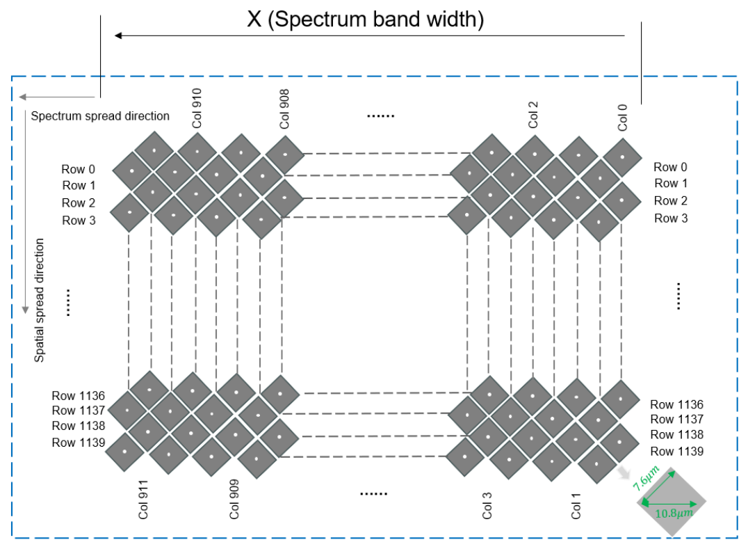
The TI DLP4500 DMD, featuring a 912 × 1140 aluminum micro-reflector array, is positioned at the system’s image plane. Each square micromirror, with a side length of 7.6 μ m , is arranged in a diamond-pixel configuration ( s = 10.8 μ m diagonal). This orientation aligns the spectral dispersion directly with the pixel structure, simplifying the optical layout by eliminating 45° tilt compensation and ensuring normal incidence. The pixel geometry is illustrated in Figure 2. The spectral spread X spanning N columns and the corresponding maximum spectral resolution δ max are governed by:
X = N · s s 2 , δ max = X N
To account for edge blanking and calibration buffers, a 10–20% margin is reserved, reducing the effective array to approximately 821 × 1026 pixels. By adjusting the channel width between 1.5 and 3 columns, the system supports a flexible configuration of 280 to 510 spectral channels. This programmability enables a dynamic trade-off between the signal-to-noise ratio (SNR) and spectral resolution.

2.2.2. Detector Specification

The single-pixel detector chosen for this system is a Hamamatsu G12180-130K (Hamamatsu, Japan), a cooled device with a 900 MHz cutoff frequency and a 3 mm photosensitive aperture. Its performance relative to representative SWIR area-array detectors is summarized in Table 1.
Cost aside, the single-element detector brings two further practical benefits. Its detectivity and quantum efficiency are both higher than those of typical focal plane arrays, which translates directly into better SNR. It also sidesteps the inter-pixel non-uniformity and dark current variation that make flat-field calibration of array detectors a persistent headache.

2.3. Prism–Reflective Grating Combined Dispersive Modeling

2.3.1. Modeling Methodology and Coordinate System Establishment

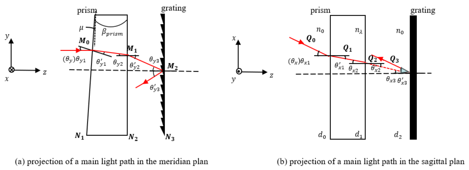
To quantitatively analyze the spectral line curvature (smile) characteristics of the P-RG combined dispersive structure, this study treats the DMD as the emitting surface, while the collimating and imaging lens groups are considered ideal optical systems. Under these equivalent conditions, the initial spatial wave vector Q 0 of the chief ray originating from any DMD micromirror unit—defined in the equivalent space preceding the P-RG module—is identical to the actual incident wave vector at the front surface of the prism. A Cartesian coordinate system is established along the y-x-z directions, with the optical axis acting as the z-axis. The schematic of the P-RG module is illustrated in Figure 3.
In the figure, n x denotes the refractive index of each medium, d x represents the thickness of each medium along the optical axis, N x is the unit normal vector of each refractive interface (oriented from the incident medium toward the emergent medium), M x indicates the intersection point of the chief ray with each refractive surface, and Q x denotes the unit wave vector of the chief ray propagating within each medium. The initial wave vector Q 0 of an arbitrary chief ray lies within the Z O X plane, whereas the subsequent wave vectors Q 1 , Q 2 , Q 3 , and Q 4 are all treated as spatial wave vectors. The angle θ x is determined by the prism apex angle β prism .

2.3.2. Spatial Dispersion Equations of the Prism

The initial wave vector Q 0 and the normal vector N 1 of the front prism surface are given respectively by:
Q 0 ( θ x ) = ( sin θ x , 0 , cos θ x )
N 1 ( θ y ) = ( 0 , sin θ y , cos θ y )
where θ x and θ y are the projection angles of the chief ray in the X O Z and Y O Z planes, respectively. The incident angle θ 1 at Interface 1 is determined by the dot product:
θ 1 ( θ x , θ y ) = arccos ( Q 0 · N 1 )
According to Snell’s law, the angle of refraction θ 1 within the prism is given by:
θ 1 ( θ x , θ y , n λ ) = arcsin n 0 n λ sin | θ 1 |
Given that the incident ray propagates in a non-principal section direction, an equivalent refractive index N λ must be introduced to describe the spatial dispersion characteristics of the prism. The spatial dispersion equations for the prism are given by:
n 0 sin θ y 1 = N λ sin θ y 1
N λ = n λ 2 + ( n λ 2 n 0 2 ) · cos 2 ( μ θ y 1 ) · tan 2 θ x 1 = n λ cos ( μ θ y 1 ) tan θ x 1 cos ( μ θ y 1 ) tan θ x 1
where μ is the angle between the incident ray M 0 and the optical axis of the prism’s front surface. After refraction by the prism, the emergent projection angles in the meridional and sagittal planes satisfy the following equations, respectively:
tan θ y 3 = tan [ arcsin ( n λ sin ( μ θ y 1 ) ) ]
tan θ x 3 = tan arcsin n λ sin θ x 1 n λ

2.3.3. Dispersion Equations for Non-Principal Section Incidence on the Reflective Grating

Rays from the prism are incident on the planar reflective grating at an arbitrary spatial angle. Let the zenith and azimuth angles of the incident light be θ and φ , respectively, and those of the diffracted light be θ and φ . The three-dimensional (3D) grating vector equations are expressed as:
n m sin θ cos φ = n i sin θ cos φ + m λ d
n m sin θ sin φ = n i sin θ sin φ
where m is the diffraction order, λ is the wavelength, and d is the grating constant. In this system configuration, n i = n m = n 0 = 1 . The incident angle θ 3 is determined by the dot product of the chief ray wave vector Q 2 and the grating normal vector N 3 :
cos θ 3 = Q 2 · N 3 = cos φ cos θ
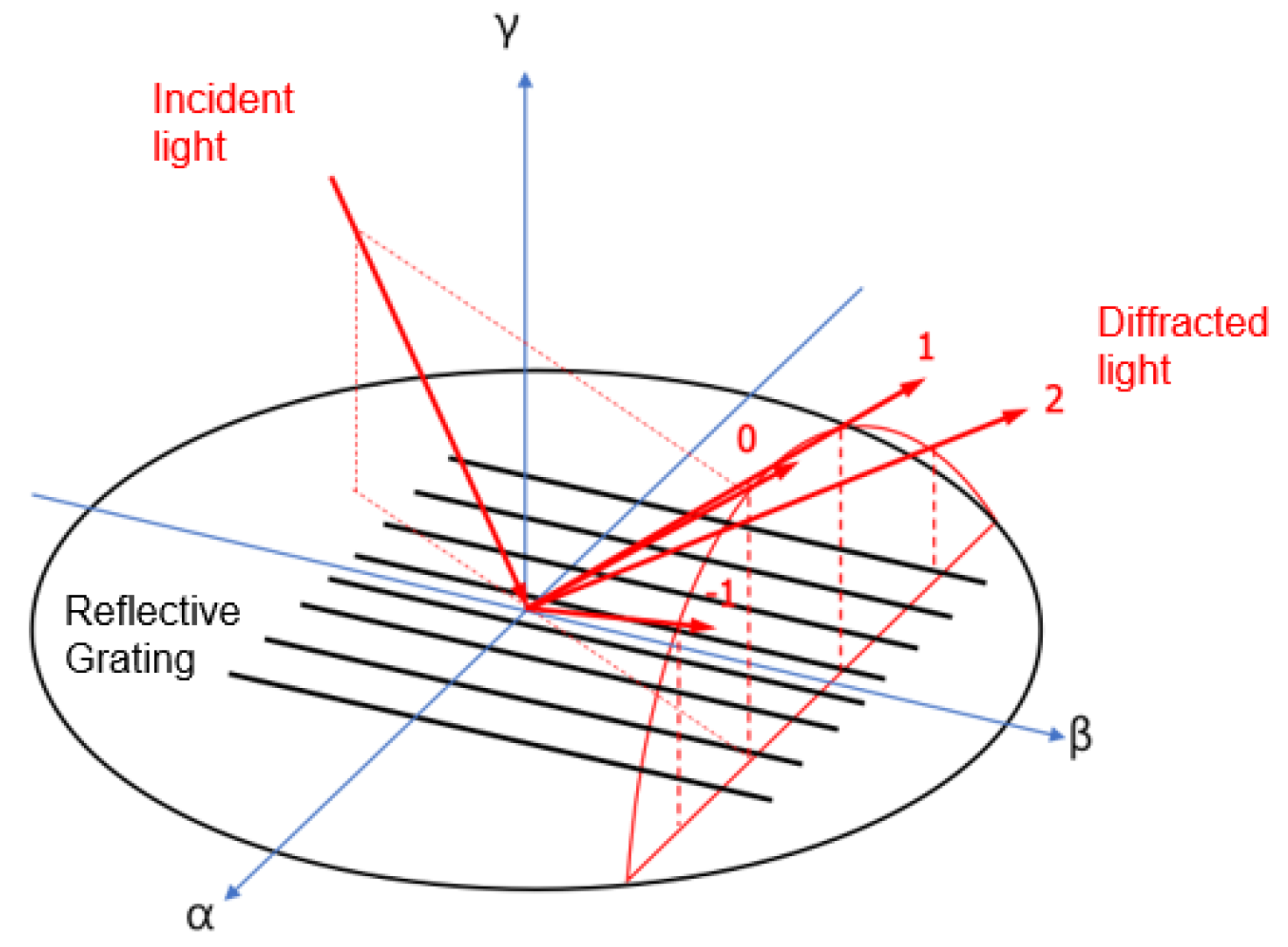
Figure 4 illustrates the 3D diffraction optical path of the chief ray originating from an arbitrary field of view at the grating. Following the right-hand rule, rotation about the z-axis is defined as positive in the counterclockwise direction and negative in the clockwise direction.
The direction angles ( θ x 3 , θ y 3 ) of the diffracted ray are solved using the following system of equations:
sin θ = sin 2 θ sin 2 φ + sin θ cos φ + m λ d 2 = tan 2 θ x 3 + tan 2 θ y 3 1 + tan 2 θ x 3 + tan 2 θ y 3
tan φ = sin θ sin φ sin θ cos φ + m λ d = tan θ x 3 tan θ y 3
φ = arctan tan θ x 3 tan θ y 3
Assuming an inclination angle ε between the reflective grating and the original optical axis, and a rotation angle η of the DMD plane relative to the rear lens group, the image point coordinates ( x , y ) on the DMD plane are given by:
x = f x tan ( ε + θ x 3 )
y = f y tan ( ε + θ y 3 ) cos ( ε + η )
where f x and f y are the equivalent focal lengths of the imaging objective in the two respective orthogonal directions. At this stage, the complete analytical model for the P-RG combined dispersion is established, enabling the precise calculation of the position coordinates for the spectral columns of each wavelength on the DMD plane.

2.3.4. Dispersion Equations for Principal Section Incidence on the Reflective Grating

The magnitude of spectral line curvature (smile), denoted as Δ y , is defined as the image point displacement along the spectral dispersion direction on the DMD plane for the same wavelength across different field-of-view positions:
Δ y = f · Δ θ
where f represents the focal length of the imaging objective, and Δ θ denotes the angular difference in the spectral direction after P-RG dispersion for chief rays originating from different fields of view.
When the prism and grating materials, as well as the diffraction order, are determined, Δ θ is exclusively a function of the field-of-view (FOV) angle θ y , the grating constant d, and the wavelength λ .
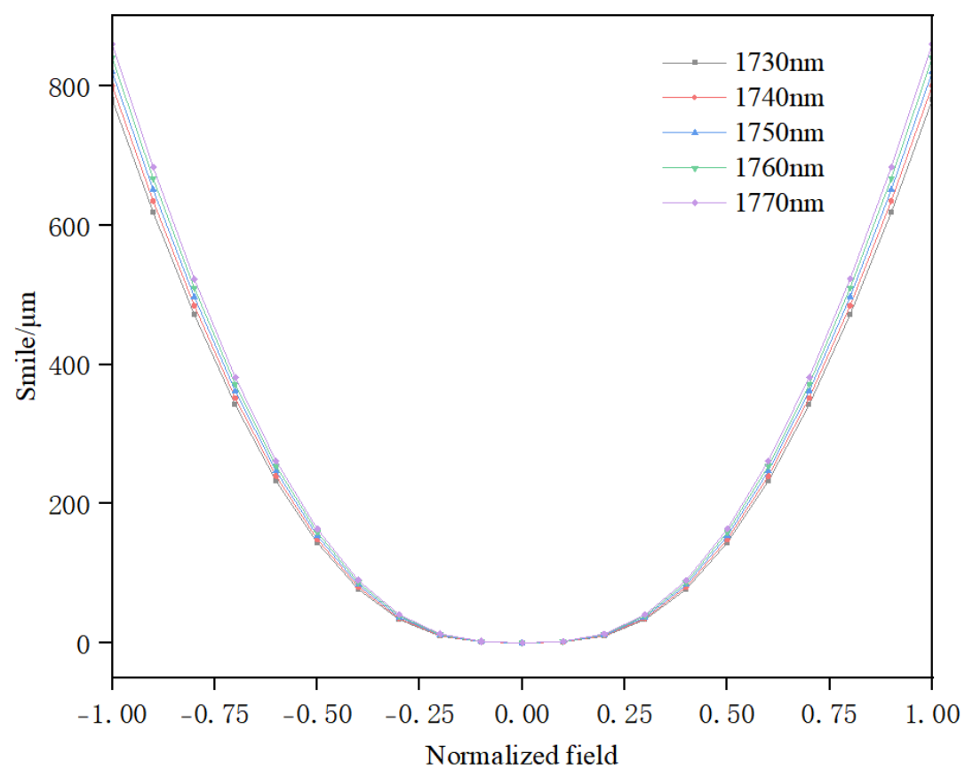
When the reflective grating is utilized independently, non-principal section diffraction causes rays of the same wavelength from different FOV positions to exhibit a pronounced smile shift on the DMD plane. Upon introducing the prism, its inherent spectral line curvature is directed oppositely to the smile shift induced by the grating, thereby enabling quantitative compensation. As previously shown in Figure 5, the spectral line curvature distribution around the 1750 nm wavelength—when the prism apex angle is set to 0° (i.e., pure grating dispersion)—clearly demonstrates the significant smile shift inherent to the standalone grating structure.
The field of view is related to the slit width x. The relationship between the slit width x, the dispersion model, and the focal length of the imaging objective lens can be expressed as:
x = Δ λ · d θ d λ · f = N δ
where Δ λ represents the spectral resolution, f is the focal length of the imaging objective lens, N denotes the number of DMD micromirror pixels occupied by each spectral band, and δ is the micromirror size. Based on Equation (19), we further obtain:
S ( x ) = Δ λ · d θ d λ · f N δ
Here, S ( x ) represents the error between the theoretically calculated slit image width and the designed target experimental width. The magnitude of this error directly reflects the accuracy of the theoretical model.
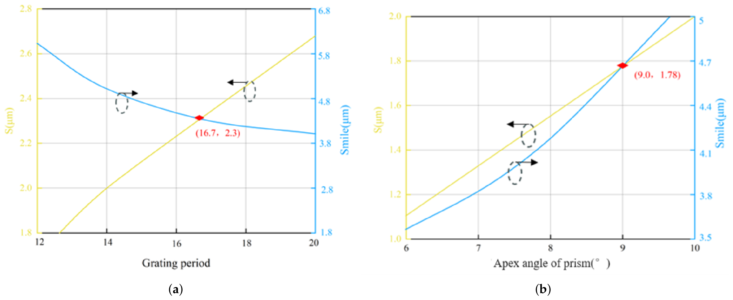
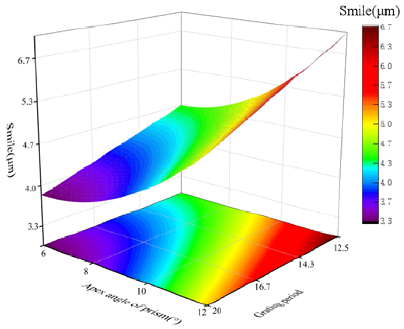
To decouple the influence of the two free parameters—grating period d and prism apex angle β —the latter is initially held at β = 10 ° while d is varied. As illustrated in Figure 6a, S ( x ) and S m i l e ( λ ) (the full-field smile generated by the grating) exhibit an inverse relationship with respect to d. Their curves intersect at d = 16.7 μ m , where both quantities converge to approximately 2.3 μ m , defining the optimal value for the grating constant.
With d fixed at 16.7 μ m , the same optimization procedure is repeated for β . Figure 6b shows that the two curves intersect at β = 9.0 ° . At this intersection, the prism-induced curvature and the grating-generated smile are equal in magnitude and opposite in sign. This condition represents the optimal compensation point, where the two effects mutually cancel to yield the minimum achievable residual modeling error.
Through parameter optimization, the optimal parameter combination for the Prism–Grating (P-RG) composite dispersion module is ultimately determined to be a prism apex angle of β = 9.1 ° (using SiO 2 material), a grating groove density of 60 lines / mm , and a diffraction order of m = 1 . The modeling error distribution of the P-RG module is illustrated in Figure 7. After parameter matching, the residual error of the dispersion modeling exhibits significant convergence.

2.4. Optical System Integration Design

Based on the optimal component parameters determined by the aforementioned P-RG dispersion model, integrated optimization was performed in conjunction with a symmetrical collimating–imaging optical system. Following the integrated optimization design, the primary technical specifications of the system are summarized in Table 2.
The imaging system adopts an image-space telecentric architecture, ensuring that chief rays from all slit positions emerge from the collimator parallel to the optical axis. This configuration allows every point along the long slit to illuminate the P-RG element at a uniform spatial angle, which is a prerequisite for spatially uniform dispersion. Throughout the optimization process, the spectral smile and keystone were treated as hard constraints and strictly restricted to less than one DMD pixel pitch ( 7.6 μ m ), while simultaneously accounting for practical optomechanical alignment tolerances. However, geometric tuning of the prism and grating parameters alone is insufficient to drive the residual smile down to the required level (as shown in Figure 7). To bridge this gap, an additional lens group is integrated into the collimating path. By introducing controlled asymmetric aberrations, this group compensates for the residual smile left by the P-RG geometry, finalizing a high-performance broadband optical layout (Figure 8a).
Lens material selection was driven by the necessity to balance transmittance and dispersion across the full 1000– 2500 nm spectral band. Following iterative substitution and systematic re-optimization, the final material sequence from the slit to the DMD was established, as summarized in Table 3. The resulting Modulation Transfer Function (MTF) shows a noticeable improvement across the entire operational band, with the most significant performance gains achieved at the long-wave infrared end. In this region, chromatic aberrations beyond 2000 nm , which had previously been the most challenging to mitigate, were successfully suppressed to within the design requirements.

2.5. Image Quality Evaluation of the Optical System

2.5.1. Analysis of the Modulation Transfer Function and Spot Diagrams

According to the Nyquist sampling theorem, given a pixel pitch δ as the sampling period, the system’s Nyquist frequency f N is expressed as:
f N = 1 2 δ
In this system, the edge length of the DMD micromirror is 7.6 μ m , which corresponds to a Nyquist frequency of:
f N = 1 2 × 7.6 μ m 65.8 lp / mm
Taking into account the effective sampling interval under the diamond pixel array arrangement, the practical Nyquist frequency of the actual system is designated as 32.9 lp / mm .
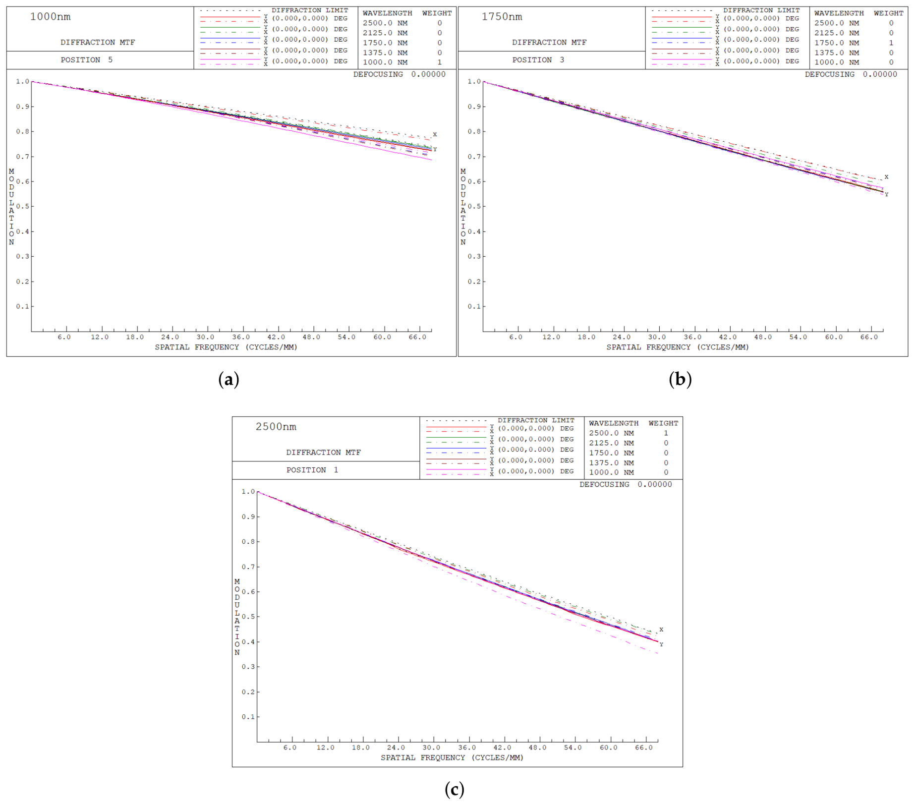
Figure 9 illustrates the MTF curves at the DMD plane for the chief rays across the full field of view (FOV) at three typical wavelengths: 1000 nm , 1750 nm , and 2500 nm . As observed from the figures, at the Nyquist frequency of 32.9 lp / mm , the MTF across the full FOV exceeds 0.7. Across the entire operational waveband, the system’s MTF curves approach the diffraction limit, indicating excellent aberration control. This plays a vital role in ensuring the practical feasibility of the mechanical structure design and alignment of the system.
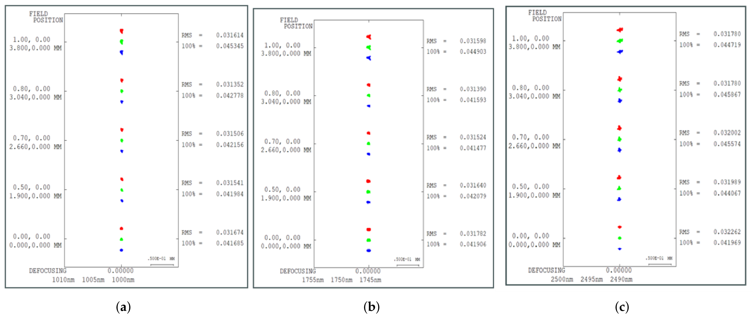
Spot diagrams provide a supplementary characterization of the system’s aberration distribution from a geometrical optics perspective. Figure 10 illustrates the spot diagrams at the DMD plane across various operational wavelengths, given a spectral resolution interval of 5 nm . The imaging spots corresponding to different wavelengths are distinctly resolved, indicating that the intrinsic spectral resolution of the optical system is finer than 5 nm . Furthermore, the focal spots formed by three adjacent wavelengths on the DMD plane are strictly confined within the dimensions of a single micromirror pixel, exhibiting no mutual energy overlap. This confirms that the system can effectively differentiate adjacent spectral channels during the wavelength selection process, thereby satisfying the rigorous engineering constraints required for precise wavelength modulation via the DMD.

2.5.2. Evaluation of Spectral Smile and Keystone

For this system, the design specifications mandate that both smile and keystone must be constrained to sub-pixel levels:
| Δ smile | < δ pixel = 7.6 μ m , | Δ keystone | < δ pixel = 7.6 μ m
To intuitively demonstrate the necessity of the Prism–Reflective Grating (P-RG) compensation, the prism apex angle in the dispersion model was initially set to 0° (meaning the dispersion was provided solely by the grating). Real ray tracing was then performed to obtain the spectral smile distribution near the 1750 nm wavelength, as previously illustrated in Figure 5. It is clearly evident that without the prism’s compensation, the smile offset between the central and edge FOVs significantly exceeds the single-pixel threshold, which would inevitably trigger severe channel cross-talk.
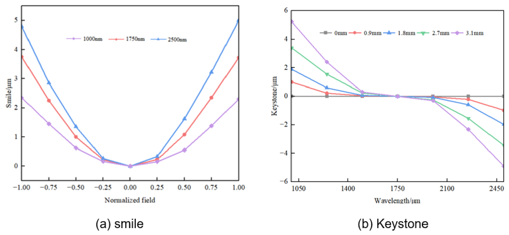
Upon introducing the prism compensation ( β = 9.1 ° , SiO 2 ), the variations in image plane positions across different FOVs and wavelengths were recalculated via real ray tracing, yielding the final smile and keystone distributions, as depicted in Figure 11. Under the three typical wavelength conditions ( 1000 nm , 1750 nm , and 2500 nm ), the maximum spectral smile of the system is reduced to approximately 4.99 μ m , which is well below a single DMD pixel dimension ( 7.6 μ m ). Similarly, the maximum chromatic keystone is restrained to approximately 5.2 μ m , also satisfying the sub-pixel requirement. These results demonstrate that through the judicious parameter matching of the P-RG composite dispersion structure, the spectral-geometric distortions of the system are effectively suppressed, allowing the system to maintain highly stable spatial–spectral consistency over a relatively large FOV and broad waveband.

2.5.3. Tolerance Analysis

The actual performance of an optical system is governed not only by its nominal design but is also significantly influenced by manufacturing errors and alignment deviations. The primary objective of tolerance analysis is to establish allowable manufacturing and assembly tolerances for each optical component, ensuring that the system consistently meets the required performance specifications under practical fabrication and integration conditions.
The allocation of tolerances is governed by the principles of sensitivity analysis. Stricter tolerances are assigned to parameters that exert a substantial impact on the Modulation Transfer Function (MTF), whereas tolerances for MTF-insensitive parameters are appropriately relaxed. This approach strikes an optimal balance between manufacturing feasibility and production costs. The specific tolerance allocation results for the proposed system are detailed in Table 4.
The Monte Carlo analysis results are summarized in Table 5, which presents the MTF values at the Nyquist frequency for five typical wavelengths ( 1000 nm , 1350 nm , 1700 nm , 2050 nm , and 2500 nm ) under varying confidence probabilities.
The observed decline in the Modulation Transfer Function (MTF) at 2500 nm is consistent with physical expectations: material transmittance tends to decrease at longer wavelengths, and the diffraction limit itself scales linearly with wavelength, both of which inherently suppress the MTF response. Taken as a whole, the established tolerance budget ensures that the system remains manufacturable and alignable within conventional precision fabrication capabilities.

3. Experimental Verification and Results Analysis

3.1. Experimental System Construction

Based on the optical system design scheme presented in Section 2, a prototype of the P-RG type short-wave infrared (SWIR) hyperspectral imager was constructed, with its experimental optical layout illustrated in Figure 8b.
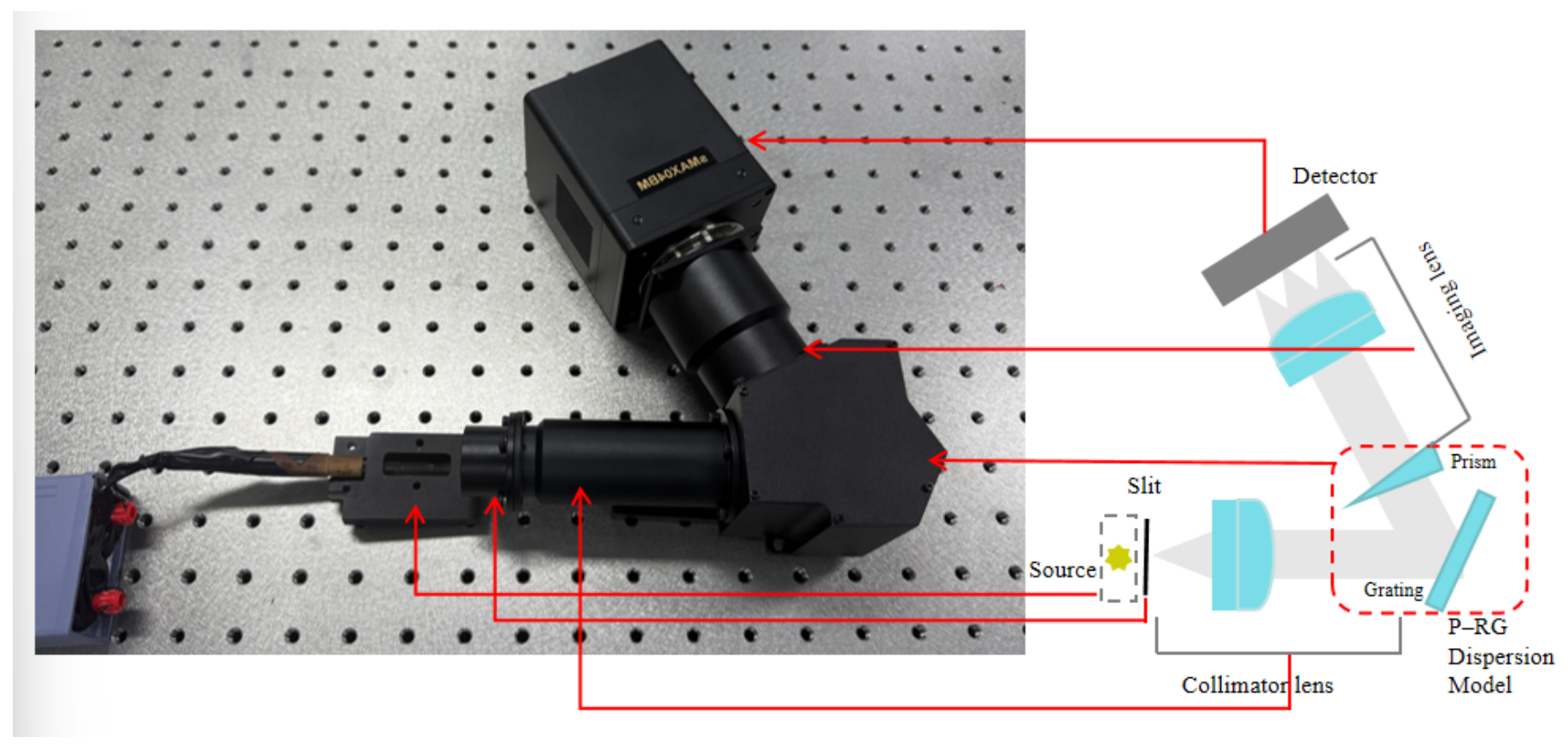
To evaluate the intrinsic imaging quality of the P-RG front-end optics in isolation—thereby decoupling the results from variables introduced by subsequent DMD encoding and single-pixel reconstruction—a dedicated verification path was implemented (Figure 12). In this configuration, an area-array CCD camera is substituted for the DMD at the system focal plane to record the dispersed spectral stripes in real time. This arrangement provides direct access to core performance metrics, such as spectral smile, keystone, and spatial resolution, without the confounding effects of downstream signal processing. These measurements establish the optical hardware baseline against which subsequent single-pixel imaging performance can be benchmarked.

3.2. Wavelength Calibration Experiment

3.2.1. Mercury Lamp Test

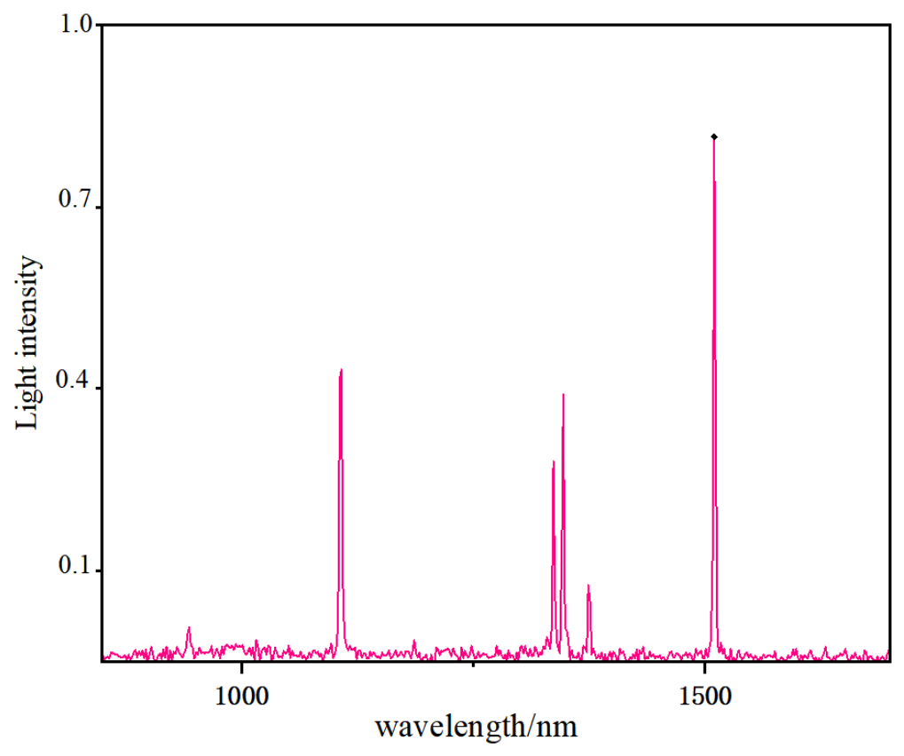
Assembly tolerances and residual aberrations inevitably cause the dispersed spectral columns to shift from their designed positions on the DMD plane, thereby corrupting the wavelength-to-spatial mapping. To re-establish this relationship, an Ocean Optics Hg/Ar lamp was employed as a reference source. By measuring the positions of several characteristic emission lines with precisely known wavelengths in the 1000– 1530 nm range, these data were fed back into the P-RG dispersion model to inversely solve for alignment offsets and correct the mapping. The resulting spectral image of the mercury lamp is illustrated in Figure 13.
Specifically, a centroid algorithm is employed to extract the precise spatial coordinates of these spectral lines on the detection plane. By comparing these measured coordinates with the theoretical positions predicted by the P-RG model, the global displacement parameters are determined. Subsequently, a broadband extrapolation calibration is performed across the entire 1000–2500 nm spectral range. This procedure achieves an accurate broadband wavelength-to-spatial mapping calibration and effectively compensates for the spatial–spectral offsets introduced during the actual alignment process.

3.2.2. Monochromator Performance Test

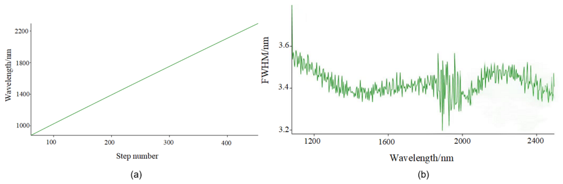
Full-band calibration was performed by stepping an Omni- λ 750i monochromator (Zolix; spectral resolution: 0.028 nm ; operating range: 1000– 2500 nm ) through 510 discrete channels spanning the operational band. The system response was recorded at each step to accurately extract the instrument line shape (ILS). The correspondence between the monochromator channels and the wavelengths is illustrated in Figure 14a.
Experimental results indicate that the system maintains a stable narrow-band response across the entire 1000– 2500 nm range, achieving an average spectral resolution of 3.57 nm with high linearity. The relatively lower resolution observed at the short-wavelength end is primarily attributed to residual geometric aberrations induced by material dispersion. Conversely, the slight degradation in resolution beyond 2000 nm is mainly due to decreased system responsivity. Nevertheless, the overall trend remains smooth without anomalous spectral broadening, demonstrating that the P-RG dispersive architecture sustains high diffraction efficiency and robust spectral imaging performance across a broad band.

3.2.3. Single-Pixel Detector Resolution Test

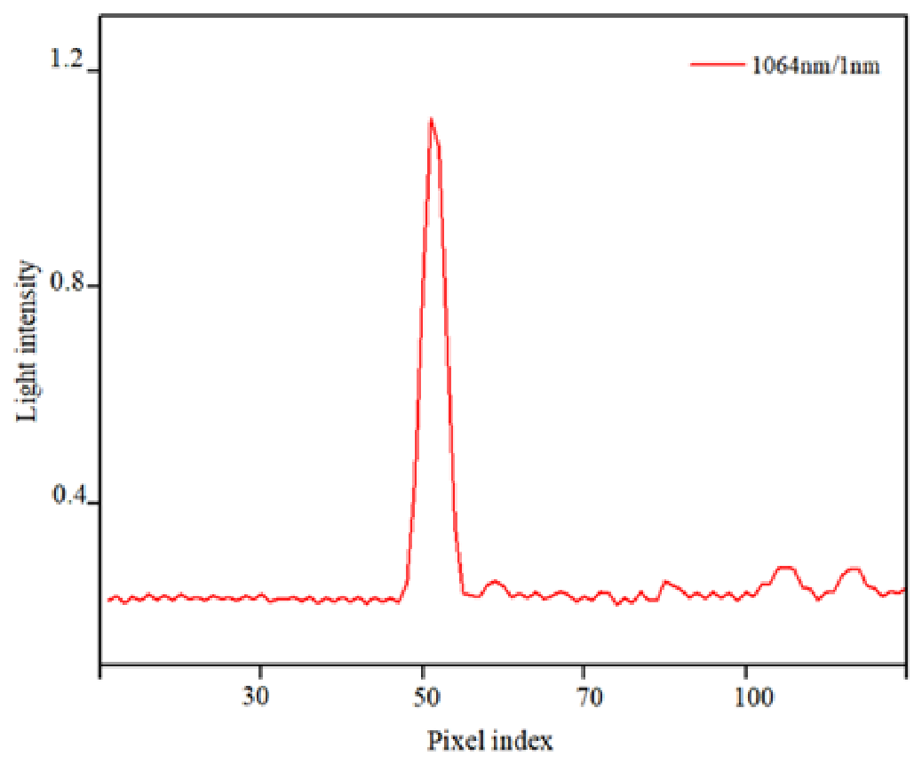
To further validate the spectral resolving power of the system at the single-pixel detector terminal, an experiment was conducted using the P-RG short-wave infrared (SWIR) hyperspectral imager prototype. An Argon (Ar) laser with a precisely known wavelength was employed as the standard point light source. During the measurement, the first 30 columns of the DMD micromirror array were selected and divided into groups of four columns. These groups were sequentially activated starting from the first column, and the corresponding response signals from the single-pixel detector were recorded for each gating state. As illustrated in Figure 15, the measured full width at half maximum (FWHM) of the Ar laser spectral line is 4.08 nm. This experimental result is in excellent agreement with the theoretical value predicted by the optical design, demonstrating that the prototype can stably resolve adjacent spectral channels, thereby satisfying the fundamental requirements for subsequent SWIR hyperspectral image reconstruction.

3.3. Hyperspectral Imaging Experiments

3.3.1. Laboratory Imaging Experiments

To validate the spectral scanning and imaging capabilities of the proposed DMD-based prism–grating short-wave infrared (SWIR) hyperspectral optical system, comprehensive imaging experiments were conducted on the front-end optics preceding the DMD. These evaluations were designed to directly assess the spatial–spectral consistency at the DMD image plane and the imaging stability under field push-broom conditions. Such validations are crucial for subsequent DMD-based encoding algorithms and the reconstruction of hyperspectral data at the single-element detector—a configuration essential for realizing low-cost, high-signal-to-noise-ratio (SNR) single-pixel SWIR imaging.
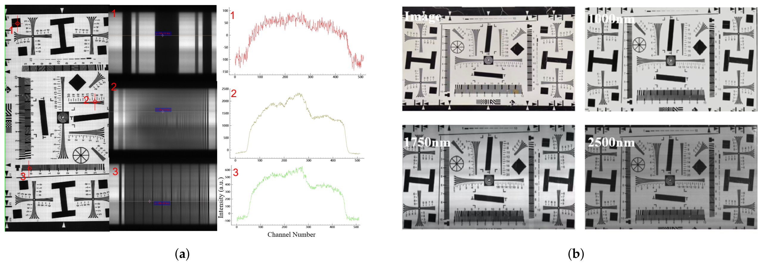
Laboratory imaging was conducted using a USAF resolution target, as illustrated in Figure 16. The spectral response maps in Figure 16a show that the system response peaks near the blaze wavelength and remains relatively flat across the operational band, conforming to the efficiency envelope of the reflective grating. No observable geometric distortion or coordinate shift is visible in the spatial dimension. Furthermore, the sharp feature contours and low background noise levels confirm a high SNR within the SWIR band, demonstrating robust spatio-spectral stability and achieving a measured spatial resolution of 2.5 μ m .
Single-wavelength images corresponding to 1000 nm , 1750 nm , and 2500 nm were subsequently extracted based on their channel indices, as presented in Figure 16b. These individual wavebands maintain distinct spatial boundaries and excellent spatial–spectral consistency. The instrument line shape (ILS) remains stable across the entire spectrum without anomalous broadening. Ultimately, results from the CCD-aided verification path confirm superior spectral imaging quality at the DMD plane: both spectral smile and chromatic keystone are tightly restricted to within a single pixel, spectral columns are accurately mapped, and the overall spatial resolution and spectral consistency fully satisfy the design specifications.

3.3.2. Field Imaging Experiment

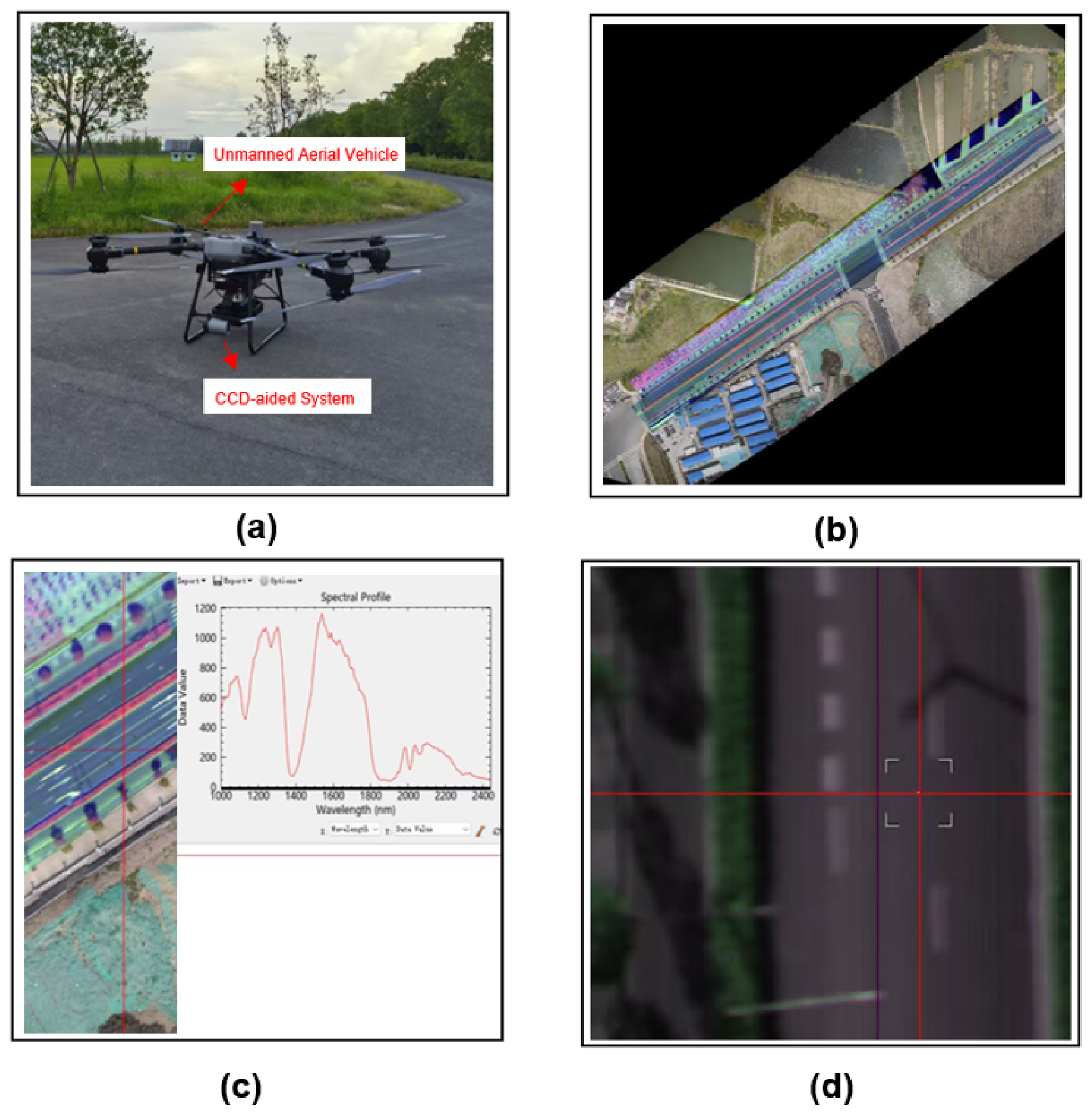
To verify the push-broom imaging stability under real-world operating conditions, the CCD-aided system was mounted on an unmanned aerial vehicle (UAV) for a multi-strip survey (Figure 17). The platform operated at an altitude of 100 m with a constant flight speed of 5 m / s , and the strip spacing was set to 20 m to maintain a 20 % overlap for mosaicking. Accounting for surface reflectance and the signal-to-noise ratio (SNR) of the SWIR detector, the single-frame exposure time was set to 19,000 μ s at an acquisition frequency of 50 Hz . The experimental results are presented in Figure 17a.
The raw spectral curves randomly extracted in Figure 17c indicate that the system sustains a high signal-to-noise ratio (SNR) under natural solar illumination. The precise capture of characteristic absorption peaks for typical features, such as vegetation, validates the system’s outstanding joint spatial–spectral acquisition capability. These results collectively demonstrate the reliability of the DMD-based front-end hyperspectral imaging module in accurately retrieving the spatial–spectral characteristics of targets. Specifically, they underscore the advantages of the proposed P-RG module in correcting spectral smile within the SWIR band. The accurate spatial–spectral mapping effectively eliminates the risk of cross-column crosstalk, ensuring the precise projection of broadband spectral columns onto the DMD plane. This established accuracy provides the essential physical prerequisite for high-precision joint spatial–spectral encoding and underscores the core scientific and engineering value of this work for single-pixel hyperspectral image reconstruction.
As clearly observed in the stitched hyperspectral imagery and the corresponding magnified views (Figure 17b,d), the lane markings, curbstone contours, and vegetation belt boundaries exhibit exceptional sharpness. The extended strip images demonstrate a smooth and natural transition during the push-broom mosaicking process, devoid of observable geometric distortion or scanning artifacts. This confirms that the front-end optical system maintains a superior modulation transfer function (MTF) across the entire field of view (FOV) and possesses remarkable stability against dynamic interference.

4. Discussion

This paper describes a DMD-scanning short-wave infrared (SWIR) hyperspectral imager built around a single-element detector, targeting the two obstacles that have kept such instruments out of low-cost deployment: the expense of large-format infrared focal plane arrays and the spectral smile that long entrance slits inevitably introduce. The core contribution is a three-dimensional analytical model for the P-RG compound dispersive element, derived from first principles for off-principal-plane incidence, which makes it possible to tune the prism apex angle and grating period until the smile contributions of the two elements cancel. Under this model, smile was held within one DMD pixel across the full 1000–2500 nm band.A CCD-assisted verification path was used to characterize the front-end optics independently of the DMD encoding stage. Monochromator calibration yielded 510 channels at 3.57 nm average resolution; an Ar-laser test at the single-element detector confirmed a 4.08 nm FWHM, in close agreement with the design prediction. Imaging experiments on a USAF target resolved features down to 2.5 μ m , and UAV field trials showed that the system holds its spatial–spectral mapping accuracy under natural illumination across multiple push-broom strips.
Reconstruction throughput remains bounded by current DMD switching rates and signal processing hardware, but the optical front end demonstrated in this work effectively addresses the persistent challenge of spectral smile. With smile and keystone both controlled at the sub-pixel level, the DMD plane provides a geometrically clean input for whatever encoding and reconstruction strategy is applied downstream.

Author Contributions

Conceptualization, J.Y. and H.Q.; methodology, Y.M. and X.P.; software, Y.M. and X.P.; validation, Y.M., X.P. and M.P.; formal analysis, Y.M.; investigation, Y.M. and X.P.; resources, J.Y. and H.Q.; data curation, Y.M.; writing—original draft preparation, Y.M.; writing—review and editing, Y.M., M.P., J.Y. and H.Q.; visualization, Y.M. and X.P.; supervision, J.Y. and H.Q.; project administration, J.Y. and H.Q.; funding acquisition, J.Y. and H.Q. All authors have read and agreed to the published version of the manuscript.

Funding

This research was funded by the National Natural Science Foundation of China, grant number 62375265; The Major Science and Technology Project of Shenzhen Municipality, grant number KJZD20230923113903008; and The Peacock Team Talent Special Program of Shenzhen Municipality, grant number KQTD20230301092838002. The APC was funded by the National Natural Science Foundation of China (62375265).

Institutional Review Board Statement

Not applicable.

Informed Consent Statement

Not applicable.

Data Availability Statement

The raw hyperspectral imaging data, optical system design parameters and wavelength calibration generated in this study are available from the corresponding author upon reasonable request. All processed analysis results and experimental measurements are presented in the main text of this article.

Acknowledgments

During the preparation of this manuscript, the authors used Google Gemini 3.5 for the purposes of translating Chinese text into English. The authors have reviewed and edited the output and take full responsibility for the content of this publication.

Conflicts of Interest

The authors declare no conflicts of interest.

References

  1. Goetz, A.F.; Vane, G.; Solomon, J.E.; Rock, B.N. Imaging spectrometry for Earth remote sensing. Science 1985, 228, 1147–1153. [Google Scholar] [CrossRef]
  2. Leitner, R.; Mairer, H.; Kercek, A. Real-time classification of polymers with NIR spectral imaging and blob analysis. Real-Time Imaging 2003, 9, 245–251. [Google Scholar] [CrossRef]
  3. Cheng, M.F.; Mukundan, A.; Karmakar, R.; Valappil, M.A.E.; Jouhar, J.; Wang, H.C. Modern trends and recent applications of hyperspectral imaging: A review. Technologies 2025, 13, 170. [Google Scholar] [CrossRef]
  4. Wilson, R.H.; Nadeau, K.P.; Jaworski, F.B.; Tromberg, B.J.; Durkin, A.J. Review of short-wave infrared spectroscopy and imaging methods for biological tissue characterization. J. Biomed. Opt. 2015, 20, 030901. [Google Scholar] [CrossRef]
  5. Vaughan, R.G.; Hook, S.J.; Calvin, W.M.; Taranik, J.V. Surface mineral mapping at Steamboat Springs, Nevada, USA, with multi-wavelength thermal infrared images. Remote Sens. Environ. 2005, 99, 140–158. [Google Scholar] [CrossRef]
  6. Bhan, R.K.; Dhar, V. Recent infrared detector technologies, applications, trends and development of HgCdTe based cooled infrared focal plane arrays and their characterization. Opto-Electron. Rev. 2019, 27, 174–193. [Google Scholar] [CrossRef]
  7. Gunapala, S.D.; Bandara, S.V.; Liu, J.K.; Mumolo, J.M.; Ting, D.Z.; Hill, C.J.; Nguyen, J.; Simolon, B.; Woolaway, J.; Wang, S.C.; et al. 1024 × 1024 format pixel co-located simultaneously readable dual-band QWIP focal plane array. Infrared Phys. Technol. 2005, 46, 285–293. [Google Scholar]
  8. Szajewski, K.; Szajewska, A.; Urbaś, S.; Więcek, B. Review on infrared single-pixel imaging. Opto-Electron. Rev. 2025, 33, e154306. [Google Scholar] [CrossRef]
  9. Gibson, G.M.; Johnson, S.D.; Padgett, M.J. Single-pixel imaging 12 years on: A review. Opt. Express 2020, 28, 28190–28208. [Google Scholar] [CrossRef]
  10. Studer, V.; Bobin, J.; Chahid, M.; Mousavi, H.S.; Candes, E.; Dahan, M. Compressive fluorescence microscopy for biological and hyperspectral imaging. Proc. Natl. Acad. Sci. USA 2012, 109, E1679–E1687. [Google Scholar] [CrossRef] [PubMed]
  11. Zhang, Z.; Wang, X.; Zheng, G.; Zhong, J. Hadamard single-pixel imaging versus Fourier single-pixel imaging. Opt. Express 2017, 25, 19619–19639. [Google Scholar] [CrossRef]
  12. Horadam, K. Hadamard Matrices and Their Applications; Princeton University Press: Princeton, NJ, USA, 2012. [Google Scholar]
  13. Zhao, Z.; Yu, Z.; Qi, H.; Han, J.; Zhang, Y.; Bai, L.; Xiong, F. Redundant compressed single-pixel hyperspectral imaging system. Opt. Commun. 2023, 546, 129797. [Google Scholar] [CrossRef]
  14. Park, J.; Gao, L. Cascaded compressed-sensing single-pixel camera for high-dimensional optical imaging. PhotoniX 2024, 5, 37. [Google Scholar] [CrossRef]
  15. Dong, X.; Tong, G.; Song, X.; Xiao, X.; Yu, Y. DMD-based hyperspectral microscopy with flexible multiline parallel scanning. Microsyst. Nanoeng. 2021, 7, 68. [Google Scholar] [CrossRef] [PubMed]
  16. Wu, Y.; Mirza, I.O.; Arce, G.R.; Prather, D.W. Development of a digital-micromirror-device-based multishot snapshot spectral imaging system. Opt. Lett. 2011, 36, 2692–2694. [Google Scholar] [CrossRef]
  17. Zhang, X.; Yu, K.; Zhang, J. Study on imaging spectrometer with smile and keystone eliminated. Opt. Commun. 2017, 387, 245–251. [Google Scholar] [CrossRef]
  18. Yu, C.; Yang, J.; Wang, M.; Sun, C.; Song, N.; Cui, J.; Feng, S. Research on spectral reconstruction algorithm for snapshot microlens array micro-hyperspectral imaging system. Opt. Express 2021, 29, 26713–26723. [Google Scholar] [CrossRef]
  19. Texas Instruments. DLP® NIRscan™ Nano SDK User’s Guide (Rev. D); Technical Reference Manual; Texas Instruments: Dallas, TX, USA, 2015. [Google Scholar]
  20. Chen, J.; Yang, J.; Liu, J.; Liu, J.; Sun, C.; Li, X.; Bayanheshig; Cui, J. Optical design of a short-wave infrared prism-grating imaging spectrometer. Appl. Opt. 2018, 57, F8–F14. [Google Scholar] [CrossRef]
  21. Jemec, J.; Pernuš, F.; Likar, B.; Bürmen, M. Deconvolution-based restoration of SWIR pushbroom imaging spectrometer images. Opt. Express 2016, 24, 24704–24718. [Google Scholar] [CrossRef]
  22. Zhang, X.; Li, B.; Jiang, X.; Gu, G.; Li, H.; Wang, X.; Lin, G. Design of a prism-grating wide spectral range transmittance imaging spectrometer. Sensors 2023, 23, 5050. [Google Scholar] [CrossRef]
  23. Wu, C.J.; Yan, C.X. Imaging spectrometer optical design based on prism-grating-prism dispersing device. J. Appl. Opt. 2012, 33, 37–43. [Google Scholar]
Figure 1. (a) Schematic diagram of the spectrometer optical system; (b) Schematic diagram of the DMD-based SWIR hyperspectral imaging system.
Optics 07 00039 g001
Figure 2. Schematic diagram of the DLP4500 micromirror array arrangement and dimensions.
Optics 07 00039 g002
Figure 3. Sketch of the main light path through the P-RG dispersion model: (a) projection in the meridian plane; (b) projection in the sagittal plane.
Optics 07 00039 g003
Figure 4. Three-dimensional diffraction optical path of a chief ray from an arbitrary field angle at the grating.
Optics 07 00039 g004
Figure 5. Spectral line curvature at 1750 nm with the prism apex angle set to 0° (grating dispersion only).
Optics 07 00039 g005
Figure 6. Relationship curves for parameter optimization. (a) Grating period d versus S ( x ) and Smile ( λ ) at a fixed prism apex angle β = 10 ° ; (b) Prism apex angle β versus S ( x ) and Smile ( λ ) at a fixed grating period d = 16.7 μ m . The red diamonds indicate the optimal intersection points.
Optics 07 00039 g006
Figure 7. Error distribution diagram of the P-RG dispersive element model.
Optics 07 00039 g007
Figure 8. The P-RG type SWIR hyperspectral imager: (a) Optical layout of the system; (b) Photograph of the prototype based on a DMD and a single-pixel detector.
Optics 07 00039 g008
Figure 9. MTF curves at the DMD plane for typical wavelengths. (a) 1000 nm ; (b) 1750 nm ; (c) 2500 nm .
Optics 07 00039 g009
Figure 10. Spot diagrams at the DMD plane across the full spectral range. All dimensional units are in μm, and the “100%” value refers to the radius enclosing 100% of the ray energy. (a) Red: 1010 nm, Green: 1005 nm, Blue: 1000 nm; (b) Red: 1755 nm, Green: 1750 nm, Blue: 1745 nm; (c) Red: 2500 nm, Green: 2495 nm, Blue: 2490 nm.
Optics 07 00039 g010
Figure 11. Spectral smile (a) and keystone (b) distributions at 1000 nm, 1750 nm, and 2500 nm after P-RG compensation.
Optics 07 00039 g011
Figure 12. Optical layout for CCD-aided imaging verification.
Optics 07 00039 g012
Figure 13. Measured mercury lamp spectral image in the 1000–1530 nm wavelength range.
Optics 07 00039 g013
Figure 14. Monochromator-based spectral calibration and full-band spectral resolution characterization: (a) Wavelength-to-channel mapping relationship; (b) FWHM of a wavelength peak.
Optics 07 00039 g014
Figure 15. Measured Ar laser spectral line at the detector end (FWHM = 4.08 nm).
Optics 07 00039 g015
Figure 16. Hyperspectral imaging results of a resolution target: (a) reconstructed images and spectral profiles of different regions on the resolution test target; (b) single-wavelength images reconstructed at different spectral channels.
Optics 07 00039 g016
Figure 17. UAV-borne imaging experiment: (a) UAV-borne CCD-aided imaging system image; (b) stitched dual-strip orthorectified hyperspectral image; (c) raw hyperspectral data corresponding to randomly selected spatial pixels; (d) spatial magnified view of a randomly selected local region.
Optics 07 00039 g017
Table 1. Comparison of Single-pixel Detector and SWIR Area Array Detectors.
Detector TypeCutoff WavelengthPeak Detectivity (D*)QEApproximate Cost
Single-pixel
(G12180-130K)
2.7 μ m 10 11 10 12 >80%$1100
InGaAs Array 2.5 μ m 10 9 10 10 60–70%
(Non-uniform)
>$30,000
MCT Array 2.6 μ m 10 9 10 10 60–70%
(Non-uniform)
>$100,000
Table 2. Main technical specifications of the system.
ParameterSpecification
Operational waveband1000–2500 nm
Object-space numerical apertureF/2.5
Slit length/width 7.6 mm / 15 μ m
System magnification 1.315 ×
Grating groove density/diffraction order 60 lines / mm , m = 1
Prism apex angle/material β = 9.1 ° , SiO 2
Spectral resolution (design value)Better than 8 nm
Spectral line curvature (smile)< 5 μ m (<1 pixel)
Chromatic distortion (keystone)< 5 μ m (<1 pixel)
Table 3. Optical glass materials for each lens.
Lens1234567
MaterialHLAK3HZPK1HZBAF16HZK6HKF6HZK50HZF12
Lens8910111213
MaterialHZF12HZK50HKF6HZK6HZBAF16HLAK3
Table 4. Tolerance allocation results.
ComponentTolerance TypeParameter Value
Standard LensesPower (fringe @ 632.8 nm) ± 0.25
Thickness (mm) ± 0.0125
X/Y Surface decenter (mm) ± 0.02
X/Y Surface tilt (°) ± 0.0167
X/Y Element decenter (mm) ± 0.02
X/Y Element tilt (°) ± 0.0167
Radius of curvature (fringe) ± 2
Refractive index ± 0.0005
Abbe number ± 0.1
DMDImage surface decenter (mm) ± 0.05
Image surface tilt (°) ± 0.0167
P-RG composite elementElement decenter (mm) ± 0.02
P/G surface decenter (mm) ± 0.02
P/G surface tilt (°) ± 0.0167
Table 5. Monte Carlo analysis results (MTF at the Nyquist frequency).
Probability1000 nm1350 nm1700 nm2050 nm2400 nm2500 nm
98 % 0.43370.43220.46200.42120.30210.2597
90 % 0.55830.54660.56140.53010.35870.3176
80 % 0.71150.65410.68150.60930.48320.3604
50 % 0.77510.63160.70150.66350.50160.4528
Disclaimer/Publisher’s Note: The statements, opinions and data contained in all publications are solely those of the individual author(s) and contributor(s) and not of MDPI and/or the editor(s). MDPI and/or the editor(s) disclaim responsibility for any injury to people or property resulting from any ideas, methods, instructions or products referred to in the content.