Article

Ultra-Low Power All-Optically Tuned Hybrid Graphene Ultra Silicon-Rich Nitride Ring Resonator-Based Add-Drop Filter for DWDM Systems

1
Electrical Engineering/Telecommunications Option, Institute for Basic Sciences, Technology and Innovation, Pan African University, Nairobi P.O. Box 62000 00200, Kenya
2
School of Electrical and Electronic Engineering, Technical University of Kenya, Nairobi P.O. Box 52428 00200, Kenya
*
Author to whom correspondence should be addressed.
Optics 2022, 3(3), 287-303; https://doi.org/10.3390/opt3030027
Submission received: 18 July 2022 / Revised: 11 August 2022 / Accepted: 15 August 2022 / Published: 31 August 2022
(This article belongs to the Section Nonlinear Optics)

Abstract

:
This research work conducted a design and simulation of an ultra-low power all-optically tuned nonlinear ring resonator-based add-drop filter. The purpose of this study is to investigate a CMOS-compatible nonlinear material system for an optical filter with temperature resilience, polarization insensitivity, and fast and energy-efficient tunability. The all-optical tunability was achieved using an optical pump that photo-excites the high nonlinear Kerr effect in the device material system. A three-dimensional multiphysics approach was used, combining the electromagnetics and thermo-structural effects in the filter. Hybrid graphene on an ultra-rich silicon nitride ring resonator-based filter enabled the realization of an ultra-high tuning efficiency (0.275 nm/mW for TE mode and 0.253 nm/mW for TM mode) on a range of 1.55 nm and thermal stability of 0.11 pm/K. This work contributed to the existing literature by proposing (1) the integration of a high Kerr effect layer on a low loss, high index contrast, and two-photon absorption-free core material with an athermal cladding material system and (2) the use of a cross-section shape insensitive to polarization. Moreover, the tuning mechanism contributed to the realization of an all-optical on-chip integrable filter for Dense Wavelength Division Multiplexing systems in the less occupied L band.

1. Introduction

All-optical networks are the right response to the growing demand for larger bandwidth and higher reliability driven by IoT applications, power efficient datacenters, video-on-demand, and cloud-related technologies [1,2]. Dense Wavelength Division Multiplexing (DWDM) techniques are the key method employed in the implementation of all-optical networks, since they provide a very effective utilization of fiber bandwidth directly in the optical domain [3]. Electronics nodes maintain high costs and limit the capacity of the network. The use of all-optical components avoids optical-to-electrical and electrical-to-optical conversion steps. Additionally, this saves power used for cooling overheating electronic components and subsequently, increases the life cycle of components. All-optical tunable filters are thus key elements in DWDM systems to ensure the accurate wavelength selection without interfering with neighboring channels [4]. Compared to filters based on bulk optics, ring resonator-based tunable optical filters are good candidates to meet criteria such as cost and power efficiency, low loss, small size and thus large scale integrability in existing optical architectures [5]. Moreover, the devices present power and nonlinearity enhancement due to the capacity to build up light power stored locally in ring resonators at resonance [6,7].
The silicon photonics platform is the most widely used in photonic-integrated circuits due to its compactness, low optical loss, and compatibility with the CMOS manufacturing technique [8]. However, its main challenge, especially in tunable optical filters, is poor nonlinear effects, which lead to weak tuning performance. Its relatively low Kerr coefficient ( 4 × 10 18 m 2 W 1 ), in particular, puts a limit on the power tuning efficiency of on-chip silicon photonics’ devices.
Different tuning methods change the refractive index exploiting various phenomena in the material including thermo-optic [9,10], electro-optic [11,12,13,14,15], and all-optical effects [7,8,16]. Thermally tuned silicon photonic devices exploiting the high thermo-optic coefficient ( 1.8 × 10 4 / K) and two-photon absorption nonlinearities in the silicon experience limited tuning speed and high power consumption [17]. Electro-optically tuned devices are faster than the latter but still integrate electronic components to the chip, thus adding extra complexity and a potential source of overheating.
Significant research efforts have been devoted to the design and fabrication of innovative devices that alleviate the aforementioned drawbacks of silicon nonlinear photonics by incorporating novel high nonlinear materials while retaining the silicon platform for its low cost, large scale integration potential, mature fabrication process, and CMOS compatibility.
In the same vein, one of the most promising and effective material system is silicon-rich nitride. This material demonstrates low temperature sensitivity, low nonlinear losses, and two-photon absorption free behavior while maintaining CMOS-compatibility and broadband transparency spanning from visible to infrared wavelengths, though it has lower mode confinement than pure silicon ( n Si 3 N 4 = 2.1 , n Si = 3.4 ) [18]. To reach stronger Kerr nonlinear optical properties than in silicon-rich nitride and further increase the mode confinement i.e., reduce the device size, the silicon content can be increased. Studies have demonstrated that a Si:N ratio of 7:3 maximizes the Kerr nonlinearity and mode confinement ( n Si 7 N 3 = 3.1 ), and maintains a two-photon absorption(TPA) and free carrier absorption (FCA) free behavior at telecommunication wavelengths beyond 1200 nm. TPA in silicon waveguides causes light to attenuate and the performance of nonlinear processes to degrade at higher powers [19]. In the following, this work will interchangeably refer to this composition ( Si 7 N 3 ) as ultra silicon-rich nitride or to its abbreviation, USRN. This material possesses the highest linear refractive index ( n U S R N = 3.1 ) across the spectrum of silicon nitride compositions and a nonlinear refractive index that is several orders of magnitude greater than that of crystalline silicon and stoichiometric silicon nitride, while keeping compatibility with CMOS platforms [20] (Table 1).
This property grants USRN a high confinement of waves and high enhancement of nonlinearities due to its strong proportion of silicon and the ring resonators used to design the filter, respectively, while it inherits the absence of TPA at telecommunication wavelengths from silicon-rich nitride. These attributes make USRN an ideal material for manufacturing CMOS-compatible nonlinear optics of small size devices, particularly at small optical powers [21]. Indeed, USRN has already proven a wideband supercontinuum potential [22] and spectral broadening [23,24], parametric optical amplifiers with high gain [25], and soliton phenomena [26], due to its strong nonlinearities.
To further enhance the tunability efficiency of the photonic devices, graphene, a 2D hexagonal lattice layer of carbon atoms (Figure 1) has proven to be an outstanding material candidate to be integrated onto high optical confinement waveguides [8,29]. Graphene’s use in photonic and optoelectronic devices has increased thanks to its distinctive electronic and optical properties, including CMOS compatibility [30]. Its Fermi energy can be tuned significantly with relatively low energy required. The graphene integration on ultra silicon-rich nitride waveguides opens the way to the implementation of fast, reconfigurable, highly tunable, and power efficient nonlinear systems in Photonics -ntegrated Circuits (PICs) [31], owing to its high Kerr coefficient in the range of 10 13 10 7 m 2 /W, depending on the quality of graphene [8].
In this work, alternative cladding materials to classical silicon oxide for temperature resilience and a proper waveguide cross-section engineering for a polarization insensitive fourth-order ring resonator-based add drop filter were explored. As a result, a new material system, SiO 2 Si 7 N 3 C TiO 2 , where silicon and titanium oxides are used for under and upper cladding materials, respectively, on the one hand, while USRN and graphene are used as a Kerr nonlinear active medium, on the other hand, was deployed and investigated. Hence, by using the proposed innovative material system, this paper designed a fast all-optical tunable on-chip athermal device that takes advantage of the optical confinement, low loss, and TPA-free properties of USRN-based waveguides as well as the high optical nonlinearities of hybrid graphene integrated onto USRN. The simulation results reveal that the 25 GHz-all-optical filter is tunable on a range of 1.55 nm using a 28–33 mW power range. This provides a significant reference for further research in all-optical tunable devices, demonstrating the potential for high-speed and energy efficient tunable filter application in integrated all-optical DWDM systems.

2. Materials and Methods

In this section, the work describes the spectral and physical characteristics of the filter. The methodology to achieve the results is also developed.

2.1. Athermality and Polarization Sensitivity

The temperature-induced resonant wavelength shift in a microring resonator is given by [32]:
d λ d T = λ n g n e f f T + n e f f α s u b ,
where n g and α s u b are the group index of the waveguide and the coefficient of the thermal expansion (CTE) of the substrate, respectively. From (1), the athermal condition is fulfilled when n e f f T = n e f f α s u b , thus n e f f T has to be negative. This can be realized by using a cladding material, titanium oxide ( TiO 2 ) in the case of this work, with a negative thermo-optic coefficient.
Studies have demonstrated that polarization independence may be achieved by modifying the height-width ratio of the waveguide [33]. In this work, the geometrical parameters are optimized such that n e f f , T E = n e f f , T M and to allow a dual spatial modes operation for both TE and TM polarized signals. In addition, a critical radius was computed to minimize polarization rotation, bend losses, and induce stress that enhances polarization sensitivity and additional index shifts in the waveguide with the ring radius reduction.

2.2. Optical Properties of Graphene

The graphene’s chemical potential ( μ c ) is optically tuned by an optical pump that injects power in the structure of the filter. This alters the transmission characteristics of the filter by tuning the resonance of the filter at room temperature [34]. 2D materials such as graphene are usually characterized by their complex surface conductivity [35] as a result of contributions from intraband and interband transitions according to the Kurbo model [28]
σ ( ω , Γ , μ c , T ) = σ i n t r a ( ω , Γ , μ c , T ) + σ i n t e r ( ω , Γ , μ c , T ) .
The intra- band term is written as
σ i n t r a = i e 2 k B T π 2 ( ω + i 2 Γ ) μ c k B T + 2 l n ( e μ c k B T + 1 ,
while the inter-band term is given by
σ i n t e r = i e 2 4 π l n 2 | μ c | ( ω + i 2 Γ ) 2 | μ c | + ( ω + i 2 Γ ) ,
where ω , Γ , μ c , T, e, , and k B , are the angular frequency, scattering rate, chemical potential, temperature, electron charge, reduced Planck constant, and Boltzmann constant, respectively.
The permittivity can be deduced from the above using
ε ( ω , Γ , μ c , T ) = ε r + i σ ( ω , Γ , μ c , T ) ε 0 ω Δ .
ε 0 , ε r , Δ represent the vacuum permittivity, the relative permittivity, and the layer thickness, respectively. The complex refractive index can directly be deduced from (5) as n + i k = ε ( ω , Γ , μ c , T ) , where n and k are its real and imaginary parts, respectively.
As illustrated in Figure 2 when the optical energy pump is close to the transition point between intraband and interband regions, the incident photons excites electrons through the interband absorption process. As a result of the high absorption, the graphene layers become a highly lossy medium. With increasing incident energy, the absorption reaches a peak value equivalent to half the photon energy, and all the graphene electron states would be filled. According to the Pauli blocking principle, beyond that point, no interband transition is allowed. Therefore, the graphene layers behave like a transparent thin sheet [36]. The step change region (0.2 eV < μ c < 0.64 eV), suitable for the tuning process, corresponds to a significant change of the conductivity and thereby the refractive index of graphene (Figure 2).

2.3. Nonlinear Effects Induced Refractive Index Change
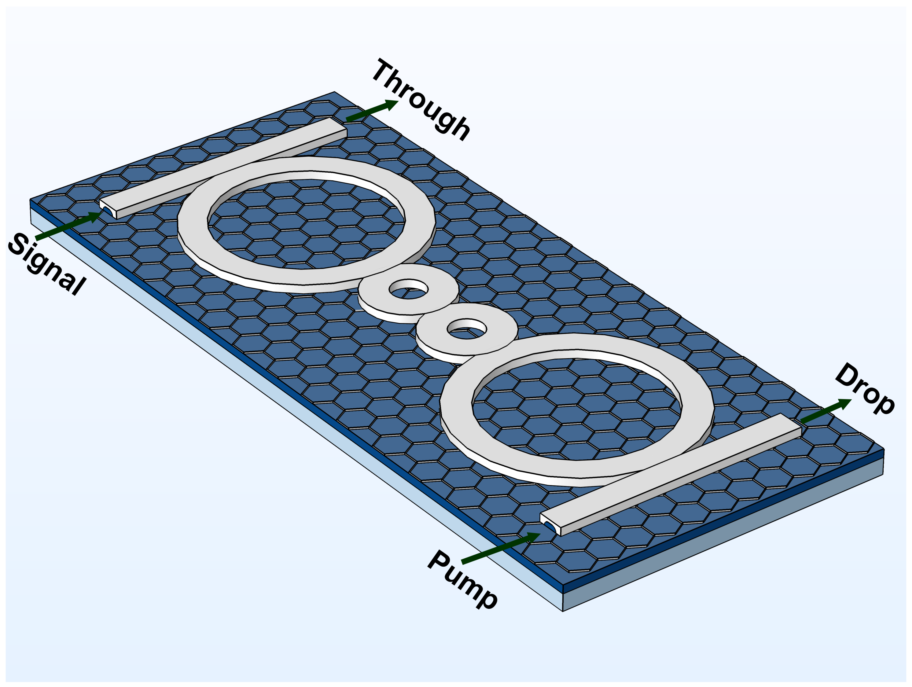
Two optical sources were used to couple the signal and the pump waves in the input and add ports of the filter waveguide, respectively (Figure 1). The pump and the signal are around the same resonant wavelength but differentiated based on propagation direction, each coupled to a separate port. Hence, under the reciprocity operation principle, with ω s i g n a l ω p u m p = ω 0 , it is assumed that the two beams have approximately similar energy distribution and therefore experience the same coupling, loss, and confinement. The pump is considered as a short pulse with enough power and energy to excite the Kerr nonlinearity. This ensures that the pump is only responsible for nonlinear effects, since the signal is much weaker. Therefore, nonlinearities are generated in graphene and USRN core material through the Kerr effect. This involves a shift in the refractive index as a function of the light intensity using mW level powers due to power and nonlinearities enhancement in the highly confining ring resonators [37].
The work described the nonlinear effects in URSN microring resonators and attempted to determine the pump-induced resonant wavelength shift in microrings [38] using nonlinear coupled mode theory(NCMT). The nonlinear wavelength shift in the ring resonator-based filter is introduced as a perturbation of the linear coupled mode equations, as expressed by the following [39]:
d a 1 m d t = ( j ω 1 Δ ω N L p γ i γ 0 γ N L p ) a 1 m j μ 1 a 2 m j μ 0 s i , d a 2 m d t = ( j ω 2 Δ ω N L p γ i γ N L p ) a 2 m j μ 1 a 1 m j μ 2 a 3 m , d a N 1 m d t = ( j ω N 1 Δ ω N L p γ i γ N L p ) a N 1 m j μ N 2 a N 2 m j μ N 1 a N m d a N m d t = ( j ω N Δ ω N L p γ i γ N γ N L p ) a N m j μ N 1 a N 1 m ,
where m = s , p , denotes signal (s) and pump (p) inputs, respectively. μ i ( 1 i N 1 ) represent the coupling coefficients between microrings i and i + 1 . N corresponds to the order of the filter, which is also equivalent to the number of ring resonators. In (6), γ i takes into account the intrinsic and coupling losses between the ring resonators. The decay rates γ 0 and γ N , computed as γ 0 = μ 0 2 / 2 and γ N = μ N 2 / 2 , respectively, consider the intrinsic and coupling losses between the outer microrings and the bus waveguides [5].
ω i and a i denote the resonant frequency and the wave amplitude related to the microring i, respectively.
Due to the strong Kerr nonlinearity in graphene and USRN, it is assumed that the Kerr nonlinearity is the main source of the refractive index change Δ n N L p , given by
Δ n N L p = n 2 K e r r I p
and the nonlinear Kerr parameter is given by
γ N L p = 2 π n 2 λ A e f f ,
where n 2 is the Kerr coefficient of graphene. I p is the pump intensity coupled into the filter device.
A change in effective refractive induces a resonant frequency shift computed using perturbation theory as
Δ ω N L p = V n Δ n N L p | E | 2 d V n 2 | E | 2 d V ,
where V is the volume of the ring resonator and E the electric field intensity confined in the ring.
The transfer functions are derived from the solutions to nonlinear coupled mode equations under the assumption of harmonic input wave excitation and harmonic wave amplitudes, that is, s i e j ω t and a i e j ω t , respectively. Thus,
H t = s t s i = 1 j μ 0 a 1 s i = 1 μ 0 2 s + γ 0 + μ 1 2 s + μ 2 2 s + μ N 1 2 s + γ N ,
H d = s d s i = j μ N a N s i = ( j ) N + 1 ( μ 0 μ 1 μ 2 μ N ) C N ( s ) ,
where H t , H d are the transfer functions at through and drop ports, respectively, while s i , s t , s d are signals at the input, through, and drop ports, respectively.
The complex centered frequency s around the resonant frequency ω i is written as s = j ( ω ω i ) + γ i + Δ ω N L p + γ N L p and C N ( s ) corresponds to the expression of the denominator in the through port transfer function.

2.4. Methodology

A space design exploration for the filter was conducted to relate the targeted spectral parameters of the DWDM frequency grid recommendation [40] to the physical parameters of the filter. This resulted in the determination of optimal physical parameters of the filter, such as the cross-section dimensions, the critical ring radius, and gap distances (Figure 1). A full vectorial finite element tool in COMSOL Multiphysics was used to analyze modes on the waveguide cross-section, and ensured that our design can transmit arbitrarily quasi-TE and quasi-TM fundamental modes with a maximal bend radius to keep optimal confinement of the fields in the filter waveguides.
The research took into account a variety of physical aspects of the analysis (combination of electromagnetics, structural mechanics, and heat transfer) to simulate real-world operational conditions in on-chip photonics devices. To investigate such effects, various modules in the COMSOL Multiphysics software such as Wave Optics, Heat Transfer in Solids, and Solid Mechanics physics, coupled to thermal expansion multiphysics, respectively, were incorporated in the model. Under the slowly varying envelop approximation of the electric field, the electromagnetic waves’ propagation in the device was simulated by using the Electromagnetic Wave Beam Envelope (EWBE) interface in COMSOL. Simulations were carried on an ideal new material system to come up with an all-optical filter with tunable, athermal, and polarization-insensitive features in compliance with add-drop filters in a DWDM network. The model was continuously updated according to a performance evaluation of the filter based on the targeted filter specifications prior to the validation of the final results. S-parameters’ simulation results were compared with transfer functions of the filter as a result of solving nonlinear coupled mode equations in the Matlab software. Based on the optical properties of graphene, a tuning range of the optical power pump was determined to efficiently tune the device.

3. Results and Discussion

The designed filter configuration was chosen for this device with a rib height of 50 nm. The rib gives the advantage of reducing losses [8]. Given the dimensions that allow a temperature, polarization stability, and highly confined modes in the core of the filter waveguides, this step aims to determine the effective index of the group index as well as a critical bending radius with maximal mode confinement in the filter.
Based on this analysis, the results in Table 2, an optimized waveguide with athermality and polarization insensitivity features, were achieved. A rib waveguide with a rounded corner-cross-section enabled a high mode confinement in the waveguide (Figure 3). The core size and the cladding thickness determines the confinement factor. The optimal values for cladding thickness to realize an athermal behavior and a high confinement for quasi-fundamental TE and TM modes are given in Figure 3 and Table 3. An optimal ring radius of 9 μ m that prevents polarization rotation was determined with bending losses of 1.65 × 10 5 dB/cm, using a Finite Element mode solver.
This study designed a structure, which is composed of four microring resonators and two bus waveguides. The outer ring resonators have a radius of R 1 = 9   μ m and the two inner smaller rings have a radius of R 2 = 3   μ m each to realize the Vernier effect. The gap distance between the outer rings and bus waveguides is denoted by d 0 = d 4 = 120 nm. Similarly, the distance between outer rings and the inner smaller rings is denoted by d 1 = d 3 = 129 nm, while the distance between the smaller rings is d 2 = 90 nm (Figure 1).
A waveguide with a rounded-corner rectangular cross-section (Figure 1) enabled us to achieve athermality and polarization insensitivity in a single mode operation. The TE and TM fundamental modes’ effective indices in both polarization modes are very close, as assessed by simulation results in Table 2. The field confinement factors for both modes in Table 2 show a good mode confinement as confirmed by Figure 4 and Figure 5. Due to the judicious selection of waveguide parameters, the modes are well confined in the core of the waveguide (Figure 6).
This research work targeted a maximal 1 dB-attenuation in the passband, a linewidth of 0.2 nm (25 GHz) centered on λ = 1581.5 nm in the 1565–1625 nm band. Based on the geometry shown in Figure 1, a fourth-order ring resonator-based add-drop filter was designed. The 3D multiphysics simulation results in Figure 7, Figure 8, Figure 9, Figure 10, Figure 11 and Figure 12 present the spectral thermal and tuning characteristics of the filter. The drop and through ports responses computed from nonlinear coupled mode equation solutions and the S-parameters from the simulation of the electromagnetic wave propagation at corresponding ports are plotted together in Figure 7. The study simulated this phenomenon using the Electromagnetic Wave and Beam Envelope Method, assuming a slowly varying envelope of the electric/magnetic field and propagation over distances that are many wavelengths long. The simulations were performed on a fourth-order serially coupled microring filter. The simulation results at T = 298 K for the TE mode (a slight difference is observed in TM mode) are as follows: FWHM = 25 GHz (0.2 nm) around the center wavelength of 1581.52 nm, FSR = 35 nm, Q = 5933, Finesse = 134 and a minimum attenuation in the stop band = 139 dB. A slight detune of the resonant wavelength towards the design wavelength (1581.5 nm) was observed. The FSR has been expounded using the Vernier effect, as demonstrated in the suggested topology (Figure 1) and the resulting spectrum in Figure 9. In this process, apodized coupling coefficients were used to obtain a maximally flat drop port response in the passband, due to the finite length state of the number of microrings, to prevent large ripples that can appear in the passband. This results in a filter with a flat-top response that is compatible with the desired application. The slight difference in results between the two methods can be explained by the inaccuracy in the computation of nonlinearities in NCMT and coupling losses all along with the filter. In FEM simulations, the drop port transmission response showed a 0.91 dB loss in the passband and a less noticeable notch behavior in the through port response (Figure 7).
The signal coupled into the filter at resonance exits at the drop port. The fields are well confined in the core materials and show low coupling losses (Figure 10).
To tune the resonant wavelength to the design wavelength (1581.5 nm) or to a different channel, an optical pump injects a control signal power through the add port (Figure 1). The effective index change as a function of the injected pump power enabled the determination of a tuning power range of 28–34 mW through a parametric sweep study (Figure 8).
The resonant wavelength was tuned thanks to a parameter sweep on the injected pump power. The filter reached a high tuning efficiency of 0.275 nm/mW in the TE mode over a tunability range of 1.55 nm (Figure 9). However, there is a difference in tuning performance between TE and TM modes as predicted by the results displayed in Figure 8. A difference in tunability in TM mode where the tunability range of 1.068 nm and the tunability efficiency ( 0.253 nm/mW) are less than in the case of TE polarized signals, but yet do not alter the filter performance for DWDM systems, where identified. This is an outstanding result consequent to the new system material combining a high confinement core material with a high nonlinear coefficient coated with a graphene layer to enhance the Kerr effect even more in the device due to high Kerr nonlinearity. The ring resonators used to realize the filter not only enabled the realization of an ultra compact device but also an ultra highly efficient tuning and energy efficient device due to the enhancement of the fields and nonlinearities in the structure at ultra-low power levels.
The study then assumed two situations, where the part upon which the device is integrated experiences heating from the nearby components and a temperature variation due to modification of the ambient temperature. This imposes a temperature variation across the filter that will heat and may distort the spectral characteristics of the filter. The temperature distribution for the first case, as an illustration, is shown in Figure 11 and the corresponding von Mises stress profile is plotted in Figure 12. The stress profile in Figure 12 exhibited slightly high values in the intersection of different layers, essentially due to differences of coefficients of thermal expansions of the different layers and at highly curved sections of the filter. Both temperature and von Mises stress profiles’ effects on the filter are negligible. The temperature variation was investigated using a parametric sweep study in the simulation. The model first simulated the thermo-structural problem, and then it simulated the electromagnetic wave propagation on the deformed state. When a temperature change occurs in the device (Figure 11) from 298 K (dT = 0) to 400 K (dT = 102) in both situations, slight shifts of 0.09 pm/K (Figure 13) and 0.11 pm/K (Figure 14), respectively, occurs in the resonant wavelength in TE mode but is still acceptable for the filter to operate efficiently in DWDM systems with such a good athermal behavior. The same simulations performed in TM mode lead to slightly similar conclusions.
The main performance characteristics of the designed filter in this work are summarized as follows: the study achieved an ultra-high tuning efficiency of 0.275 nm/mW and 0.253 nm/mW for TE and TM modes, respectively, ensuring an ultra-low power consumption, a Full-wave at Half Maximum bandwidth of 25 GHz, a high free spectral range of 35 nm, a quality factor of 5933, a finesse of 134, an extinction ratio of 139, and thermal stability of 0.11 pm/K. This filter was designed for DWDM systems. A tuning range of 1.55 nm using pump power in the 28–34 mW range was reached. The use of a multiphysics approach in the simulation of this device offers a unique advantage to create conditions close to the real operational conditions of the device in a Photonic Integrated Circuit (PIC) setting. The fabrication imperfections may represent a slight difference from the experimental results. Additionally, the use of an all-optical tuning mechanism assumes an infinite tuning speed but the latter is limited by the recombination time of the carriers in the material system of the device. In comparison with recent experimental results, a CMOS-compatible hybrid titanium dioxide/silicon-rich nitride planar ring resonator that is both polarization insensitive and athermal with a thermal drift of the resonance wavelength <1.5 pm/K, was designed [41]. Another experimental attempt designed a diamond micro-disk resonator integrated with a silicon-on-insulator waveguide [7]. In this device, continuous resonant wavelength tuning across a 450 pm range using a mW level optical pump was achieved, exploiting the thermo-optic effect in silicon. Another experimental attempt with quite a similar tuning efficiency though on a shorter range and with a slightly complex structure based on double opto-mechanical microring resonators assisted Mach-Zehnder interferometer structure is reported with a tuning efficiency of 0.277 nm/mW, from 1550.09 nm to 1550.60 nm with a small passband ripple of 1 dB [16]. In that line, combined electro-mechanical and thermo-optic effects in a silicon opto-mechanical microring resonator (MRR)-based microwave filter experimentally demonstrated a continuous tunability of the central frequency on a range of 13 GHz (0.1 nm) with pump power lower than −2.5 dBm (0.56 mW) [42].

4. Conclusions

This work was concerned with the design and analysis of a tunable all-optical add-drop ring resonator-based filter. The filter associates the advantages of strong Kerr nonlinearity and high mode confinement of the hybrid graphene ultra silicon-rich nitride material system, which can handle arbitrarily polarized signals with high thermal stability. Keeping in mind the characteristics of an add-drop filter for DWDM systems, the designed filter is one of its kind in the sense that it combines a flat-top response in the passband, athermality, polarization insensitivity, and fast and energy-efficient tuning. Additionally, the device is ultra-compact and CMOS-compatible, presenting the possibility of very large-scale integration potential. The high tunability performed at ultra-low powers is not only due to the strong Kerr nonlinearity in the hybrid material system used but also to the inherent power built-up capacity of ring resonators that enables the realization of important nonlinearities effects at mW power levels. Although the opto-mechanical effect exhibits a competitive tuning efficiency, its range, as well as its tuning speed, are smaller compared to those achieved in this study, exploiting the Kerr nonlinear effect. This work paves the way for ultrafast tuning and energy-efficient operation inherent to the all-optical nature of the used mechanism and to the resonant nature of ring resonators. Additionally, it contributes to the realization of future ultra-fast and energy-efficient all-optical tunable devices such as filters and modulator switches for DWDM networks.

Author Contributions

Conceptualization, F.R., S.M. and E.A.; methodology, F.R.; software, F.R.; validation, F.R.; formal analysis, F.R.; investigation, F.R.; writing—original draft preparation, F.R.; writing—review and editing, F.R., S.M. and E.A.; visualization, F.R.; supervision, S.M. and E.A. All authors have read and agreed to the published version of the manuscript.

Funding

This research was funded by the African Union Commission through a scholarship and The APC was partially funded by the same institution.

Institutional Review Board Statement

Not applicable.

Informed Consent Statement

Not applicable.

Data Availability Statement

Not applicable.

Acknowledgments

Filston Rukerandanga wishes to acknowledge the African Union Commission for their scholarship.

Conflicts of Interest

The authors declare no conflict of interest.

Sample Availability

Samples of the compounds are available from the authors.

Abbreviations and Nomenclature

The following abbreviations are used in this manuscript:
TETranverse Electric
TMTransverse Magnetic
DWDMDense Wavelength Division Multiplexing
CMOSComplementary metal-oxide-semiconductor
IoTInternet of Things
SiSilicon
Si 3 N 4 Silicon-Rich Nitride
Si 7 N 3 or URSRNUltra Silicon-Rich Nitride
TPATwo-Photon Absorption
FCAFree Carrier Absorption
PICPhotonic-Integrated Circuits
CGraphene
SiO 2 Silicon Oxide
TiO 2 Titanium Oxide
CTECoefficient of Thermal Expansion

References

  1. Karimi, R.; Koohi, S.; Tinati, M.; Hessabi, S. A thermally-resilient all-optical network-on-chip. Microelectron. Reliab. 2019, 99, 74–86. [Google Scholar] [CrossRef]
  2. Vale, V.; Almeida, R.C., Jr. Power, routing, Modulation Level and Spectrum Assignment in all-optical and elastic networks. Opt. Switch. Netw. 2019, 32, 14–24. [Google Scholar] [CrossRef]
  3. Rani, A.; Bhamrah, M.S.; Dewra, S. Performance evaluation of the dense wavelength division multiplexing system using reconfigurable optical add/drop multiplexer based on digital switches. Opt. Quantum Electron. 2020, 52, 480. [Google Scholar] [CrossRef]
  4. Dai, T.; Shen, A.; Wang, G.; Wang, Y.; Li, Y.; Jiang, X.; Yang, J. Bandwidth and wavelength tunable optical passband filter based on silicon multiple microring resonators. Opt. Lett. 2016, 41, 4807–4810. [Google Scholar] [CrossRef]
  5. Vey Van, K.A. Optical Microring Resonators: Theory, Techniques, and Applications; CRC Press: Boca Raton, FL, USA; Taylor et Francis Group: Abingdon, UK, 2018; p. 250. [Google Scholar] [CrossRef]
  6. Thomson, D.; Zilkie, A.; Bowers, J.E.; Komljenovic, T.; Reed, G.T.; Vivien, L.; Marris-Morini, D.; Cassan, E.; Virot, L.; Fédéli, J.M.; et al. Roadmap on silicon photonics. J. Opt. 2016, 18, 073003. [Google Scholar] [CrossRef]
  7. Hill, P.; Klitis, C.; Guilhabert, B.; Sorel, M.; Gu, E.; Dawson, M.D.; Strain, M.J. All-optical tuning of a diamond micro-disk resonator on silicon. Photonics Res. 2019, 8, 318–324. [Google Scholar] [CrossRef]
  8. Ooi, K.J.; Leong, P.C.; Ang, L.K.; Tan, D.T. All-optical control on a graphene-on-silicon waveguide modulator. Sci. Rep. 2017, 7, 12748. [Google Scholar] [CrossRef]
  9. Bahadori, M.; Nikdast, M.; Rumley, S.; Dai, L.Y.; Janosik, N.; Van Vaerenbergh, T.; Gazman, A.; Cheng, Q.; Polster, R.; Bergman, K. Design Space Exploration of Microring Resonators in Silicon Photonic Interconnects: Impact of the Ring Curvature. J. Light. Technol. 2018, 36, 2767–2782. [Google Scholar] [CrossRef]
  10. Manganelli, C.L.; Pintus, P.; Gambini, F.; Fowler, D.; Fournier, M.; Faralli, S.; Kopp, C.; Oton, C.J. Large-FSR Thermally Tunable Double-Ring Filters for WDM Applications in Silicon Photonics. IEEE Photonics J. 2017, 9, 1–10. [Google Scholar] [CrossRef]
  11. Ahmed, A.N.R.; Shi, S.; Zablocki, M.; Yao, P.; Prather, D.W. Tunable hybrid silicon nitride and thin-film lithium niobate electro-optic microresonator. Opt. Lett. 2019, 44, 618–621. [Google Scholar] [CrossRef]
  12. Dubray, O.; Abraham, A.; Hassan, K.; Olivier, S.; Marris-Morini, D.; Vivien, L.; O’Connor, I.; Menezo, S. Electro-Optical Ring Modulator: An Ultracompact Model for the Comparison and Optimization of p-n, p-i-n, and Capacitive Junction. IEEE J. Sel. Top. Quantum Electron. 2016, 22, 89–98. [Google Scholar] [CrossRef]
  13. Li, S.; Chen, W.; Wang, P.; Fu, Q.; Zhang, J.; Zhang, B.; Dai, T.; Wang, Y.; Yang, J. Bandwidth-tunable optical passband filter based on graphene-silicon waveguide. Opt. Commun. 2018, 426, 206–211. [Google Scholar] [CrossRef]
  14. Han, H.; Xiang, B. Simulation and analysis of electro-optic tunable microring resonators in silicon thin film on lithium niobate. Sci. Rep. 2019, 9, 6302. [Google Scholar] [CrossRef]
  15. Ahmed, N.; Nelan, S.; Shi, S.; Yao, P.; Mercante, A.; Prather, D. Sub-volt electro-optical modulator on thin-film lithium niobate and silicon nitride hybrid platform. Opt. Lett. 2020, 45, 1112–1115. [Google Scholar] [CrossRef]
  16. Chen, M.; Liu, L.; Xu, L.; Ye, M.; Jin, X.; Yu, Z. On-Chip all-optical tunable filter with high tuning efficiency. IEEE Photonics J. 2020, 12, 1–10. [Google Scholar] [CrossRef]
  17. Wang, J.; Fan, L.; Varghese, L.T.; Shen, H.; Xuan, Y.; Niu, B.; Qi, M. A theoretical model for an optical diode built with nonlinear silicon microrings. J. Light. Technol. 2013, 31, 313–321. [Google Scholar] [CrossRef]
  18. Meng, Y.; Lu, R.; Shen, Y.; Liu, Y.; Gong, M. Ultracompact graphene-assisted ring resonator optical router. Opt. Commun. 2017, 405, 73–79. [Google Scholar] [CrossRef]
  19. Tu, Z.; Chen, D.; Hu, H.; Gao, S.; Guan, X. Characterization and Optimal Design of Silicon-Rich Nitride Nonlinear Waveguides for 2 μm Wavelength Band. Appl. Sci. 2020, 10, 8087. [Google Scholar] [CrossRef]
  20. Choi, J.W.; Sohn, B.U.; Chen, G.F.; Ng, D.K.; Tan, D.T. Correlated photon pair generation in ultra-silicon-rich nitride waveguide. Opt. Commun. 2020, 463, 125351. [Google Scholar] [CrossRef]
  21. Tan, D.T.H.; Ng, D.K.T.; Choi, J.W.; Sahin, E.; Sohn, B.U.; Chen, G.F.R.; Xing, P.; Gao, H.; Cao, Y. Nonlinear optics in ultra-silicon-rich nitride devices: Recent developments and future outlook. Adv. Phys. X 2021, 6, 1905544. [Google Scholar] [CrossRef]
  22. Wang, T.; Ng, D.K.; Ng, S.K.; Toh, Y.T.; Chee, A.K.; Chen, G.F.; Wang, Q.; Tan, D.T. Supercontinuum generation in bandgap engineered, back-end CMOS compatible silicon rich nitride waveguides. Laser Photonics Rev. 2015, 9, 498–506. [Google Scholar] [CrossRef]
  23. Choi, J.W.; Chen, G.F.; Ng, D.; Ooi, K.J.; Tan, D.T. Wideband nonlinear spectral broadening in ultra-short ultra-silicon rich nitride waveguides. Sci. Rep. 2016, 6, 27120. [Google Scholar] [CrossRef]
  24. Sahin, E.; Ooi, K.J.; Chen, G.; Ng, D.K.; Png, C.; Tan, D.T. Enhanced optical nonlinearities in CMOS-compatible ultra-silicon-rich nitride photonic crystal waveguides. Appl. Phys. Lett. 2017, 111, 121104. [Google Scholar] [CrossRef]
  25. Ooi, K.; Ng, D.; Wang, T.; Chee, A.; Ng, S.; Wang, Q.; Ang, L.; Agarwal, A.; Kimerling, L.; Tan, D. Pushing the limits of CMOS optical parametric amplifiers with USRN: Si7N3 above the two-photon absorption edge. Nat. Commun. 2017, 8, 13878. [Google Scholar] [CrossRef] [PubMed]
  26. Dong, Z.; Si, J.; Yu, X.; Deng, X. Optical spatial differentiator based on subwavelength high-contrast gratings. Appl. Phys. Lett. 2018, 112, 181102. [Google Scholar] [CrossRef]
  27. Krückel, C.J.; Fülöp, A.; Klintberg, T.; Bengtsson, J.; Andrekson, P.A.; Víctor Torres-Company. Linear and nonlinear characterization of low-stress high-confinement silicon-rich nitride waveguides. Opt. Express 2015, 23, 25827–25837. [Google Scholar] [CrossRef]
  28. Vorobev, A.S.; Bianco, G.V.; Bruno, G.; D’Orazio, A.; O’Faolain, L.; Grande, M. Tuning of Graphene-Based Optical Devices Operating in the Near-Infrared. Appl. Sci. 2021, 11, 8367. [Google Scholar] [CrossRef]
  29. Ataloglou, V.G.; Christopoulos, T.; Kriezis, E.E. Nonlinear coupled-mode-theory framework for graphene-induced saturable absorption in nanophotonic resonant structures. Phys. Rev. A 2018, 97, 063836. [Google Scholar] [CrossRef]
  30. Conteduca, D.; Dell’Olio, F.; Ciminelli, C.; Armenise, M. Resonant graphene-based tunable optical delay line. IEEE Photonics J. 2015, 7, 1–9. [Google Scholar] [CrossRef]
  31. Demongodin, P.; El Dirani, H.; Lhuillier, J.; Crochemore, R.; Kemiche, M.; Wood, T.; Callard, S.; Rojo-Romeo, P.; Sciancalepore, C.; Grillet, C.; et al. Ultrafast saturable absorption dynamics in hybrid graphene/Si3N4 waveguides. APL Photonics 2019, 4, 076102. [Google Scholar] [CrossRef]
  32. Namnabat, S.; Kim, K.J.; Jones, A.; Himmelhuber, R.; DeRose, C.T.; Trotter, D.C.; Starbuck, A.L.; Pomerene, A.; Lentine, A.L.; Norwood, R.A. Athermal silicon optical add-drop multiplexers based on thermo-optic coefficient tuning of sol-gel material. Opt. Express 2017, 25, 21471–21482. [Google Scholar] [CrossRef]
  33. Venghaus, H. Wavelength Filters in Fibre Optics; Springer Series in Optical Sciences; Springer: Berlin/Heidelberg, Germany, 2007. [Google Scholar] [CrossRef]
  34. Deng, G.; Zhao, T.; Yin, Z.; Yang, J. Bandpass filter based on comb shaped graphene nanoribbons. OSA Contin. 2019, 2, 2614–2622. [Google Scholar] [CrossRef]
  35. Čtyrokỳ, J.; Petráček, J.; Kwiecien, P.; Richter, I.; Kuzmiak, V. Graphene on an optical waveguide: Comparison of simulation approaches. Opt. Quantum Electron. 2020, 52, 149. [Google Scholar] [CrossRef]
  36. Wang, Y.; Lei, L.; Zang, J.; Dong, W.; Zhang, X.; Xu, P. High Efficiency Electro-Optic Modulation in a Graphene Silicon Hybrid Tapered Microring Resonator. IEEE Access 2021, 9, 87869–87876. [Google Scholar] [CrossRef]
  37. Liu, L.; Liao, S.; Xue, W.; Yue, J. Tunable all-optical microwave filter with high tuning efficiency. Opt. Express 2020, 28, 6918–6928. [Google Scholar] [CrossRef]
  38. Abdullah, F.; Alani, F.; Yaqoub, Y.; Hamdan, M.; Brady, M.K.; Cronin, J.J.J.; Cardona, M.M.; Bravo, J.J.; Caruana, A.; Casidy, R.; et al. Research Proposal Example. Int. Educ. Stud. 2010, 6, 86–95. [Google Scholar] [CrossRef]
  39. Long, Y.; Wang, J. All-optical tuning of a nonlinear silicon microring assisted microwave photonic filter: Theory and experiment. Opt. Express 2015, 23, 17758–17771. [Google Scholar] [CrossRef]
  40. G.694.1 (02/2012); Spectral Grids for WDM Applications: DWDM Frequency Grid. ITU-T: Geneva, Switzerland, 2012; pp. 1–16. Available online: https://www.itu.int/rec/T-REC-G.694.1-202010-I (accessed on 27 June 2022).
  41. Dell’Olio, F.; Conteduca, D.; Brunetti, G.; Armenise, M.N.; Ciminelli, C. Novel CMOS-Compatible Athermal and Polarization-Insensitive Ring Resonator as Photonic Notch Filter. IEEE Photonics J. 2018, 10, 1–11. [Google Scholar] [CrossRef]
  42. Liu, L.; Yang, Y.; Li, Z.; Jin, X.; Mo, W.; Liu, X. Low power consumption and continuously tunable all-optical microwave filter based on an opto-mechanical microring resonator. Opt. Express 2017, 25, 960–971. [Google Scholar] [CrossRef] [PubMed]
Figure 1. 3D Schematic of the filter model. The signal is injected through the input port. Only the resonant wavelengths are coupled in the ring resonators and propagate through the filter and exit at the drop port. The rest exit the filter using the through port. The pump (control) signal is injected in the filter through the add port.
Optics 03 00027 g001
Figure 2. Graphene permittivity (real and imaginary parts) versus the chemical potential ( μ c ). The graph shows a high absorption region where graphene behaves as a lossy dielectric medium ( μ c < 0.2 eV), a transient region (0.2 eV < μ c < 0.6 eV) with a relatively low range of absorption, and a region of low absorption ( μ c > 0.6 eV) with a linear dependence where graphene behaves as a quasi-metallic medium.
Optics 03 00027 g002
Figure 3. (Left): straight waveguide cross-section. (Right): mode analysis in a curved waveguide. A PML boundary condition is applied on the quadrilateral-meshed region to avoid the influence of reflection.
Optics 03 00027 g003
Figure 4. TE and TM modes profiles in a straight waveguide.
Optics 03 00027 g004
Figure 5. TE and TM modes profiles in a bent waveguide at a bending radius of 9 μ m.
Optics 03 00027 g005
Figure 6. Bending losses vary as function of bending radius from 5 to 14 μ m modes were determined considering a central wavelength of 1581.5 nm.
Optics 03 00027 g006
Figure 7. Simulations of the filter responses at through and drop ports using NCMT are plotted together with the S-parameters simulation results given by FEM when the pump is off. T = 298 K in TE mode (TM mode exhibiting a practically similar profile). FWHM = 25 GHz (0.2 nm) centered on the resonance wavelength of 1581.5 nm with FSR = 35 nm, Q = 5933, Finesse = 134 and an extinction ratio (ER) = 139 dB. The generated results demonstrate quite similar results in both methods, though there is a slight detune of the design central wavelength in FEM. This value is detuned from 1581.5 nm to 1581.52 nm due to differences in nonlinear computation accuracy in both methods. In addition, a slight increase in losses from 0.4 dB to 0.91 dB in the bandpass is observed in FEM results, mainly due to the coupling losses in different sections of the filter.
Optics 03 00027 g007
Figure 8. The complex effective index of graphene on USRN waveguide versus the injected optical pump power. The graphene layer is made of a layer of a 8 nm sheet. The real part of the effective index is n e f f (blue curve, left y-axis) and the imaginary part (loss coefficient) is k e f f (red curve, right y-axis). This simulation study enabled the determination of an optimal power tuning range of 28–33 mW.
Optics 03 00027 g008
Figure 9. All-optically tuned Add-drop filter. The thickness and the scattering rate for the graphene layer are t G = 8 nm, Γ = 10 14 /s respectively. The resonance wavelength shifts from the original value of 1581.5 nm (blue curve) as a function of the injected power, varying from 28 to 33 mW.
Optics 03 00027 g009
Figure 10. TE mode Electric field distribution in the filter structure around the resonance wavelength (1581.5 nm).
Optics 03 00027 g010
Figure 11. Temperature profile in the filter. The temperature-induced deformation did not distort the fundamental modes in the filters.
Optics 03 00027 g011
Figure 12. Von Mises stress profile. The thermal-structural deformation did not distort the fundamental modes in the filter.
Optics 03 00027 g012
Figure 13. S-parameters affected by a heat source from the substrate. The filter responses at through and drop ports are slightly shifted at a rate of 0.09 pm/K.
Optics 03 00027 g013
Figure 14. S-parameters affected by a variation of ambient temperature. The filter responses at through and drop ports are slightly shifted at a rate of 0.11 pm/K.
Optics 03 00027 g014
Table 1. Nonlinear refractive index of silicon, silicon-rich nitride, ultra silicon-rich nitride, and graphene.
n 2 at 1.55 μ m [ 10 18 m 2 /W ] E g [eV]
Si [27]≈41.12
Si 3 N 4 [27]≈0.24≈5
Si 7 N 3 [21]282.1
Graphene [8,28] 10 5 10 11 0
Table 2. Mode analysis results.
Mode n eff λ ( μ m) n g pol (%) A eff ( μ m 2 )
TE2.47551.583153.8025950.345
TM2.47531.583153.7937930.324
Table 3. Cross-section parameters.
ParameterValue (nm)Description
Width600Width of the waveguide
T TiO 2 269Maximum height of the TiO 2 upper cladding
t TiO 2 161Minimum height of the TiO 2 upper cladding
T SiO 2 300Height of the SiO 2 under cladding
w200Width of the Si 7 N 3 core
H100Height of the Si 7 N 3 core
h50Height of the Si 7 N 3 slab
t G 8Thickness of the graphene layer
Publisher’s Note: MDPI stays neutral with regard to jurisdictional claims in published maps and institutional affiliations.

