Abstract
Waveguide gratings are used for applications such as guided-mode resonance filters and fiber-to-chip couplers. A waveguide grating typically consists of a stack of a single-mode slab waveguide and a grating. The filling factor of the grating with respect to the mode intensity profile can be altered via changing the waveguide’s refractive index. As a result, the propagation length of the mode is slightly sensitive to refractive index changes. Here, we theoretically investigate whether this sensitivity can be increased by using alternative waveguide grating geometries. Using rigorous coupled-wave analysis (RCWA), the filling factors of the modes of waveguide gratings supporting more than one mode are simulated. It is observed that both long propagation lengths and large sensitivities with respect to refractive index changes can be achieved by using the intensity nodes of higher-order modes.
1. Introduction
Passive and low-loss planar optical waveguides can transport light over large areas [1,2,3,4]. When they are combined with optical elements such as diffraction gratings (termed waveguide gratings), they can be used for applications such as optical filters [5,6,7,8,9,10] and sensors [11,12,13,14,15,16,17] via exploiting guided mode resonances. Commonly, only the spectral positions of resonance are sensitive to refractive index changes, while the corresponding propagation length remains almost constant. This circumstance indicates the necessity of spectrometers for such devices based on waveguide gratings. With a large sensitivity of , small refractive index changes could be directly translated into a spatial variation in the outcoupled guided light. This can be detected by an array of simple broadband photodetectors.
Beyond passive refractive index sensors, a large sensitivity would allow for electrical control of , which opens up new possibilities such as active beam deflectors or modulators. To meet the requirement of long propagation lengths, it is desirable to use fast and loss-free effects such as the electro-optic Pockels or Kerr effect. However, those effects enable small refractive index tuning in the order of [18,19,20] only, which requires large sensitivities of . Thus, it is of no surprise that reports about electrooptic detuning of waveguide gratings can only rarely be found in the literature to date and rather show the control of the spectral positions of resonances than the control of the propagation length [21,22].
In fact, there is a way to overcome these limits. It has been shown that intensity nodes of TE modes (s-polarized modes with a transversal electric field node) can be used to maximize the propagation length [23,24,25] by placing a lossy, diffractive, or scattering structure at the node position. This way, spectrally narrow resonances can also be obtained [26]. Conceptually, it has been estimated that such node modes should provide high sensitivities, as a slight shift of the node position largely affects the propagation length [27]. However, this concept has not been discussed in the scientific literature yet.
Here, we explicitly and exemplarily show that the node of the mode in planar waveguide gratings allows obtaining long propagation lengths of more than and large sensitivities in the order of for .
2. Results and Discussion
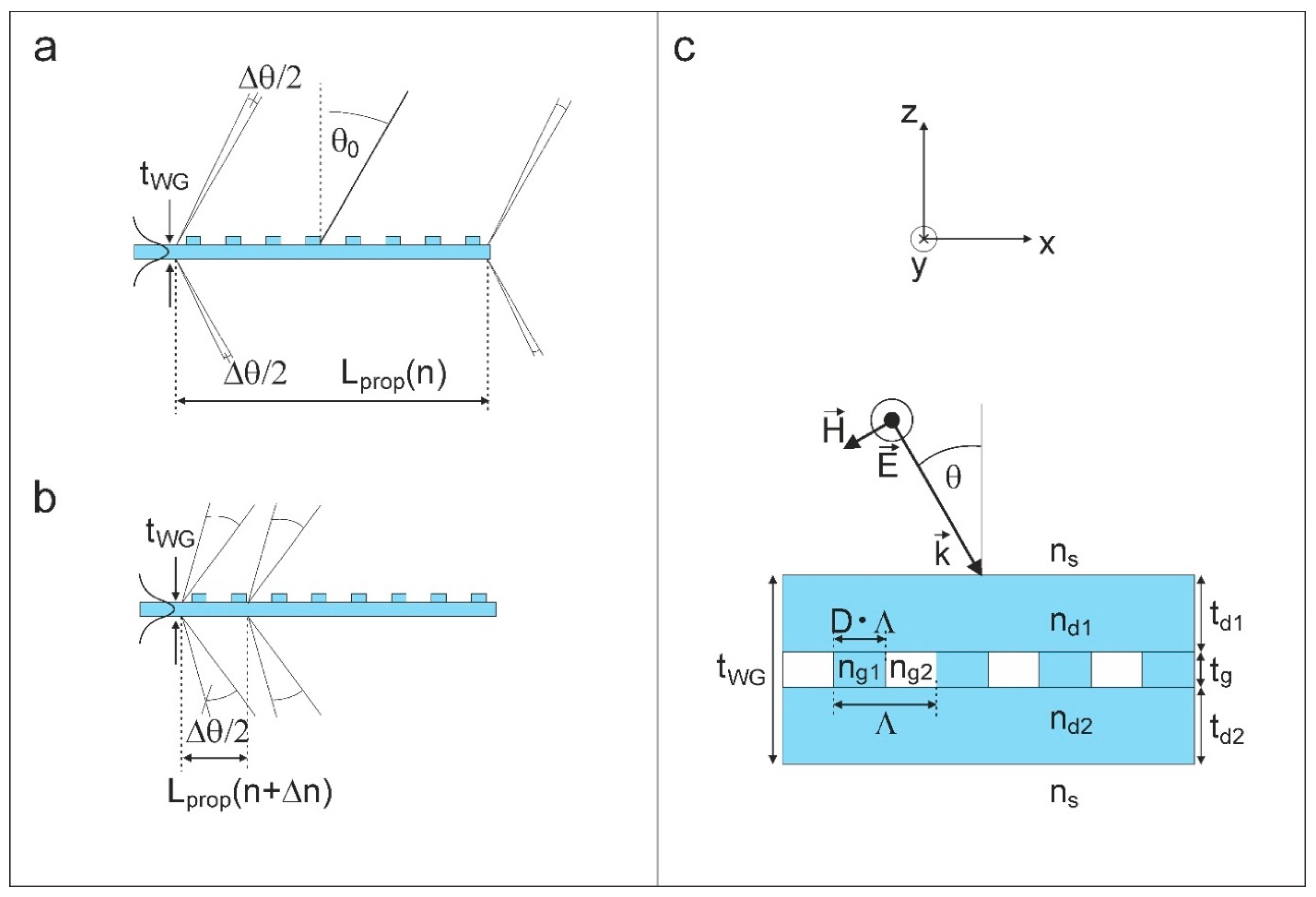
2.1. Definition of Geometry and Symmetry Parameters
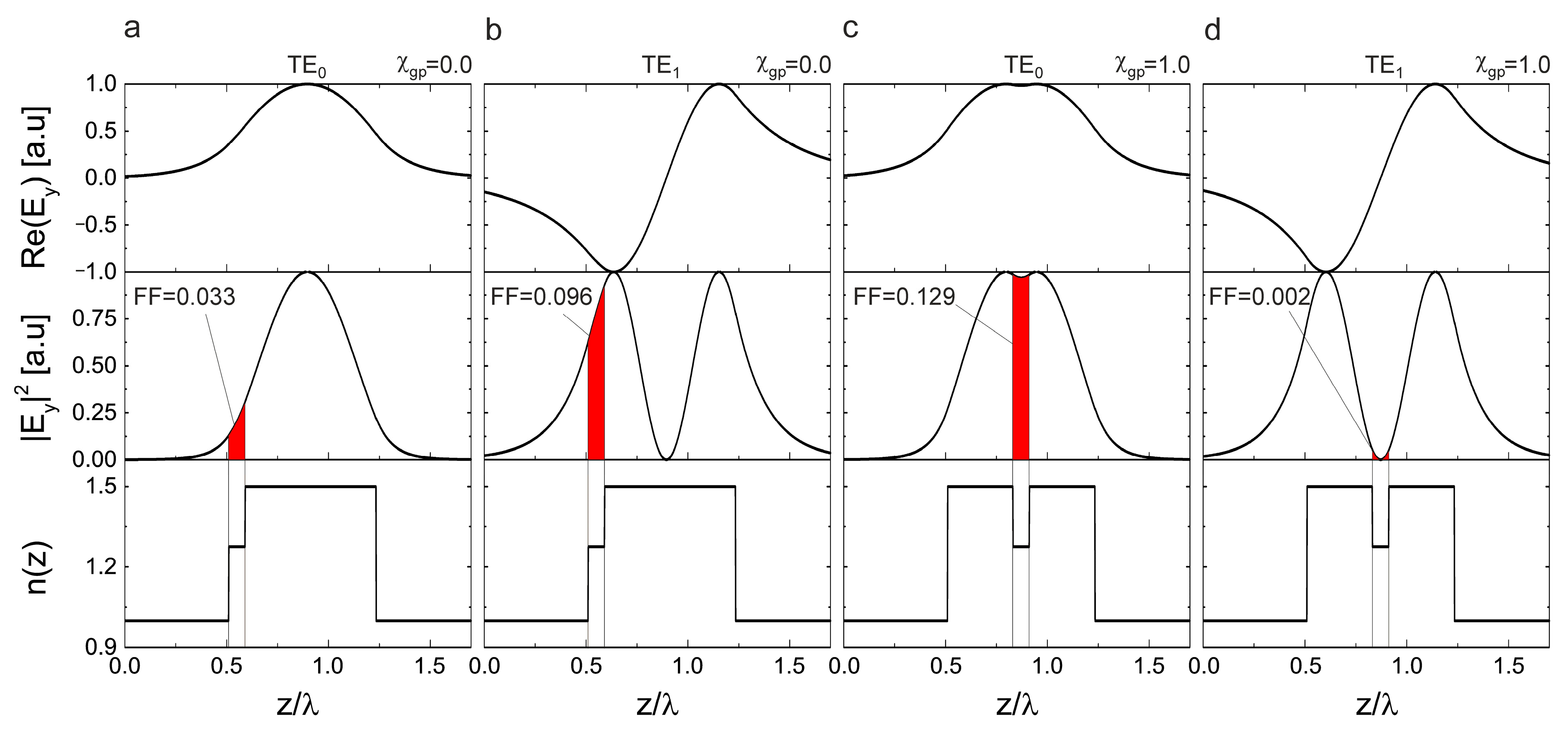
A visualization of the sensitivity of the propagation length with respect to refractive index changes is shown in Figure 1a,b. Light propagates through a waveguide grating mode in the positive x-direction. Due to the interaction with the grating, light is emitted into free space with a propagation length under a mean angle and with an angular divergence of . Without a change in the refractive index, the propagation length is large, and is small. When a refractive index change is introduced, the propagation length is much shorter, and is larger. Detailed equations on these relations are provided later in this text.
Figure 1.
(a) A waveguide grating with an eigenmode of large propagation length and, thus, a small angular divergence . is the mean angle under which light is emitted; (b) a shorter propagation length and larger under refractive index tuning ( ); (c) the definition of the geometry parameters of the proposed waveguide grating. TE-polarized light is considered. Further details are provided in the text.
To present a strategy for how a large sensitivity of the propagation length can be achieved, we used the geometry of a waveguide grating, which is defined by the parameters in Figure 1c. It consists of an infinitely extended rectangular grating of period Λ, refractive indices and , and a duty cycle . Two dielectric layers of thicknesses and , as well as refractive indices and , surround the grating. For all simulations in this research, we considered s-polarized plane-wave incidence (TE) in the x–z plane, with a lateral momentum .
To provide a measure of symmetry for both the waveguide grating’s refractive indices and thicknesses, we defined the symmetry parameters as
and
where “gp” represents the grating position, and “n” represents the refractive index profile. Values of and indicate a fully symmetric waveguide grating.
2.2. Geometry with
To introduce some measures of interest and explain the role of the mode, as well as the role of symmetry, we defined a waveguide grating with the parameters , , , (), and , and compared the cases of (Figure 2a,b) and (Figure 2c,d). As it is known from the literature, such a waveguide grating exhibits eigenmodes () that can be found for distinct real-valued lateral momenta , whereby is the effective refractive index of an eigenmode. The index counts the number of nodes of the electric field distribution attributed to an eigenmode. Thus, the has no nodes of , while the mode exhibits exactly one node of . This node causes an interesting behavior of the filling factor of the grating layer
where and define the first and second interface of the grating layer with respect to . While relatively large values of between 0.033 and 0.129 occur for all asymmetric cases as well as for the mode at , we observe a substantially lower value of for the mode when .
Figure 2.
The distributions of the normalized electric field and normalized intensity as well as filling factors () of two exemplary waveguide grating geometries with , , , () and : (a) TE0 mode at ; (b) TE1 mode at ; (c) TE1 mode at ; (d) TE1 mode at .
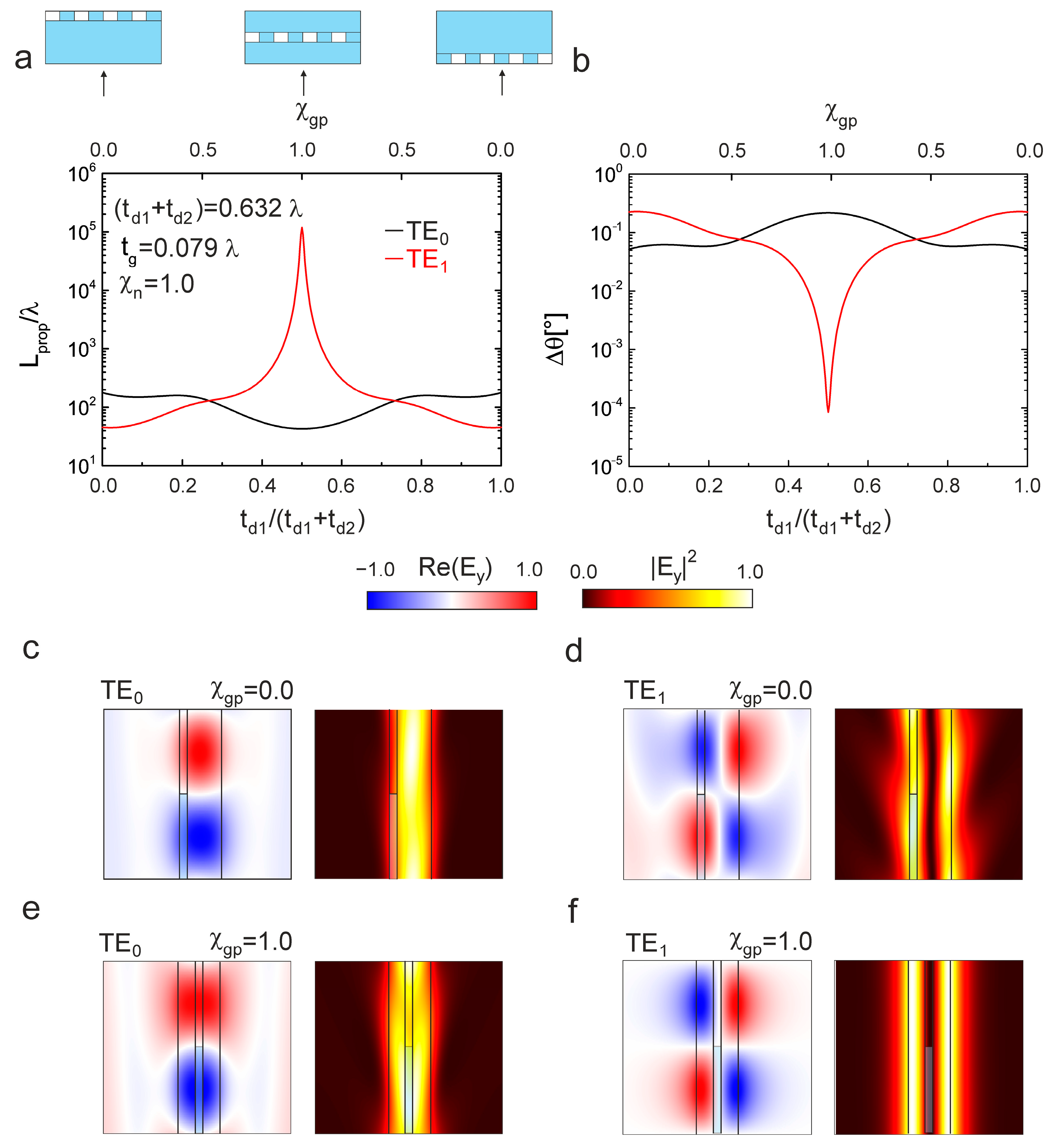
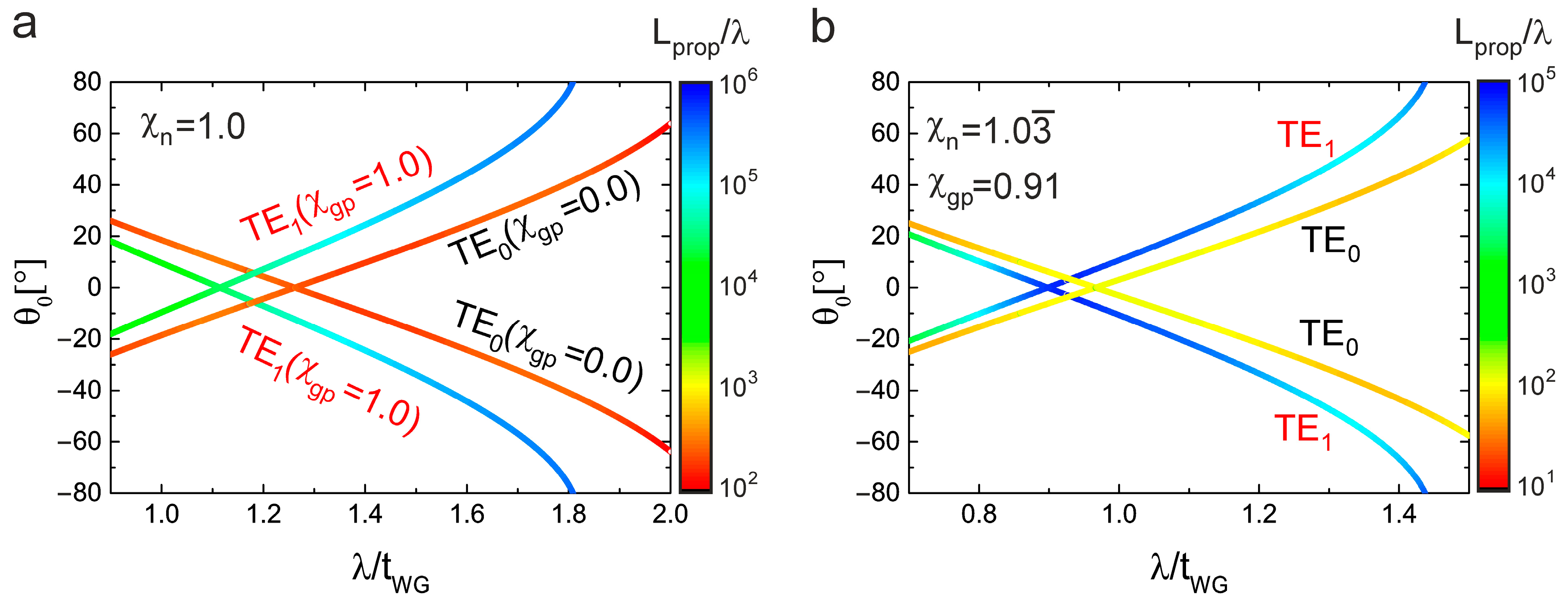
2.3. Geometry with with Variation in Symmetry Parameters
The grating () acts as a discrete lateral momentum reservoir providing a set of lateral momenta as a result of Floquet’s theorem [28]. The physical consequence of this set of momenta is that a mode of initial lateral momentum couples to free-space modes for . As a result, the initially real-valued becomes complex-valued. The intensity of an excited mode dampens to 1/e of its initial value by radiation over the normalized propagation length due to radiation into free-space modes. Radiated light enters the free space under an angle of and angular divergence of the diffracted light of . Here, we chose , , with otherwise identical parameters as for the waveguide grating discussed in Figure 2. Figure 3a,b show and as functions of with fixed values of , and (the grating position is shifted through a waveguide grating of fixed thickness). For , we obtained small values of of around and large values of of around , for both the and the mode. Strikingly, for , the mode exhibits large values of and small values of the divergence angle around . The distributions of and in Figure 3c–e for the and mode at , as well as for the mode at , are spatially distorted in comparison to the corresponding ones in Figure 2. Such distortions can be understood as radiation sources and indicate that the grating strongly couples guided waves to radiating waves. For the mode at (Figure 3f), almost no such distortion can be observed.
Figure 3.
Variation in the asymmetry parameter of a waveguide grating with , and under a constant value of . All other parameters are identical to the ones discussed in Figure 2: (a) the normalized propagation length and (b) the divergence angle of the mode (black) and mode (red); (c–f) normalized electric fields and intensities of the mode and mode for and .
This behavior of , , and the field distributions originates from the small value of discussed in Figure 2: empirically, for thin gratings (), we find the relation
We observed that the mode at exhibits , and thus, . In comparison, the mode at and as well as the mode at show . These dependencies presumably occur because the radiative loss rate of the grating scales with and the filling factor approximately scales with and , respectively. As a side note, gratings with dominant Ohmic losses (e.g., metallic gratings) show scalings of ( mode, ) and for all other cases.
Figure 4a,b show and with variation in at a fixed value of . Decreasing values of lead to increasing values of and decreasing values of with the explained proportionalities. These trends can be observed up to a value of , corresponding to .
Figure 4.
(a) The normalized propagation length and (b) the divergence angle of the mode (black) and mode (red) with variation in the normalized grating thickness for (dashed lines) and (solid lines) and a fixed normalized waveguide grating thickness ; (c,d) corresponding plots with variation in the normalized waveguide grating thickness and a fixed normalized grating thickness .
Figure 4c,d show and with variation in at a fixed value of . is strongly increased for the mode at in comparison to all other displayed cases for all values of above the cutoff of the mode.
Thus, as long as is small, compared with , and is large enough to support the mode, its increased values of and decreased values of can be obtained over a broad range of waveguide grating thicknesses in the case of and .
To present an impression of the meaning of these values in an optical application, we considered the mode and for a wavelength of nm with a grating thickness of nm. For these values, we obtained . In comparison, the standard scenario of a mode and leads to µm. To reach the same as for the mode at , the grating thickness would have to be reduced to 0.88 nm (a factor of 1/56) or the waveguide grating thickness (for nm) would have to be increased to approximately 7 µm (a factor of 15). Therefore, for a given grating geometry and waveguide grating thickness, using the mode at allows for a drastic increase in the propagation length in comparison to standard waveguide gratings using the mode.
Figure 5a shows the dispersion relation of the mode at and the mode at , with fixed ratios of all other geometry parameters (identical values to the ones in Figure 3 and Figure 4). Remarkably, large values of between and are observed for the mode over a broad spectral range between and . This behavior occurs due to the symmetry of the waveguide grating, which enforces the node of the mode to remain at the center plane of the waveguide grating. Therefore, regardless of the wavelength, an equivalent situation as discussed in Figure 3 is apparent when is below the cutoff of the mode.
Figure 5.
(a) The dispersion relations and normalized propagation lengths of the TE0 mode for and the TE1 mode for under fixed ratios of all geometry parameters as used in Figure 3 (only the wavelength is varied with respect to the geometry) and ; (b) dispersion relations and normalized propagation lengths for an asymmetric geometry with , for both the mode and mode with .
In comparison, the mode exhibits values of between and for all values of .
For an asymmetric geometry (), shows a maximum of around at a distinct value of (Figure 5b) for the mode. This maximum occurs since the position of the node of shifts through the waveguide grating with respect to the z-direction as a function of , and the largest value of is observed when is minimized.
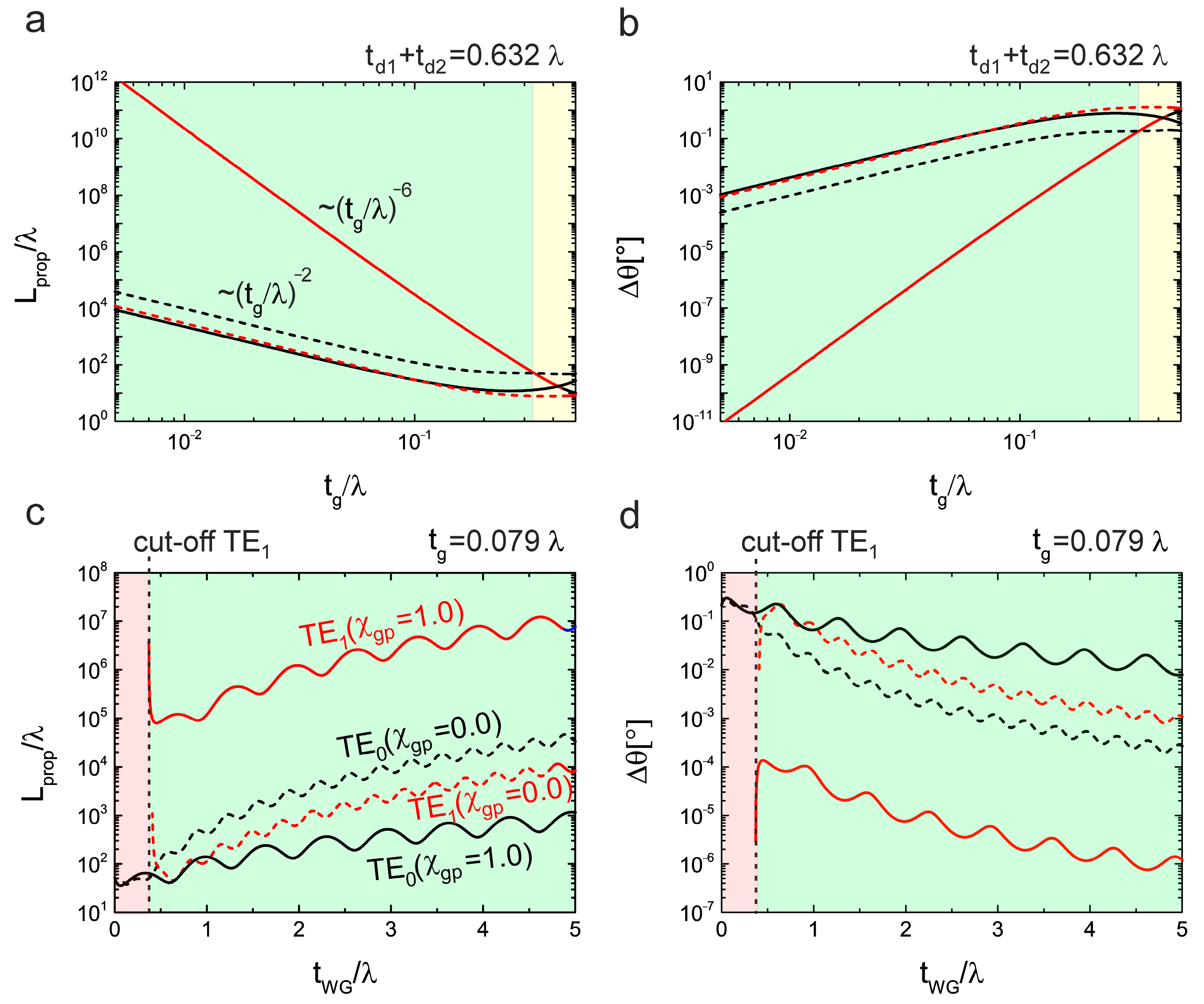
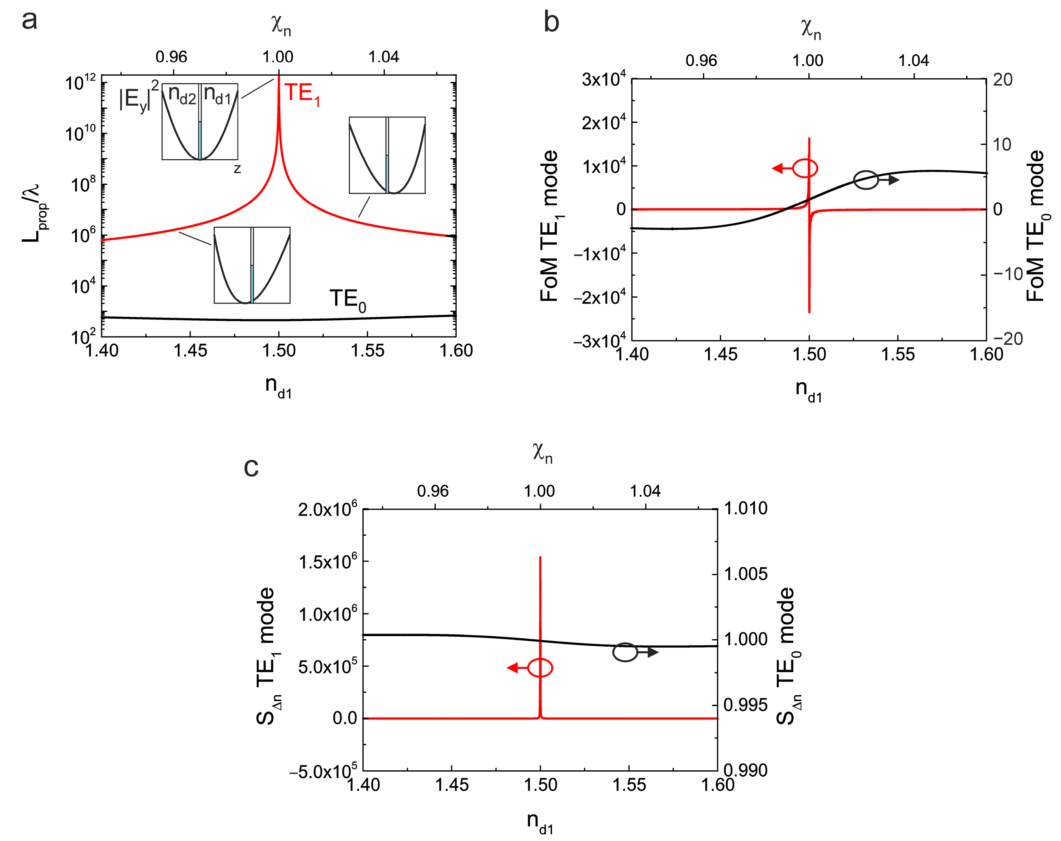
2.4. Sensitivity to Asymmetric Refractive Index Changes
In the last part of this study, we analyze the sensitivity of the waveguide grating with respect to an asymmetric change in the refractive index at . Such an asymmetric change in the refractive index means that is varied, and remains fixed at a value of . As a side note, variations in both and at show almost no sensitivity for the mode for any symmetric geometry, as is always minimized.
For this exemplary case, the grating thickness was chosen to be , whereby all other remaining geometry parameters were chosen to be the same as in Figure 3 and Figure 4.
The following two simulation observations are of interest in order to investigate the sensitivity of the waveguide grating:
(1) For small changes of the refractive index, the figure of merit
provides a measure for the sensitivity.
(2) For more practical considerations, the refractive index is commonly switched between two distinct values, with a difference of . The sensitivity can be defined by
Figure 6 shows both and the corresponding , as well as as a function of for the mode and the mode. Similar to the variation in in Figure 3, Figure 4 and Figure 5, the mode exhibits high values of around of when approaches 1.0. Most strikingly, strongly varies with changing values of (Figure 6a). In comparison, the mode exhibits nearly constant values of around . The of the mode reaches values of up to , whereas the maximum of the mode in the displayed range is (Figure 6b). The reason for this large for the lies in a strong decrease in consequent to symmetry breaking. Concerning (Figure 6c), for a value of (e.g., in the Pockels effect [18,19]), the values of are close to 1 for the mode.
However, for the mode, it can be observed that exhibits a maximum at , with a substantially higher value of around , in comparison to the mode. Although fully bound modes () cannot be reached, as the filling factor cannot be set to zero, the mode allows obtaining much higher propagation lengths and sensitivities with respect to asymmetric refractive index changes than the mode using the same geometry. In comparison, reports in the literature regarding the sensitivity of the propagation length with respect to refractive index sensitivity are around and for [21,22].
3. Conclusions
The results presented in this study show a way to drastically increase both the propagation length and sensitivity of waveguide grating by using the mode, as long as the grating thickness is small, compared with the waveguide grating thickness. As all results were obtained with the help of an exemplary set of waveguide grating geometries, further optimizations for specific applications such as different refractive indices and grating shapes should be considered in future studies. Nonetheless, as the increased propagation length and sensitivity result from symmetrical conditions, the concept at hand can be applied to a broad range of geometry parameters and wavelengths in general. Control over the propagation length cannot be provided only by changing the refractive index but also by breaking the geometric symmetry of the waveguide grating, e.g., by thermomechanical effects. To be sure, this property also implies the necessity of the accurate control of thickness homogeneity. From the practical point of view, symmetric and homogeneous waveguide gratings can be approached by lamination [29] and are, therefore, in principle, accessible with precise standard fabrication techniques such as roll-to-roll coating [30] in combination with lithography methods [31,32]. Thus, we anticipate this concept to be suited for large-area applications requiring control of the propagation length and divergence angle over many orders of magnitude or sensitivity to environmental changes. Obvious applications are spatially resolved refractive index sensors and light modulators.
4. Methods
All simulations in this research were conducted using rigorous coupled-wave analysis (RCWA) [28]. To ensure the stability of the simulation, we checked both the convergence of the simulated values as well as the conservation of energy (see the Supporting Information). Naturally, as the presented data were calculated for TE polarization, fast convergence and large stability were already obtained for a low number of Fourier orders.
Supplementary Materials
The following supporting information can be downloaded at: https://www.mdpi.com/article/10.3390/opt3010008/s1, Figures S1: (a,b) The convergence of as a function of the number of Fourier orders at the smallest () and thickest grating layer thicknesses ; (c) energy conservation for various grating thicknesses at 15 Fourier orders. For all values, the energy is conserved, confirming the stability of the simulation. Figure S2: (a,b) and as a function of for a waveguide grating with a blaze grating geometry and otherwise identical parameters as in Figure 3. The black and red dots indicate the and modes for , respectively. Figure S3: (a,b) and as functions of for a waveguide grating with a lossy grating ( and ) and otherwise identical parameters as in Figure 3. The black and red lines indicate the and modes for , respectively. Figure S4: (a,b) and as a function of for a waveguide grating with otherwise identical parameters to the geometry in Figure 3 for .
Author Contributions
The manuscript was written through the contributions of all authors. Conceptualization, M.M. and P.G.; methodology, M.M. and P.G.; software, M.M.; validation, M.M., P.G., A.H. and M.B.; formal analysis, M.M. and P.G.; investigation, M.M. and P.G.; resources, P.G.; data curation, M.M.; writing—original draft preparation, M.M. and P.G.; writing—review and editing, M.M., A.H., M.B. and P.G.; visualization, M.M.; supervision, P.G.; project administration, P.G.; funding acquisition, P.G. All authors have read and agreed to the published version of the manuscript.
Funding
This research was funded by the European Research Council (ERC), grant number 637367 and the Federal Ministry of Education and Research, contract number 13N15390.
Institutional Review Board Statement
Not applicable.
Informed Consent Statement
Not applicable.
Data Availability Statement
The data in this study are available on request from the corresponding author. Supporting data are available in the Supporting Information.
Acknowledgments
For financial support, this project received funding from the European Research Council (ERC) under the European Union’s Horizon 2020 research and innovation program (Grant Agreement No. 637367), as well as the Federal Ministry of Education and Research (Photonics Research Germany funding program, Contract No. 13N15390).
Conflicts of Interest
The authors declare no conflict of interest.
References
- Belt, M.; Davenport, M.L.; Bowers, J.E.; Blumenthal, D.J. Ultra-low-loss Ta2O5-core/SiO2-clad planar waveguides on Si substrates. Optica 2017, 4, 532–536. [Google Scholar] [CrossRef]
- Yeniay, A.; Gao, R.; Takayama, K.; Gao, R.; Garito, A.F. Ultra-low-loss polymer waveguides. J. Light. Technol. 2004, 22, 154–158. [Google Scholar] [CrossRef]
- Rickman, A.; Reed, G.T.; Weiss, B.L.; Namavar, F. Low-loss planar optical waveguides fabricated in SIMOX material. IEEE Photonics Technol. Lett. 1992, 4, 633–635. [Google Scholar] [CrossRef]
- Yang, L.; Saavedra, S.S.; Armstrong, N.R.; Hayes, J. Fabrication and Characterization of Low-Loss, Sol-Gel Planar Waveguides. Anal. Chem. 1994, 66, 1254–1263. [Google Scholar] [CrossRef]
- Ura, S.; Inoue, J.; Kintaka, K.; Awatsuji, Y. Proposal of small-aperture guided-mode resonance filter. In Proceedings of the 2011 13th International Conference on Transparent Optical Networks, Stockholm, Sweden, 26–30 June 2011; pp. 1–4. [Google Scholar]
- Wang, S.S.; Magnusson, R. Design of waveguide-grating filters with symmetrical line shapes and low sidebands. Opt. Lett. 1994, 19, 919–921. [Google Scholar] [CrossRef]
- Kintaka, K.; Majima, T.; Inoue, J.; Hatanaka, K.; Nishii, J.; Ura, S. Cavity-resonator-integrated guided-mode resonance filter for aperture miniaturization. Opt. Express 2012, 20, 1444–1449. [Google Scholar] [CrossRef]
- Thurman, S.T.; Morris, G.M. Controlling the spectral response in guided-mode resonance filter design. Appl. Opt. 2003, 42, 3225–3233. [Google Scholar] [CrossRef]
- Wang, S.S.; Magnusson, R. Multilayer waveguide-grating filters. Appl. Opt. 1995, 34, 2414–2420. [Google Scholar] [CrossRef]
- Flanders, D.C.; Kogelnik, H.; Schmidt, R.V.; Shank, C.V. Grating filters for thin-film optical waveguides. Appl. Phys. Lett. 1974, 24, 194–196. [Google Scholar] [CrossRef]
- Kehl, F.; Follonier, S. Self-referenced waveguide grating sensor. Opt. Lett. 2016, 41, 1447–1450. [Google Scholar] [CrossRef]
- Song, F.; Xiao, J.; Xie, A.J.; Seo, S.-W. A polymer waveguide grating sensor integrated with a thin-film photodetector. J. Opt. 2013, 16, 15503. [Google Scholar] [CrossRef] [PubMed][Green Version]
- Zaytseva, N.; Miller, W.; Goral, V.; Hepburn, J.; Fang, Y. Microfluidic resonant waveguide grating biosensor system for whole cell sensing. Appl. Phys. Lett. 2011, 98, 163703. [Google Scholar] [CrossRef]
- Ferrie, A.M.; Wu, Q.; Fang, Y. Resonant waveguide grating imager for live cell sensing. Appl. Phys. Lett. 2010, 97, 223704. [Google Scholar] [CrossRef] [PubMed]
- Nellen, P.M.; Tiefenthaler, K.; Lukosz, W. Integrated optical input grating couplers as biochemical sensors. Sens. Actuators 1988, 15, 285–295. [Google Scholar] [CrossRef]
- Clerc, D.; Lukosz, W. Integrated optical output grating coupler as biochemical sensor. Sens. Actuators B Chem. 1994, 19, 581–586. [Google Scholar] [CrossRef]
- Vörös, J.; Ramsden, J.J.; Csúcs, G.; Szendrő, I.; De Paul, S.M.; Textor, M.; Spencer, N.D. Optical grating coupler biosensors. Biomaterials 2002, 23, 3699–3710. [Google Scholar] [CrossRef]
- Kumada, A.; Hidaka, K. Directly High-Voltage Measuring System Based on Pockels Effect. IEEE Trans. Power Deliv. 2013, 28, 1306–1313. [Google Scholar] [CrossRef]
- Gervais, F.; Fonseca, V. Lithium Tantalate (LiTaO3). In Handbook of Optical Constants of Solids; Academic Press: Cambridge, MA, USA, 1997; pp. 777–805. ISBN 978-0-12-544415-6. [Google Scholar]
- Weis, R.S.; Gaylord, T.K. Lithium niobate: Summary of physical properties and crystal structure. Appl. Phys. A 1985, 37, 191–203. [Google Scholar] [CrossRef]
- Wang, Q.; Zhang, D.; Huang, Y.; Ni, Z.; Chen, J.; Zhong, Y.; Zhuang, S. Type of tunable guided-mode resonance filter based on electro-optic characteristic of polymer-dispersed liquid crystal. Opt. Lett. 2010, 35, 1236–1238. [Google Scholar] [CrossRef]
- Forouzmand, A.; Mosallaei, H. Electro-optical Amplitude and Phase Modulators Based on Tunable Guided-Mode Resonance Effect. ACS Photonics 2019, 6, 2860–2869. [Google Scholar] [CrossRef]
- Görrn, P. Method for Concentrating Light and Light Concentrator. U.S. Patent 10,558,027, 2 July 2014. [Google Scholar]
- Rabe, T.; Görrn, P.; Lehnhardt, M.; Tilgner, M.; Riedl, T.; Kowalsky, W. Highly sensitive determination of the polaron-induced optical absorption of organic charge-transport materials. Phys. Rev. Lett. 2009, 102, 137401. [Google Scholar] [PubMed]
- Görrn, P.; Rabe, T.; Riedl, T.; Kowalsky, W. Loss reduction in fully contacted organic laser waveguides using TE 2 modes. Appl. Phys. Lett. 2007, 91, 041113. [Google Scholar]
- Ura, S.; Yamada, K.; Lee, K.J.; Kintaka, K.; Inoue, J.; Magnusson, R. Guided-mode resonances in two-story waveguides. In Proceedings of the 2017 19th International Conference on Transparent Optical Networks (ICTON), Girona, Spain, 2–6 July 2017; pp. 1–4. [Google Scholar]
- Görrn, P. Waveguide, Method of Projecting Light from a Waveguide, and Display. U.S. Patent 10,739,623, 20 October 2017. [Google Scholar]
- Tamir, T.; Zhang, S. Modal transmission-line theory of multilayered grating structures. J. Light. Technol. 1996, 14, 914–927. [Google Scholar] [CrossRef]
- Meudt, M.; Bogiadzi, C.; Wrobel, K.; Görrn, P. Hybrid Photonic–Plasmonic Bound States in Continuum for Enhanced Light Manipulation. Adv. Opt. Mater. 2020, 8, 2000898. [Google Scholar] [CrossRef]
- Park, J.; Shin, K.; Lee, C. Roll-to-Roll Coating Technology and Its Applications: A Review. Int. J. Precis. Eng. Manuf. 2016, 17, 537–550. [Google Scholar] [CrossRef]
- Guo, L.J. Nanoimprint Lithography: Methods and Material Requirements. Adv. Mater. 2007, 19, 495–513. [Google Scholar] [CrossRef]
- Lu, C.; Lipson, R.H. Interference lithography: A powerful tool for fabricating periodic structures. Laser Photon. Rev. 2010, 4, 568–580. [Google Scholar] [CrossRef]
Publisher’s Note: MDPI stays neutral with regard to jurisdictional claims in published maps and institutional affiliations. |
© 2022 by the authors. Licensee MDPI, Basel, Switzerland. This article is an open access article distributed under the terms and conditions of the Creative Commons Attribution (CC BY) license (https://creativecommons.org/licenses/by/4.0/).


