Abstract
Metamaterials, in the form of perfect absorbers, have recently received attention for sensing and light-harvesting applications. The fabrication of such metamaterials involves several process steps and can often lead to nonidealities, which limit the performance of the metamaterial. A novel reciprocal plasmonic metasurface geometry composed of two plasmonic metasurfaces separated by a dielectric spacer was developed and investigated here. This geometry avoids many common fabrication-induced nonidealities by design and is synthesized by a combination of two-photon polymerization and electron-beam-based metallization. Infrared reflection measurements revealed that the reciprocal plasmonic metasurface is very sensitive to ultra-thin, conformal dielectric coatings. This is shown here by using Al2O3 grown by atomic layer deposition. It was observed experimentally that incremental conformal coatings of amorphous Al2O3 result in a spectral red shift of the absorption band of the reciprocal plasmonic metasurface. The experimental observations were corroborated by finite element model calculations, which also demonstrated a strong sensitivity of the reciprocal plasmonic metasurface geometry to conformal dielectric coatings. These coatings therefore offer the possibility for post-fabrication tuning of the reciprocal plasmonic metasurface resonances, thus rendering this novel geometry as an ideal candidate for narrow-band absorbers, which allow for cost-effective fabrication and tuning.
1. Introduction
Optical metamaterials are a group of engineered materials that are composed of an arrangement of artificial structures, which result in properties that are not exhibited in naturally occurring compounds [1,2]. These unique optical properties can be used to produce extraordinary optical effects including giant optical activity [3,4], narrow band filters [5,6], perfect lensing [7,8], and perfect absorption [9,10], to name only a few of the most prominent, well-documented effects. In addition to enabling novel optical components and devices, the optical properties of metamaterials can be carefully tailored to the requirements of the application by changing the composition, geometry, and arrangement of the constituents [11].
Metamaterials with perfect absorption have attracted much attention as they allow the design of novel sensors for the detection of trace gasses [12,13,14,15], are used for increasing the efficiency of solar cells [16,17], and are also used as optical switches [18,19], for instance. In order to achieve perfect absorption, metamaterial designs that rely on heterostructures have shown promising results. These materials are composed of multiple, stratified constituents [9,10,13,14,15,20,21,22,23,24,25,26,27,28].
The fabrication of metamaterials requires complex nanofabrication techniques; for instance, colloidal lithography, nanosphere lithography, or focused ion beam writing are most frequently employed [25,26,27,28,29,30,31,32,33]. Due to the complexity of the fabrication processes, deviations from nominal geometries are often inevitable. One of the sources of such deviations that can result in a substantial degradation of the optical response of the heterostructure is the alignment of the metamaterial components. Thus, the identification of metamaterial geometries and fabrication approaches that eliminate these nonidealities are of critical importance.
In addition, toward the goal of realizing metamaterial designs that avoid crucial fabrication steps or simplify the fabrication process, metamaterials that allow the adjustment of the optical response by using simple, scalable sample size post-fabrication processes could lead to a substantial reduction in the fabrication time and materials. The central idea is that small adjustments in the optical response of the metamaterial may be accomplished without a change in the overall geometry of the metasurface. These small adjustments can instead be made by using a comparatively simple post-fabrication approach in which the metasurface is conformally coated with a dielectric [34].
We developed a reciprocal plasmonic metasurface geometry that simplifies the fabrication process of heterostructured metamaterials and thereby prevents nonidealities by avoiding the misalignment of the metasurface constituents by design [24]. Reciprocal plasmonic metasurfaces are composed of two plasmonic metasurfaces with reciprocal surface geometries that are separated by a dielectric spacer. We explored the optical response of reciprocal metasurfaces theoretically using finite element calculations and found that the geometry enables a post-fabrication adjustment of its spectral response by applying a thin conformal dielectric coating [24].
In this paper, we demonstrate for the first time that reciprocal plasmonic metasurfaces can be fabricated using two-photon polymerization techniques in combination with a simple metallization using electron-beam evaporation. The fabrication process, using only two main process steps, eliminates the requirement of crucial alignment steps between the top and bottom metasurface. We further explored the effect of subsequent ultra-thin conformal dielectric coatings on the spectral response of the reciprocal plasmonic metasurface. Our observations indicated that such dielectric coatings can induce a spectral red-shift of the main resonance of the reciprocal plasmonic metasurface, corroborating our previous theoretical findings.
2. Materials and Methods
A schematic of the unit cell of the investigated reciprocal plasmonic metasurface can be seen in Figure 1. The reciprocal plasmonic metasurface was composed of a rectangular Au bar array separated by a dielectric spacer from a rectangular hole array. A negative-tone photoresist polymer (IP-Dip), which is compatible with two-photon polymerization, was used as a dielectric spacer. Fused silica glass was employed as a substrate. The infrared optical response of the reciprocal plasmonic metasurface was calculated using finite element modeling (FEM) simulations through COMSOL. The calculations were performed for the wavelength range from 4 µm to 7 µm using periodic boundary conditions along a unit cell. Accurate dielectric function data for fused silica glass and IP-Dip were obtained using spectroscopic ellipsometry in the range from 2 µm to 33 µm and were used for the FEM calculations [33,35,36].
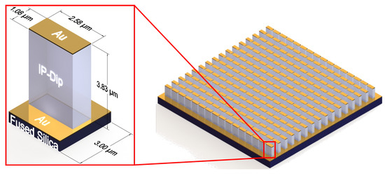
Figure 1.
Depiction of the square unit cell used in COMSOL modeling. The metasurface is composed of three layers: an IP-Dip polymer fin, a 50 nm Au dipole layer atop the fin, and a 50 nm layer surrounding the base of the fin. Fused silica is used as a substrate.
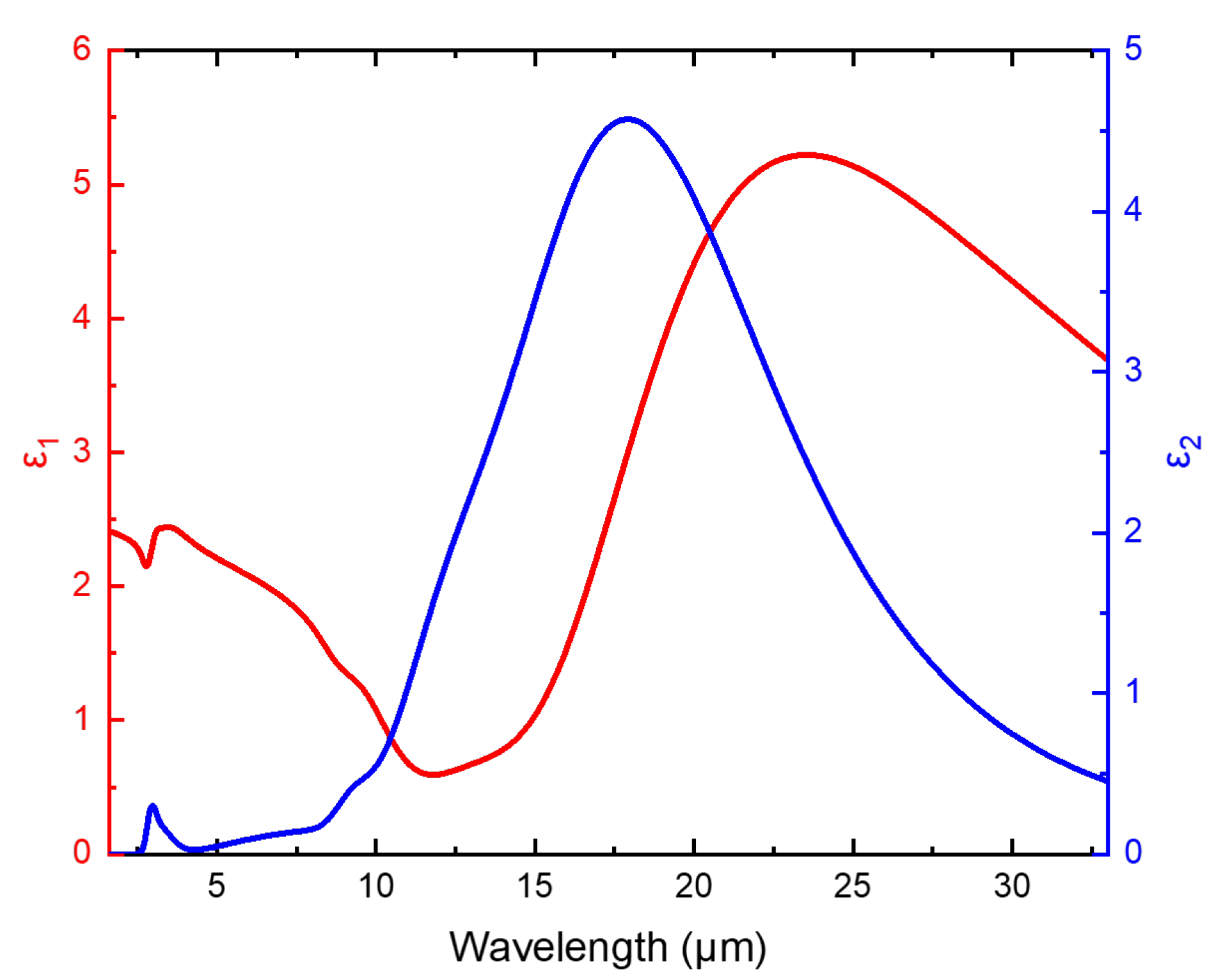
The effect of a conformal dielectric coating of amorphous Al2O3 on the spectral response of the reciprocal plasmonic metasurface was investigated for four different coating thicknesses: 10 nm, 20 nm, 30 nm, and 40 nm. A simple harmonic oscillator approach consisting of six Gaussian oscillators was used to describe the optical properties of the amorphous Al2O3 grown using atomic layer deposition. The real and imaginary parts of the model dielectric function ε1(λ) and ε2(λ), respectively, used for the COMSOL calculations can be seen in Figure 2. A summary of the parameterized Gaussian oscillators can be found in Table 1.
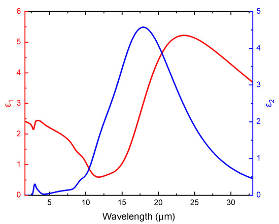
Figure 2.
Real ε1(λ) and imaginary ε2(λ) part of the model dielectric function of amorphous Al2O3 in the spectral range of 2 µm to 33 µm used for the COMSOL calculations reported here. The model dielectric function is composed of six Gaussian oscillators with the parameters summarized in Table 1.

Table 1.
Amplitude, center energy, and broadening parameters of the six Gaussian oscillators used to characterize amorphous Al2O3 in the wavelength range from 2 µm to 33 µm.
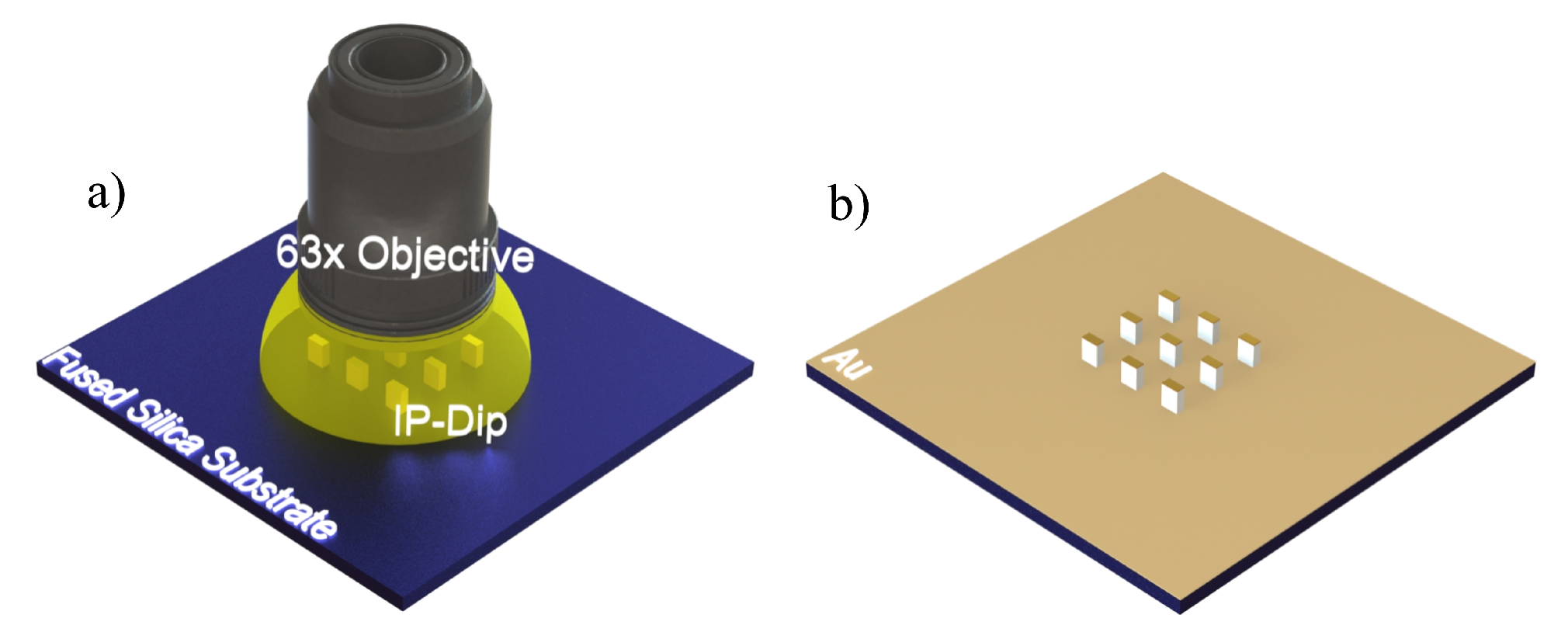
The reciprocal plasmonic metasurfaces investigated here were fabricated using a two-step process: two-photon polymerization followed by metallization, depicted in Figure 3.

Figure 3.
A schematic of the two-step fabrication method used to synthesize reciprocal plasmonic metasurfaces is shown. (a) Initially, rectangular fin arrays are additively manufactured using two-photon polymerization on a fused silica substrate. (b) Post-polymerization, the reciprocal metasurface sample is metalized using electron beam evaporation, simultaneously forming the top and bottom layers of the sample.
Prior to the two-photon polymerization step, the substrate was cleaned by rinsing with isopropanol-2, drying with N2, followed by a 5 min plasma cleaning using 12 SCCM flow of O2 at 13.56 MHz with a power of 150 W. The polymerization process was performed using a commercial two-photon lithography system (Photonic Professional GT, Nanoscribe GmbH), which employs a 780 nm femtosecond laser with an inverted microscope.
A 63× microscope objective was directly immersed into the monomer for the polymerization of a rectangular fin array, as shown in Figure 3. The laser beam position in the sample plane was controlled through a galvanometer. The position of the laser beam normal to the sample plane was controlled via a piezo actuator. To ensure structure quality and promote adhesion of the polymer to the substrate, the exposure parameters were optimized by adjusting the laser power and write speed prior to the sample fabrication. After polymerization was completed, the excess monomer was removed by immersing the sample into propylene glycol monomethyl ether acetate followed by isopropanol-2 for five minutes each. Once the excess monomer had been removed, the sample was allowed to air dry at room temperature for approximately 5 min.
Subsequent to the direct laser writing of the fin structures, the sample was metalized using an electron beam deposition system (Kurt J. Lesker PVD 75). A 5 nm layer of Cr, sourced from Cr pieces (99.95%), and a 50 nm Au layer, evaporated from Au pellets (99.99%), were deposited at a rate of 1 Å/s and 3 Å/s, respectively. The metallization resulted in the formation of a reciprocal plasmonic metasurface (see Figure 1). A rectangular bar array was placed on the top of the dielectric fins and a rectangular hole array on the substrate surrounding the bottom of the dielectric fins. All depositions were conducted at room temperature at a pressure of 2.53 × 10⁻⁵ Pa. The substrate holder was rotated during the deposition at approximately 15 rotations per minute to ensure a homogeneous film thickness across the sample.
The metasurface was characterized using polarized infrared reflection measurements to determine its infrared optical response. Linearly polarized reflectance spectra were captured using a Hyperion 3000 microscope (Bruker) in combination with a Vertex 70 FTIR spectrometer (Bruker). The reflectance measurements were carried out in the spectral range 4 µm to 7 µm with a resolution of 0.05 µm. A 15× IR Schwarzschild objective and 20 µm × 20 µm aperture, resulting in an average angle of incidence of 8.7∘, was used in combination with a mercury cadmium telluride detector for all infrared reflection measurements. A wire-grid polarizer mounted in a rotation stage was used to polarize the incident radiation.
In order to experimentally explore the effect of ultra-thin conformal dielectric coatings on the spectral location of the reciprocal plasmonic metasurface resonance, Al2O3 coatings were deposited using atomic layer deposition (Cross flow Savannah G2) in 10 nm thickness increments up to 40 nm. The depositions were carried out at 80 ∘C using trimethylaluminum (TMA) as a precursor and H2O as an oxidizer. The chamber pressure was kept at 10.7 Pa. Alternating 0.015 s-long pulses of TMA and H2O were used to grow the Al2O3 film with a growth rate of 0.8 Å/cycle. The growth rate was determined using ex situ spectroscopic ellipsometry in the visible spectrum. Four subsequent depositions of 10 nm films were grown with one-hundred twenty-five cycles each. Infrared reflectance measurements were conducted between each iteration to characterize the spectral response of the metasurface. COMSOL-based FEM model calculations were carried out for the corresponding conformal coating thicknesses for the comparison with the experimental infrared reflectance data.
3. Results and Discussion
Figure 4 shows the experimental reflectance spectrum of the as-fabricated reciprocal plasmonic metasurface without any dielectric coating. The incident radiation was polarized along the long axis of the rectangular dipoles forming the top metasurface, as shown in Figure 1. The reflectance spectra were dominated by a reflection minimum with a center wavelength of 4.8 µm. This reflectance minimum was due to a resonant absorption caused by the reciprocal plasmonic metasurface at that wavelength. A second, much smaller reflection minimum, could be observed at 5.8 µm. This feature was due to an absorption band of IP-Dip, which was used as a dielectric spacer in the reciprocal plasmonic metasurface and can be easily recognized in the imaginary part of the dielectric function of the polymerized IP-Dip reported earlier [35].
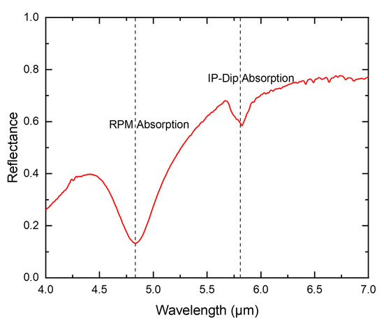
Figure 4.
Experimental reflectance spectrum of the fabricated reciprocal plasmonic metasurface without any dielectric coating. The experimental data were obtained at 8.7∘ incidence with a polarization parallel to the long axis of the rectangular fins. The resonance of the reciprocal plasmonic metasurface can be observed at 4.8 µm. The absorption feature, located at 5.8 µm, is due to an absorption band in the dielectric spacer (see Figure 1) [35].
The origin of the absorption in reciprocal plasmonic metasurfaces was investigated theoretically using FEM and analytical effective-medium-based calculations in [24]. These calculations indicated that a constructive interference within the dielectric spacer can be formed due to the coupling between the top and bottom metasurfaces. The FEM calculations further indicated that the field enhancement between the dielectric spacer fins resulted in the extreme sensitivity of the optical response to minute and local ambient index changes [24].
It can be noted that the overall amplitude of the experimental reflection spectrum presented in Figure 4 was lower than what was reported in [24] obtained from FEM calculations assuming an ideal reciprocal metasurface geometry. We tentatively attributed this deviation in the reflection amplitude to imperfections in the reciprocal metasurface geometry.
The metasurface was coated by subsequent conformal layers of Al2O3 at 10 nm per iteration to monitor the effect of these thin dielectric coatings on the reciprocal plasmonic metasurface resonance. The thickness of each subsequent dielectric coating was monitored using a witness sample, which was characterized by ex situ spectroscopic ellipsometry. The reflectance measurements were performed between each deposition starting at a coating thickness of 10 nm. The radiation was incident to the sample plane at 8.7∘ and polarized along the long axis of the top dipole layer.
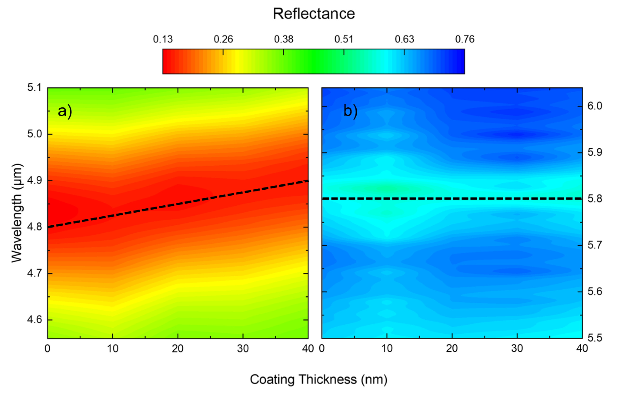
Figure 5 shows the experimental reflectance as a function of wavelength and coating thickness in the spectral vicinity of the reciprocal plasmonic metasurface resonance (a) and the IP-Dip absorption band (b) for comparison. Figure 5a clearly shows that the reflectance minimum associated with the reciprocal plasmonic metasurface resonance followed a linear spectral shift from λ = 4.8 µm for the uncoated sample to λ = 4.9 µm for a coating thickness of 40 nm. In comparison, the IP-Dip absorption band depicted in Figure 5b did not shift as a function of the Al2O3 coating thickness. This was as expected, because this is an intrinsic property of polymerized IP-Dip.
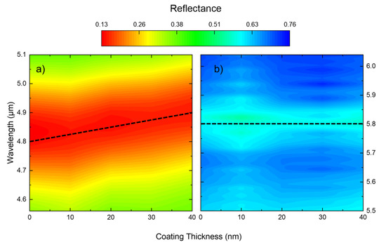
Figure 5.
False-color map of the reflectance of the reciprocal plasmonic metasurface as a function of the coating thickness and wavelength centered on the plasmonic metasurface resonance (a) and the IP-Dip absorption band (b), respectively. Whereas a shift of the center absorption wavelength as a function of dielectric coating thickness can be easily observed in (a), the IP-Dip absorption band shown in (b) is not affected, as expected.
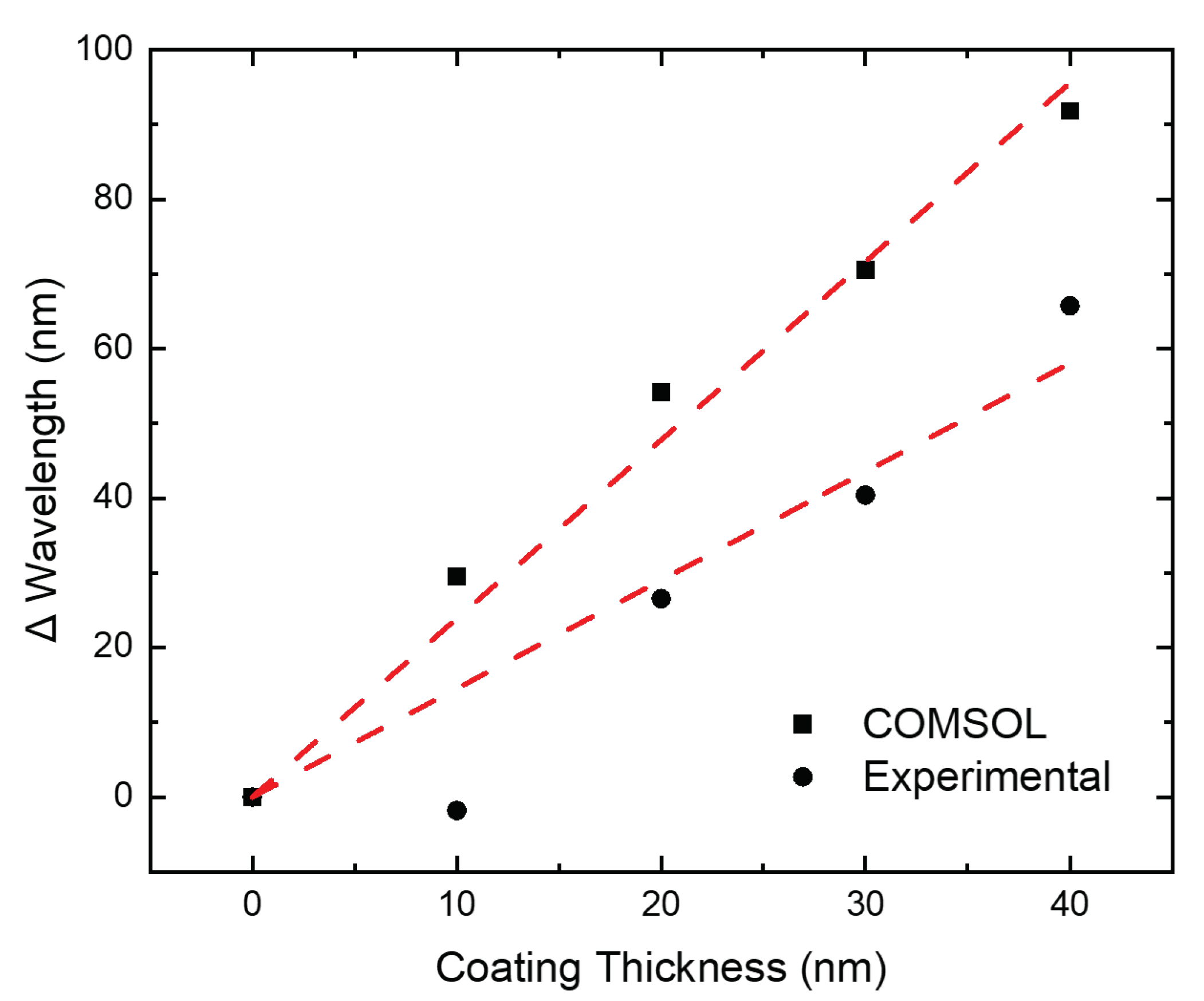
Figure 6 illustrates the experimentally observed wavelength shift of the reciprocal plasmonic metasurface resonance in comparison to the FEM-based model calculations (COMSOL). A linear trend can be recognized in the experimental data, as well as in the numerical simulations. We determined the slope of the wavelength shift for the experimental data to be 1.5, which is only sightly smaller than the slope of 2.4 for the data obtained using the numerical calculations. It can be further noticed that while the numerical calculations increased monotonically, the first experimental data point obtained for a thickness of 10 nm was virtually identical to the one obtained for the uncoated reference measurement. We tentatively attributed this behavior to the non-conformal coating of the reciprocal plasmonic metasurface. This could be caused by the high aspect ratio of the dielectric spacer fins, approximately 3:2 and 7:2 for the long and short axes, respectively. Initial growth delay was observed for atomic layer deposition on planar surfaces; however, the impact of the surface topology on the growth rate is not well known.
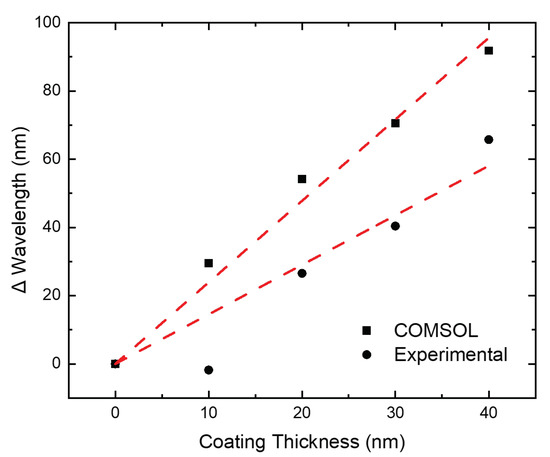
Figure 6.
Experimental results delineating the effects of incremental conformal coatings of amorphous Al2O3 deposited on reciprocal plasmonic metasurfaces. The main absorption peak represented in Figure 4 at 4.8 µm red-shifts after 10 nm increments.
4. Conclusions
Reciprocal plasmonic metasurfaces were experimentally demonstrated and characterized for the first time. The samples were synthesized using a two-step fabrication process. In the first step, two-photon lithography was used to deposit dielectric spacer fins. During the second step, electron beam evaporation of Au was employed to metalize the top of the dielectric spacers and the substrate surface, thereby forming two plasmonic metasurfaces with reciprocal geometries. This two-step fabrication technique is advantageous, as it ensures the alignment of the reciprocal surfaces by design.
Experimental infrared reflection measurements revealed the expected reciprocal plasmonic metasurface resonance, which was observed for the investigated geometries at 4.8 µm. The location of this resonance was confirmed using finite element calculations. After incremental conformal coatings of the reciprocal plasmonic metasurface with Al2O3 using atomic layer deposition, a shifting of the resonance wavelength was observed. It was found that the wavelength shift depended linearly on the Al2O3 coating thickness. The reciprocal plasmonic metasurface geometry therefore offers the tunability of the absorption wavelength through a thin conformal coating of a dielectric.
To conclude, the reciprocal plasmonic metasurface provides a novel geometry for scalable and tunable metamaterials. The simple configuration and sensitivity to thin conformal dielectric films demonstrated the reciprocal plasmonic metasurface as an adaptable platform for the rapid prototyping. In addition, the conformal dielectric coatings were shown to enable the adjustment of the metasurface resonances.
Author Contributions
Conceptualization, Y.L. and T.H.; methodology, M.M.; software, M.M.; validation, G.D.B., T.H., S.P. and V.P.S.; formal analysis, Y.L.; investigation, M.M.; resources, T.H.; data curation, M.M.; writing—original draft preparation, M.M. and T.H.; writing—review and editing, M.M., S.P., V.P.S., N.S., G.D.B. and T.H.; visualization, M.M.; supervision, T.H. and G.D.B.; project administration, T.H.; funding acquisition, T.H. All authors have read and agreed to the published version of the manuscript.
Funding
This research was funded by the National Science Foundation (1624572) within the IUCRC Center for Metamaterials and by the NSF MRI 1828430, the Army Research Office (W911NF-14-1-0299), and the Department of Physics and Optical Science of the University of North Carolina at Charlotte.
Acknowledgments
We would like to acknowledge the valuable discussions with Susanne Lee within the NSF IUCRC for Metamaterials.
Conflicts of Interest
The authors declare no conflict of interest. The funders had no role in the design of the study; in the collection, analyses, or interpretation of the data; in the writing of the manuscript; nor in the decision to publish the results.
References
- Cai, W.; Shalaev, V.M. Optical Metamaterials, 1st ed.; Springer Science+Business Media, LLC: New York, NY, USA, 2010; pp. 1–10. [Google Scholar]
- Sarychev, A.K.; Shalaev, V.M. Electrodynamics of Metamaterials, 1st ed.; World Scientific Publishing Co. Pte. Ltd.: Singapore, 2007; pp. 1–18. [Google Scholar]
- Plum, E.; Fedotov, V.A.; Zheludevb, N.I. Optical activity in extrinsically chiral metamaterial. Appl. Phys. Lett. 2008, 93, 191911. [Google Scholar] [CrossRef]
- Decker, M.; Zhao, R.; Soukoulis, C.M.; Linden, S.; Wegener, M. Twisted split-ring-resonator photonic metamaterial with huge optical activity. Opt. Lett. 2010, 35, 1593–1595. [Google Scholar] [CrossRef] [PubMed] [Green Version]
- Stinson, V.P.; Park, S.; McLamb, M.; Boreman, G.; Hofmann, T. Photonic Crystals with a Defect Fabricated by Two-Photon Polymerization for the Infrared Spectral Range. Optics 2021, 2, 284–291. [Google Scholar] [CrossRef]
- Aly, A.H.; Elsayed, H.A.; Malek, C. Defect modes properties in one-dimensional photonic crystals employing a superconducting nanocomposite material. Opt. Appl. 2018, 48, 53–64. [Google Scholar] [CrossRef]
- Pendry, J.B.; Ramakrishna, S.A. Refining the perfect lens. Physica B 2003, 338, 329–332. [Google Scholar] [CrossRef]
- Tsang, M.; Psaltis, D. Magnifying perfect lens and superlens design by coordinate transformation. Phys. Rev. B 2008, 77, 035122. [Google Scholar] [CrossRef] [Green Version]
- Wu, D.; Liu, Y.; Li, R.; Chen, L.; Ma, R.; Liu, C.; Ye, H. Infrared perfect ultra-narrow band absorber as plasmonic sensor. Nanoscale Res. Lett. 2016, 11, 483. [Google Scholar] [CrossRef] [Green Version]
- Ghobadi, A.; Hajian, H.; Rashed, A.R.; Butun, B.; Ozbay, E. Tuning the metal filling fraction in metal-insulator-metal ultra-broadband perfect absorbers to maximize the absorption bandwidth. Photonics Res. 2018, 6, 168–176. [Google Scholar] [CrossRef]
- Liu, Y.; Zhan, X. Metamaterials: A new frontier of science and technology. Chem. Soc. Rev. 2011, 40, 2494–2507. [Google Scholar] [CrossRef]
- Liu, N.; Mesch, M.; Weiss, T.; Hentschel, M.; Giessen, H. Infrared Perfect Absorber and Its Application As Plasmonic Sensor. Nano Lett. 2010, 10, 2342–2348. [Google Scholar] [CrossRef]
- Ameling, R.; Langguth, L.; Hentschel, M.; Mesch, M.; Braun, P.V.; Giessen, H. Cavity-enhanced localized plasmon resonance sensing. Appl. Phys. Lett. 2010, 97, 253116. [Google Scholar] [CrossRef]
- Pohl, T.; Sterl, F.; Strofeldt, N.; Giessen, H. Optical Carbon Dioxide Detection in the Visible Down to the Single Digit ppm Range Using Plasmonic Perfect Absorbers. ACS Sens. 2020, 5, 2628–2635. [Google Scholar] [CrossRef] [PubMed]
- Shi, L.; Shang, J.; Liu, Z.; Li, Y.; Fu, G.; Liu, X.; Pan, P.; Luo, H.; Liu, G. Ultra-narrow multi-band polarization-insensitive plasmonic perfect absorber for sensing. Nanotechnology 2020, 31, 465501. [Google Scholar] [CrossRef] [PubMed]
- Mulla, B.; Sabah, C. Perfect metamaterial absorber design for solar cell applications. Wave Random Complex 2015, 25, 382–383. [Google Scholar] [CrossRef]
- Mann, S.A.; Garnett, E.C. Resonant Nanophotonic Spectrum Splitting for Ultrathin Multijunction Solar Cells. ACS Photonics 2015, 2, 816–821. [Google Scholar] [CrossRef] [PubMed]
- Zheludev, N.; Kivshar, Y. From metamaterials to metadevices. Nature Mater. 2012, 11, 917–924. [Google Scholar] [CrossRef] [PubMed]
- Qian, Z.; Kang, S.; Rajaram, V.; Cassella, C.; McGruer, N.E.; Rinaldi, M. Zero-power infrared digitizers based on plasmonically enhanced micromechanical photoswitches. Nat. Nanotechnol. 2017, 12, 969–973. [Google Scholar] [CrossRef]
- Song, Z.; Wang, K.; Li, J.; Liu, Q.-H. Broadband tunable terahertz absorber based on vanadium dioxide metamaterials. Opt. Express 2018, 27, 7148–7154. [Google Scholar] [CrossRef]
- Masyukov, M.; Grebenchukov, A.N.; Litvinov, E.A.; Baldycheva, A.; Vozianova, A.V.; Khodzitsky, M.K. Photo-tunable terahertz absorber based on intercalated few-layer graphene. J. Opt. 2020, 22, 095105. [Google Scholar] [CrossRef]
- Dao, T.D.; Doan, A.T.; Ngo, D.H.; Chen, K.; Ishii, S.; Tamanai, A.; Nagao, T. Selective thermal emitters with infrared plasmonic indium tin oxide working in the atmosphere. Opt. Mater. Express 2019, 9, 2534–2544. [Google Scholar] [CrossRef]
- Yao, Y.; Zhou, J.; Liu, Z.; Liu, X.; Fu, G.; Liu, G. Refractor materials and plasmonics based perfect absorbers. Nanotechnology 2021, 32, 132002. [Google Scholar] [CrossRef] [PubMed]
- Li, Y.; McLamb, M.; Park, S.; Childers, D.; Boreman, G.D.; Hofmann, T. Theoretical Study of Enhanced Plasmonic-Photonic Hybrid Cavity Modes in Reciprocal Plasmonic Metasurfaces. Plasmonics 2021, 16, 2241–2247. [Google Scholar] [CrossRef]
- Karl, P.; Mennle, S.; Ubl, M.; Flad, P.; Yang, J.-W.; Peng, T.-Y.; Lu, Y.-J.; Giessen, H. Niobium nitride plasmonic perfect absorbers for tunable infrared superconducting nanowire photodetection. Opt. Express 2021, 29, 17087–17096. [Google Scholar] [CrossRef] [PubMed]
- To, N.; Juodkazis, S.; Nishijima, Y. Detailed Experiment-Theory Comparison of Mid-Infrared Metasurface Perfect Absorbers. Micromachines 2020, 11, 409. [Google Scholar] [CrossRef] [Green Version]
- Bonin, G.O.; Barrow, S.J.; Connell, T.U.; Roberts, A.; Chesman, A.S.R.; Gómez, D.E. Self-Assembly of Plasmonic Near-Perfect Absorbers of Light: The Effect of Particle Size. J. Phys. Chem. Lett. 2020, 11, 8378–8385. [Google Scholar] [CrossRef]
- Hentchel, M.; Weiss, T.; Bagheri, S.; Giessen, H. Babinet to the Half: Coupling of Solid and Inverse Plasmonic Structures. Nano Lett. 2013, 13, 4428–4433. [Google Scholar] [CrossRef]
- Su, V.-C.; Chu, C.H.; Sun, G.; Tsai, D.P. Advances in optical metasurfaces: Fabrication and applications. Opt. Express 2018, 26, 13148–13182. [Google Scholar] [CrossRef]
- Genevet, P.; Capasso, F.; Aieta, F.; Khorasaninejad, M.; Devlin, R. Recent advances in planar optics: From plasmonic to dielectric metasurfaces. Opt. 2017, 4, 139–152. [Google Scholar] [CrossRef]
- Wang, W.; Ramezani, M.; Väkeväinen, A.I.; Törmä, P.; Rivas, J.G.; Odom, T.W. The rich photonic world of plasmonic nanoparticle arrays. Mater. Today 2018, 21, 303–314. [Google Scholar] [CrossRef]
- Dao, T.D.; Chen, K.; Ishii, S.; Ohi, A.; Nabatame, T.; Kitajima, M.; Nagao, T. Infrared Perfect Absorbers Fabricated by Colloidal Mask Etching of Al-Al2O3-Al Trilayers. ACS Photonics 2015, 2, 964–970. [Google Scholar] [CrossRef]
- McLamb, M.; Li, Y.; Stinson, P.; Hofmann, T. Metasurfaces for the infrared spectral range fabricated using two-photon polymerization. Thin Solid Films 2021, 721, 138548. [Google Scholar] [CrossRef]
- Franklin, D.; George, M.; Fraser, J.; Chanda, D. Atomic layer deposition tuning of subwavelength aluminum grating for angle-insensitive plasmonic color. ACS Appl. Nano Mater. 2018, 1, 5210–5216. [Google Scholar] [CrossRef]
- Fullager, D.B.; Boreman, G.D.; Hofmann, T. Infrared dielectric response of nanoscribe IP-dip and IP-L monomers after polymerization from 250 cm-1 to 6000 cm-1. Opt. Mater. Express 2021, 7, 888–894. [Google Scholar] [CrossRef]
- Li, Y.; Park, S.; McLamb, M.; Lata, M.; Schöche, S.; Childers, D.; Aggarwal, I.D.; Poutous, M.K.; Boreman, G.; Hofmann, T. UV to NIR optical properties of IP-Dip, IP-L, and IP-S after two-photon polymerization determined by spectroscopic ellipsometery. Opt. Mater. Express 2019, 9, 4318–4328. [Google Scholar] [CrossRef]
Publisher’s Note: MDPI stays neutral with regard to jurisdictional claims in published maps and institutional affiliations. |
© 2022 by the authors. Licensee MDPI, Basel, Switzerland. This article is an open access article distributed under the terms and conditions of the Creative Commons Attribution (CC BY) license (https://creativecommons.org/licenses/by/4.0/).


