Abstract
One of the nanoscale technologies that shows its capability of implementing integrated digital circuits with low power, high speed, and high density is quantum-dot cellular automata (QCA). The fundamental device for designing and implementing circuits in QCA is majority logic. In this paper, a novel energy-efficient QCA design of three-input AND/OR logic functions is proposed. This design can perform both AND and OR logic operations using the same structure with an achievement of 58% and 64% approximate reductions in power consumption compared to majority-based structures, and 31% and 32% approximate reductions in power consumption compared to the best available circuits, respectively. In addition, other physical constraints such as area and latency are improved and have better or similar results compared to the best existing circuits. The proposed circuit can be considered as a fundamental and better alternative to the majority gate for energy-efficient circuit design in QCA. This will pave the way for developing efficient large-scale QCA-based sequential and combinational circuits.
1. Introduction
The downscaling of the design and construction of integrated circuits in a complementary metal oxide semiconductor (CMOS) has faced difficult challenges due to its physical limitations [1]. Several studies have investigated and introduced different emerging nanotechnologies beyond the CMOS. Quantum-dot cellular automata (QCA) is one of the most competitive candidates of promising nanotechnologies that can overcome physical limitations such as energy efficiency, integration density, and switching frequency [2,3,4,5,6,7] compared to CMOS technology. In CMOS technology, the NAND, NOR, and NOT logic functions are the fundamental devices used to implement circuits. However, the basic logic devices used in QCA are majority gate and inverter. The property of the majority gate being the fundamental of QCA leads researchers to investigate new structures for the majority gate [8] and the optimum equivalent majority-based designs of different circuits such as arithmetic circuits [9,10,11,12,13,14,15,16,17], memory [18,19,20,21,22,23], reversible gate [24], comparator [25], etc. On the other hand, several researchers have proposed special QCA structures for particular functions such as multiplexer [26,27,28,29], XOR/XNOR [30], etc. The designs of these circuits were developed independently based on QCA cells’ position without relying on the fundamentals of QCA, i.e., majority gate.
As is known, logic AND, OR, and NOT are the basic realization units of Boolean functions in traditional Boolean logic design. These logic operators can be easily used for realizing any logic function following the well-known simplification methods, which result in one of two main standard representation forms, i.e., sum of products (SOP) and product of sums (POS). In QCA, AND and OR functions can be implemented using a three-input majority gate by fixing one of its inputs’ polarization to −1 and +1, respectively. These functions can perform AND and OR operations for two inputs per gate. Other designs of AND and OR functions were developed based on multiplexer designs [27]. These circuits are also limited to process up to two inputs per gate. Compared to majority-based circuits, two-input AND and OR functions are much easier to use for realizing and designing circuits in QCA due to the complexity of majority circuits. Even though different synthesis methodologies for majority logic networks have been proposed [31,32,33,34], it is not guaranteed that they result in optimized QCA designs in view of different constraints at the physical level such as area, latency, power, etc., due to their inputs’ and outputs’ limitation [35].
In this paper, energy-efficient QCA structures of three-input AND and OR functions are proposed. Unlike the existing AND and OR gates, which can perform operations for only two inputs, the proposed structures are developed to perform the operations for three inputs. To the best of the author’s knowledge, QCA circuits, developed to perform AND and OR functions specifically for three or more inputs without relying on the current two-input structures, are not available. The proposed circuits are also developed with an optimization priority given to energy dissipation based on relative positioning of QCA cells without considering the QCA structure of majority gate as a fundamental building unit. This results in three-input AND/OR structure with lower energy dissipation compared to its equivalent majority-based and existing circuits. This also leads to energy-efficient large-scale circuits, since the overall energy dissipation of any QCA circuit is determined by different factors, and one of the major factors is energy dissipation of the basic building unit used in the circuit [36]. In addition, other performance factors such as area and latency are enhanced due to the great minimization of gate and level counts.
2. Methodology
2.1. Proposed QCA Structures of a Three-Input AND/OR Function
AND and OR logic operations are the fundamentals for realizing simplified Boolean functions produced by the conventional reduction methods. As mentioned previously, AND and OR functions can be implemented in QCA using the basic unit, which is a three-input majority gate. However, the number of inputs that can be received in this gate is limited to two. The proposed low-power QCA structure can perform AND and OR operations for three inputs simultaneously. This structure is developed independently based on the relative positioning of QCA cells without using majority gate as a basic design unit. Designing logic structure with less number of cells, fewer inputs/outputs, and optimized clocking schemes, the energy dissipation will be minimized due to the improvement of energy changes during switching and state transitions. Therefore, the design is developed using 13 QCA cells in a single layer. The cells are placed in a square shape using eight QCA cells with the same clock zone and attached with three cells for inputs (), one cell for constant (−1/+1), and one cell for output (f). By setting the constant cell to logic 0, i.e., polarization of −1, the circuit will perform AND operation for the three inputs and deliver the output to f as shown in Figure 1a. For OR operation, the same structure is used except the constant cell, which is set to logic 1, i.e., polarization of +1 as shown in Figure 1b.
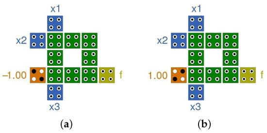
Figure 1.
QCA structures of proposed three-input AND/OR logic function: (a) three-input AND design; (b) three-input OR design.
From the figures, it can be noticed that both AND and OR functions can be obtained using the same design based on the value of the constant cell. This can be determined by
2.2. Development of n-Input AND/OR Logic Functions Based on the Proposed Structure
In QCA, gates and levels are two of the most significant factors that play a vital role in the overall circuit performance. This is due to the direct effect of these factors on different physical-level constraints such as area, latency, power consumption, etc. In addition, the number of basic logic devices used in a circuit mainly affects the reliability and probability of error [37,38] and the cost of the circuit [39]. Therefore, minimizing the number of gates and levels used in the circuit will improve the physical factors, and thus, the overall circuit performance will be enhanced. Unlike the majority-based AND and OR structures, which are limited to performing the operations for two inputs, the proposed structure can perform AND and OR operations for three inputs simultaneously using a single gate. This leads to reductions in the number of used gates and levels compared to the equivalent circuits developed based on majority gates. For instance, consider the three-input AND function and the three-input OR function . The QCA circuits of these functions can be designed using two cascaded majority-based gates of two-input AND and OR functions, i.e., and , respectively. However, by using the proposed structure, these functions can be implemented with a single gate. Figure 2 shows the block diagrams of these functions and the required number of gates and levels using majority and the proposed structure. From Figure 2a, it can be noticed that the majority-based design requires two cascaded gates in two levels, whereas one gate and one level are required using the proposed structure as shown in Figure 2b.
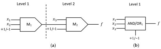
Figure 2.
Block diagram of three-input AND/OR logic function: (a) majority-based diagram; (b) proposed unit-based diagram.
Using the proposed structure for large-scale circuits with a large number of inputs, the required gates and levels can be reduced, which significantly enhances the circuit’s performance. By considering simplified Boolean functions expressed in one of two main standard representation forms that are sum of products (SOP) and product of sums (POS), terms in each of these forms are AND and OR logic operations of n inputs. The development of n-input AND/OR circuit using a majority-based gate or the proposed structure is based on a sequence of cascaded gates manner in which one gate at least in each level is required. This results in an equal number of gates used and the maximum number of levels in the designed circuit. Therefore, by reducing the number of gates, the number of levels will also be reduced. Figure 3a,b show the block diagrams of n-input AND/OR operation using majority gate and the proposed unit, respectively. From the diagrams, it can be noticed that in the majority-based circuit, only one input can be received to the operation at each level except the first level, where two inputs can be received. Thus, the number of gates (g) and maximum levels () using majority gates can be determined by
Using the proposed structure, three inputs in the first level and two inputs in each remaining level are allowed. This leads to fewer gates and levels required compared to majority-based designs. Therefore, the number of gates (g) and maximum levels () using the proposed three-input structure can be determined by
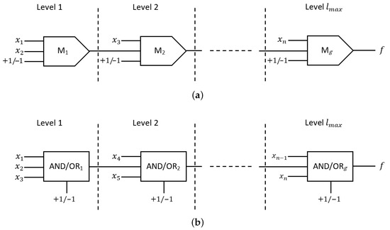
Figure 3.
Block diagram of n-input AND/OR logic function: (a) majority-based diagram; (b) proposed unit-based design.
For determining the maximum levels using majority-based or the proposed structures, it can be noticed that only one gate is placed in each level, and only single inputs are considered in each level, in addition to the output of the gate at the previous level. However, by placing more than one gate in each level and considering the combination of gate outputs as input to the gate in the next levels, the number of levels can be further reduced. For an n-input circuit developed using two-input AND/OR majority gates, the minimum number of levels is
For the proposed three-input AND/OR structure, the minimum number of levels can be determined by
Moreover, the proposed structure can be used to perform AND and OR operations for two inputs by fixing one of the inputs’ () polarization to +1 and −1, respectively. Among different choices of selecting one of the three inputs to be fixed, fixing the polarization of cell gives the optimum energy dissipation for both AND and OR circuits as shown in Figure 4.
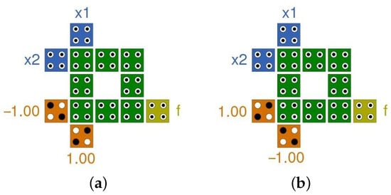
Figure 4.
QCA circuits of two-input AND/OR logic function based on the proposed structure: (a) two-input AND design; (b) two-input OR design.
3. Simulation Results and Comparison
In this section, the simulation results of the proposed structures and comparison with the existing circuits are presented. The proposed circuits are designed and simulated using QCADesignerE [36] (version 2.2) with the coherence vector engine. The coherence vector (w/energy) engine is also used for the calculation of power dissipation. The settings used for simulations and power calculations are given in Table 1.

Table 1.
Simulation settings used in QCA DesignerE.
Figure 5a,b show the simulation results of the proposed QCA structures of three-input AND and OR functions, respectively. From the figures, it can be seen that both circuits give correct and stable results.
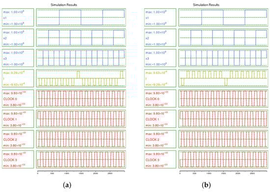
Figure 5.
Simulation results of the proposed three-input AND/OR circuits: (a) three-input AND circuit; (b) three-input OR circuit.
Comparison of power dissipation of the proposed three-input AND and OR structures and existing designs is given in Table 2. The table includes the energy dissipation for each input combination. The average of all these combinations is also calculated to give the average energy dissipation of the circuits. Other physical factors, i.e., area and latency, required for each circuit, are also given in the table. Since the existing QCA circuits of AND and OR operations are limited to two-input functions, the three-input circuits are designed by cascading two gates of their basic two-input structures to meet the functionality and to be comparable with the proposed structures. In this comparison, the circuits are also analyzed considering different clock zones as given in the table.
Table 2.
Comparison of the three-input AND/OR functions using the proposed and existing designs.
From the table, it can be noticed that the proposed structure of AND operation provides better energy dissipation, when using either one or two clock zones, with an approximate reduction of 55% and 58% compared to majority-based design in [36], and 26% and 31% compared to MUX-based design in [27], respectively. In addition, it produces better results in terms of area and latency compared to all best existing AND circuits. For OR operation, the proposed structure also provides better energy dissipation, when using either one or two clock zones, with an approximate reduction of 61% and 64% compared to majority-based design in [36], and 26% and 32% compared to MUX-based design in [27], respectively. It also has a smaller area and lower latency compared to the existing circuits.
Another comparison of power dissipation, area, and latency of AND and OR circuits for only two inputs using the proposed structures and existing circuits is given in Table 3.
Table 3.
Comparison of the two-input AND/OR functions using the proposed and existing designs.
The energy dissipation for each input combination and the average energy dissipation of the circuits are also given in the table. All three possible options for selecting the constant input for AND and OR functions are considered and compared. The circuit of each option is also compared when designing with different clock zones as given in the table.
From the table, it can be noticed that the proposed structures of both AND and OR operations have the optimum average energy dissipation when selecting as the constant and using one clock zone compared to the other constant selection options designed with one or two clock zones. These designs outperform the existing circuits except the circuit of AND function developed based on MUX design (1) in [27] and OR circuit developed based on MUX design (2) in [27]. However, the proposed designs obtained the optimum average energy dissipation with a latency reduction of 50% for both AND and OR circuits compared to the MUX-based designs in [27]. Even though the QCA structures in this paper are mainly proposed for energy-efficient three-input AND and OR functions, they also can be used to perform operations for two inputs with better results in terms of latency.
Figure 6 and Figure 7 show the number of gates, and minimum/maximum levels required using existing two-input and proposed three-input circuits, based on the number of function inputs, respectively. It can be seen that the proposed structures greatly contribute to the reduction of used gates and levels compared to the existing two-input AND/OR-based circuits. This leads to efficient circuits that outperform existing fundamental units in terms of energy dissipation and other physical factors such as area and latency.
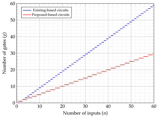
Figure 6.
Number of gates for existing- and proposed-based circuits.
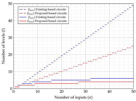
Figure 7.
Minimum/maximum levels for existing- and proposed-based circuits.
4. Conclusions
QCA is one of the promising technologies that can efficiently replace CMOS technology and overcome the challenges of physical limitations. In this paper, a novel QCA design of the fundamental AND and OR logic operations is proposed. Unlike existing circuits, which are limited to performing only two inputs, the proposed circuits can perform the operations for three inputs simultaneously. The design of these circuits is developed independently based on QCA cells’ positions without relying on the available basic building blocks such as majority gate. The proposed designs outperform the existing circuits in terms of energy dissipation. Moreover, they achieve better or similar results in other circuit parameters such as area and latency. These structures can be the basis for the development of a new synthesis methodology targeting efficient large-scale QCA-based sequential and combinational circuit design.
Funding
This research received no external funding.
Data Availability Statement
The original contributions presented in this study are included in the article. Further inquiries can be directed to the author.
Conflicts of Interest
The author declares no conflicts of interest.
References
- 2013 International Technology Roadmap for Semiconductors (ITRS). 2013. Available online: www.semiconductors.org (accessed on 28 March 2023).
- Lent, C.S.; Tougaw, P.D.; Porod, W.; Bernstein, G.H. Quantum cellular automata. Nanotechnology 1993, 4, 49. [Google Scholar] [CrossRef]
- Tougaw, P.D.; Lent, C.S. Logical devices implemented using quantum cellular automata. J. Appl. Phys. 1994, 75, 1818–1825. [Google Scholar] [CrossRef]
- Lent, C.S.; Tougaw, P.D. A device architecture for computing with quantum dots. Proc. IEEE 1997, 85, 541–557. [Google Scholar] [CrossRef]
- Porod, W. Quantum-dot devices and quantum-dot cellular automata. Intern. J. Bifurc. Chaos 1997, 7, 2199–2218. [Google Scholar] [CrossRef]
- Snider, G.; Orlov, A.; Amlani, I.; Zuo, X.; Bernstein, G.; Lent, C.; Merz, J.; Porod, W. Quantum-dot cellular automata: Review and recent experiments. J. Appl. Phys. 1999, 85, 4283–4285. [Google Scholar] [CrossRef]
- Walus, K.; Jullien, G.A.; Dimitrov, V.S. Computer arithmetic structures for quantum cellular automata. In Proceedings of the Conference Record of the Thirty-Seventh Asilomar Conference on Signals, Systems & Computers, Pacific Grove, CA, USA, 9–12 November 2003; Volume 2, pp. 1435–1439. [Google Scholar]
- Ahmadpour, S.; Jafari Navimipour, N.; Mosleh, M.; Noorallahzadeh, M.; Kassa, S.; Ahmed, S. A new fault-tolerance majority voter circuit for quantum-based nano-scale digital systems. J. Comput. Electron. 2025, 24, 149. [Google Scholar] [CrossRef]
- Safoev, N.; Jeon, J.C. Design and Evaluation of Cell Interaction Based Vedic Multiplier Using Quantum-Dot Cellular Automata. Electronics 2020, 9, 1036. [Google Scholar] [CrossRef]
- Babaie, S.; Sadoghifar, A.; Bahar, A.N. Design of an Efficient Multilayer Arithmetic Logic Unit in Quantum-Dot Cellular Automata (QCA). IEEE Trans. Circuits Syst. II 2019, 66, 963–967. [Google Scholar] [CrossRef]
- Bahar, A.N.; Wahid, K.A. Design of QCA-Serial Parallel Multiplier (QSPM) with Energy Dissipation Analysis. IEEE Trans. Circuits Syst. II 2020, 67, 1939–1943. [Google Scholar] [CrossRef]
- Abedi, D.; Jaberipur, G. Decimal Full Adders Specially Designed for Quantum-Dot Cellular Automata. IEEE Trans. Circuits Syst. II 2018, 65, 106–110. [Google Scholar] [CrossRef]
- Chu, Z.; Li, Z.; Xia, Y.; Wang, L.; Liu, W. BCD Adder Designs based on Three-Input XOR and Majority Gates. IEEE Trans. Circuits Syst. II 2020, 68, 1942–1946. [Google Scholar] [CrossRef]
- Sekar, K.; Marshal, R.; Lakshminarayanan, G. High-speed serial–parallel multiplier in quantum-dot cellular automata. IEEE Embed. Syst. Lett. 2021, 14, 31–34. [Google Scholar] [CrossRef]
- Alharbi, M.; Edwards, G.; Stocker, R. Reversible Quantum-Dot Cellular Automata-Based Arithmetic Logic Unit. Nanomaterials 2023, 13, 2445. [Google Scholar] [CrossRef]
- Yan, A.; Liu, R.; Cui, J.; Ni, T.; Girard, P.; Wen, X.; Zhang, J. Designs of BCD Adder Based on Excess-3 Code in Quantum-dot Cellular Automata. IEEE Trans. Circuits Syst. II Express Briefs 2023, 70, 2256–2260. [Google Scholar] [CrossRef]
- Chugh, H.; Singh, S. Efficient co-planar adder designs in quantum dot cellular automata: Energy and cost optimization with crossover elimination. Integration 2024, 94, 102103. [Google Scholar] [CrossRef]
- Song, Z.; Xie, G.; Cheng, X.; Wang, L.; Zhang, Y. An Ultra-Low Cost Multilayer RAM in Quantum-Dot Cellular Automata. IEEE Trans. Circuits Syst. II 2020, 67, 3397–3401. [Google Scholar] [CrossRef]
- Raj, M.; Gopalakrishnan, L.; Ko, S.B.; Naganathan, N.; Ramasubramanian, N. Configurable Logic Blocks and Memory Blocks for Beyond-CMOS FPGA-Based Embedded Systems. IEEE Embed. Syst. Lett. 2020, 12, 113–116. [Google Scholar] [CrossRef]
- Zhang, M.; Yang, X.; Cui, H.; Gu, Z.; Han, Z. A design methodology of line feedback shift registers with quantum cellular automata. IEEE Open J. Nanotechnol. 2021, 2, 129–139. [Google Scholar] [CrossRef]
- Jeon, J.; Almatrood, A.; Kim, H. Multi-Layered QCA Content-Addressable Memory Cell Using Low-Power Electronic Interaction for AI-Based Data Learning and Retrieval in Quantum Computing Environment. Sensors 2022, 23, 19. [Google Scholar] [CrossRef] [PubMed]
- Bhat, S.; Ahmed, S.; Bahar, A.; Wahid, K.; Otsuki, A.; Singh, P. Design of Cost-Efficient SRAM Cell in Quantum Dot Cellular Automata Technology. Electronics 2023, 12, 367. [Google Scholar] [CrossRef]
- Zhang, Y.; Zhu, C.; Cheng, X.; Xie, G. Design and Implementation of SRAM for LUT and CLB Using Clocking Mechanism in Quantum-Dot Cellular Automata. IEEE Trans. Circuits Syst. II Express Briefs 2022, 69, 3909–3913. [Google Scholar] [CrossRef]
- Seyedi, S.; Otsuki, A.; Navimipour, N.J. A New Cost-Efficient Design of a Reversible Gate Based on a Nano-Scale Quantum-Dot Cellular Automata Technology. Electronics 2021, 10, 1806. [Google Scholar] [CrossRef]
- Perri, S.; Spagnolo, F.; Frustaci, F.; Corsonello, P. Multibit Full Comparator Logic in Quantum-Dot Cellular Automata. IEEE Trans. Circuits Syst. II Express Briefs 2022, 69, 4508–4512. [Google Scholar] [CrossRef]
- Bahar, A.N.; Wahid, K.A. Design and Implementation of Approximate DCT Architecture in Quantum-Dot Cellular Automata. IEEE Trans. VLSI Syst. 2020, 28, 2530–2539. [Google Scholar] [CrossRef]
- Almatrood, A.; George, A.; Singh, H. Low-Power Multiplexer Structures Targeting Efficient QCA Nanotechnology Circuit Designs. Electronics 2021, 10, 1885. [Google Scholar] [CrossRef]
- Alharbi, M.; Edwards, G.; Stocker, R. An Ultra-Energy-Efficient Reversible Quantum-Dot Cellular Automata 8: 1 Multiplexer Circuit. Quantum Rep. 2024, 6, 41–57. [Google Scholar] [CrossRef]
- Sharma, V.; Kaushik, N. Ultra-optimized demultiplexer unit design in quantum-dot cellular automata nanotechnology. E-Prime-Adv. Electr. Eng. Electron. Energy 2024, 7, 100445. [Google Scholar] [CrossRef]
- Wang, L.; Xie, G. A Novel XOR/XNOR Structure for Modular Design of QCA Circuits. IEEE Trans. Circuits Syst. II 2020, 67, 3327–3331. [Google Scholar] [CrossRef]
- Zhang, R.; Gupta, P.; Jha, N. Majority and minority network synthesis with application to QCA-, SET-, and TPL-based nanotechnologies. IEEE Trans.-Comput.-Aided Des. Integr. Circuits Syst. 2007, 26, 1233–1245. [Google Scholar] [CrossRef]
- Kong, K.; Shang, Y.; Lu, R. An optimized majority logic synthesis methodology for quantum-dot cellular automata. IEEE Trans. Nanotechnol. 2009, 9, 170–183. [Google Scholar] [CrossRef]
- Wang, P.; Niamat, M.; Vemuru, S.; Alam, M.; Killian, T. Synthesis of majority/minority logic networks. IEEE Trans. Nanotechnol. 2015, 14, 473–483. [Google Scholar] [CrossRef]
- Ko, C.; Lin, C.; Chen, Y.; Wang, C. Majority logic circuit minimization using node addition and removal. IEEE Trans. Comput.-Aided Des. Integr. Circuits Syst. 2021, 41, 642–655. [Google Scholar] [CrossRef]
- Almatrood, A.; Singh, H. A comparative study of majority/minority logic circuit synthesis methods for post-CMOS nanotechnologies. Engineering 2017, 9, 890. [Google Scholar] [CrossRef][Green Version]
- Torres, F.S.; Wille, R.; Niemann, P.; Drechsler, R. An energy-aware model for the logic synthesis of quantum-dot cellular automata. IEEE Trans. Comput. Aided Des. Integr. Circuits Syst. 2018, 37, 3031–3041. [Google Scholar] [CrossRef]
- Krishnaswamy, S.; Viamontes, G.; Markov, I.; Hayes, J. Probabilistic transfer matrices in symbolic reliability analysis of logic circuits. ACM Trans. Des. Autom. Electron. Syst. (TODAES) 2008, 13, 1–35. [Google Scholar] [CrossRef]
- Han, J.; Chen, H.; Boykin, E.; Fortes, J. Reliability evaluation of logic circuits using probabilistic gate models. Microelectron. Reliab. 2011, 51, 468–476. [Google Scholar] [CrossRef]
- Liu, W.; Lu, L.; O’Neill, M.; Swartzlander, E. A first step toward cost functions for quantum-dot cellular automata designs. IEEE Trans. Nanotechnol. 2014, 13, 467–487. [Google Scholar] [CrossRef]
Disclaimer/Publisher’s Note: The statements, opinions and data contained in all publications are solely those of the individual author(s) and contributor(s) and not of MDPI and/or the editor(s). MDPI and/or the editor(s) disclaim responsibility for any injury to people or property resulting from any ideas, methods, instructions or products referred to in the content. |
© 2025 by the author. Licensee MDPI, Basel, Switzerland. This article is an open access article distributed under the terms and conditions of the Creative Commons Attribution (CC BY) license (https://creativecommons.org/licenses/by/4.0/).