Article

An Approach for Estimating the Reliability of IGBT Power Modules in Electrified Vehicle Traction Inverters

1
Centre for Hybrid Automotive Research and Green Energy (CHARGE) Labs, University of Windsor, Windsor, ON N9B 3P4, Canada
2
Corporate Engineering and R&D, Magna International Inc., Troy, MI 48098, USA
*
Author to whom correspondence should be addressed.
Vehicles 2020, 2(3), 413-423; https://doi.org/10.3390/vehicles2030022
Submission received: 1 June 2020 / Revised: 20 June 2020 / Accepted: 24 June 2020 / Published: 28 June 2020
(This article belongs to the Special Issue Future Powertrain Technologies)

Abstract

:
The reliability analysis of traction inverters is of great interest due to the use of new semi-conductor devices and inverter topologies in electric vehicles (EVs). Switching devices in the inverter are the most vulnerable component due to the electrical, thermal and mechanical stresses based on various driving conditions. Accurate stress analysis of power module is imperative for development of compact high-performance inverter designs with enhanced reliability. Therefore, this paper presents an inverter reliability estimation approach using an enhanced power loss model developed considering dynamic and transient influence of power semi-conductors. The temperature variation tracking has been improved by incorporating power module component parameters in an LPTN model of the inverter. A 100 kW EV grade traction inverter is used to validate the developed mathematical models towards estimating the inverter performance and subsequently, predicting the remaining useful lifetime of the inverter against two commonly used drive cycles.

1. Introduction

1.1. Background Literature of Inverter Reliability Estimation

Research shows that the power converter is the most vulnerable component in the electric vehicle (EV) powertrain since failure or maintenance of the converter is challenging due to inaccessibility [1]. Thus, research in the areas of inverter reliability estimation and condition monitoring towards design improvement, material optimization and control methods are vital for developing a high performance traction inverter. Towards inverter reliability estimation, developing an accurate model for analyzing temperature variation over a mission profile that affect the power module parameters is of prime importance [2,3,4,5]. Temperature variation due to random load profile causes thermal coefficient mismatch that leads to power module material degradation and subsequently towards critical failures like bond-wire lift off and solder fatigue in the power module. However, it is to be noted that the temperature variation within various components of the inverter depends on the load variation based on the mission profile.
In the literature, extensive research has been conducted to analyze and improve inverter reliability through improved control methodology, design parameter identification, and online and offline temperature tracking methods by considering specific mission profiles [5,6,7]. In order to perform reliability analysis on the inverter, accurate inverter loss model is important for device characterization, performance analysis and temperature estimation. The accuracy of the inverter loss model depends on the parasitic components in the circuit [8], which are difficult to determine experimentally. Hence, it is necessary to develop an accurate analytical model considering the effects of the parasitic components. The most fundamental inverter losses are the conduction and switching losses due to the current flow and switching speed during operation. In [9,10,11], inverter fundamental loss models have been developed with the device voltage and current characteristics. The energy dissipation map depending on the switching delay is used to determine switching loss of the inverter power switches. For further improvement, considering transient loss model improves the accuracy of inverter reliability estimation. In literature, the transient model has been developed to include turn -on voltage and resistance variation, parasitics components such as terminal capacitances and stray inductances [11]. However, all these influences have not been considered in the loss model towards reliability estimation. Hence, this paper aims at studying the influence of mission profile on reliability estimation considering the transient loss model. Mostly, transient model has been analyzed based on traditional double pulse test (DPT). The transient analysis is developed based on the behavior of parasitic capacitance on the terminals considering physical insights of the device, which increases the complexity of the analytical model. In [11], the parasitic influence considering terminal capacitances and stray induces have been developed based on the datasheet information and DPT test. However, it was challenging to consider temperature changes in the model with the conventional method. Therefore, this paper develops a transient model considering temperature in an iterative loop.
The inverter lifetime considering an EV powertrain has been estimated using power cycling test with a constant load or data driven load profile-based methods for maximum thermal stress analysis [12]. A constant heat generation model is developed to identify hotspot in the power module and bonding strength of the inverter [12,13,14,15,16]. Consequently, variable thermal cycling model is being to identify material degradation based on the average and maximum temperature swing. Finally, the reliability of the inverter estimated is directly related to the change in temperature due to the load variation in the mission profile. In a grid or EV powertrain, it is necessary to consider the data profile for actual lifespan analysis. Previous research on inverter lifetime analysis [17,18,19,20], considers the mission profile from the collected load curve based on consumers use. The conventional reliability analysis has been done with standard drive cycle which hardly match with practical scenario.

1.2. Contribution of This Paper

Considering the drawbacks of reliability estimation model in existing literature, this paper develops: (a) an advanced power loss model considering the dynamic and transient effect on the inverter 3-phase output voltage and current, (b) an extensive thermal network model based on inverter material properties to track temperature accurately during load variation and (c) detailed thermal cycle counting method for calculation of lifetime degradation incorporating bonding structure and solder layer dimension. Figure 1 shows the flowchart of the proposed inverter reliability estimation approach. In this paper, an improved inverter lifetime estimation model is developed incorporating an advanced power loss model with dynamic and transient effect such as device saturation, device parasitics on the 3-phase voltage and current for accurate thermal analysis. Cauer network based inverter thermal model is implemented to track temperature changes due to variation of power losses for any mission profile. Thermal network model considering device material information shows the temperature difference at each layer of the power module and accurate mean temperature due to consideration of transient effect in the power loss model. Also, the power loss model and thermal model are dependent on each other, which is updated in an iterative process. This improved power loss model is used to analyze the impact of mission profile for inverter reliability estimation. Finally, a Rainflow algorithm-based cycle counting algorithm is used to estimate remaining lifetime of the inverter. The main objective of this research is to develop an accurate reliability analysis and remaining useful lifetime estimation model of a traction inverter.

2. Electro—Thermal Model of 3-Phase VSI for Traction Application

The flowchart of the proposed lifetime estimation procedure is shown in Figure 1. First, the inverter power loss for every load condition is calculated. Following, the calculated power loss is used to observe corresponding temperature changes using the developed thermal network model. The extracted temperature is used as a feedback to the analytical loss model to improve accuracy. This paper considers a detailed inverter loss model considering saturation and non-linearity with parasitic components and an improved thermal network model for dynamic load conditions.

2.1. Improved Power Loss Model Considering Dynamic and Transient Effects

The inverter loss model is generalized for any power switching device. Also, it facilitates fast computation and considers variation of inverter parameters with the temperature changes. The developed model under dynamic operating conditions includes voltage saturation with changing load current, which elaborates conduction and switching losses [7]. Offline data from the device manufacturer has been used for initial condition. In this paper, the conduction loss of the Si-IGBT and Si-diode are modeled separately.
The overall conduction loss combines the losses from six switches. The conduction loss model depends on the current flowing through the device in the operation. Also, the collector—emitter terminal voltage shown in Figure 2a is considered. Both the diode and IGBT voltage and current characteristics have been fused together to simplify the calculation and limit the computational time. The graph also indicates the temperature dependency of the terminal voltage.
With the increase in temperature, the graph shifts in the upward direction. The voltage graph has been stored for room temperature and device maximum temperature. Additionally, linear interpolation method is applied to estimate voltage characteristics at any other temperature. Similarly, the conductive resistance is being calculated using the V–I characteristics with the varying temperature.
The energy dissipation during turn—on and off have been acquired with double-pulse test (DPT) method in Figure 3a. Related parameters of the diode and IGBT that have been used in loss and junction temperature calculations have been considered from the device datasheet in Table 1. A half bridge power module has been selected to conduct the DPT. The tests have been conducted at 400 V DC and settled temperatures of 25 °C and 125 °C. The related parameters such as threshold voltage and gate resistance have been stored at the two selected operating temperatures. The parameters in between the selected temperature range are determined by linear interpolation method. The external resistance has been considered based on the high switching operation, which is used to identify minimum switching loss. The initial parameters at the selected temperature have been obtained from the device datasheet and matched with the developed analytical model. Also, the parasitic elements are provided in Table 2. The change in parasitic elements are determined with respect temperature. Depending on the extracted parameters from the DPT, an extended switching loss model has been developed to determine energy dissipation during turn-on and turn-off of the power switches in dynamic operating condition. The switching loss model in (2), considers the on time and off time delay due to the internal and external gate resistance on the input terminal of the power switch. The internal gate resistance is modeled with respect to load current, applied gate voltage and temperature. In the off stage, diode loss is also added to the IGBT switch for simplification. Energy dissipation map during turn–on and off due to high switching operation is represented in Figure 2b. The power losses due to conduction and switching losses from (1) and (2) are considered for both the IGBT and diode with the non–ideality based on temperature variation and voltage saturation [9]. Where VCE0, Ic and RCE are the voltage, current and conductive resistance of a single IGBT device. Energy dissipation due to device switching is represented in (2), where ton and toff are the IGBT turn–on and off time and trr is the diode turn–off time. Vf represents the voltage due to terminal parasitics. The conduction loss is defined from the device V–I characteristics. In Figure 2c, the switching loss model considers the energy dissipation during turn–off and on through a look-up-table from the test inverter in Figure 3b. The fundamental parameters of the test inverter are given in Table 1, which is obtained from the device datasheet.
For transient analysis, effective parasitic components among power switch terminal collector, emitter and gate as in Figure 2c have been considered in (3) for accurate voltage measurement towards improved inverter loss model. To improve the accuracy of the inverter power loss model, a comprehensive transient response model has been developed [8,9]. The most significant effect in the transient stage is caused due to collector–gate and gate–emitter capacitance, which is also known as miller capacitance. The transient response of a switch depends on the capacitor charging and discharging factor. Therefore, it is important to monitor capacitor behavior in the switching period. The overall transient loss model is developed in (3)—(6). Threshold voltage is considered during sudden change in junction temperature. The parasitic capacitances are determined in rising and falling interval of the switching period. Previously, derived collector–emitter voltage is included in the model. Collector–emitter resistance, loop and leakage inductances in Table 2, are taken from the datasheet for room temperature, which is being updated in an iterative loop based on temperature.
P c o n d , Q ( T j , t ) = 1 2 V C E 0 ( T j ) π i ^ ( t ) + R C E ( T j ) 4 i ^ ( t ) 2 + M cos θ V C E 0 ( T j ) 8 i ^ ( t ) + R C E 0 ( T j ) 3 π i ^ ( t ) 2 P c o n d , D ( T j , t ) = 1 2 V f 0 ( T j ) π i ^ ( t ) + R f ( T j ) 4 i ^ 2 ( t ) + M cos θ V f 0 ( T j ) 8 i ^ ( t ) + R f ( T j ) 3 π i ^ 2 ( t )
E o n = 0 t o n V C E ( T j , t ) i c ( t ) d t E o f f = 0 t o f f + t r r V C E ( T j , t ) i c ( t ) d t P s w = 1 π f s [ E o n ( i ^ ) + E o f f ( i ^ ) ]
V f = g f s V t h + I C ( 1 + g f s R g ) C g C + C C E t
C g e = C i e s C r e s C c e = C o e s C r e s C g c = C r e s
i g = C g e d v g e d t + C g c d ( v g e v c e ) d t i c e = v c e R c e , o n + C c e d v c e d t C g e d ( v g e v c e ) d t
v g e = v c R g i g ( L g + L s ) d i g d t v c e = v d c v f L p d i c e d t
Rg and gfs represent gate resistance and trans-conductance of the semi-conductor. Gate resistance is stored as a look–up table. In (5) and (6), ig, ice, vge and vce represent the gate and collector to emitter current and voltage, respectively. Ls and Lg represent the leakage and gate inductances. CgC and Cce represent the parasitic capacitances between the terminal gate–collector and collector–emitter respectively.

2.2. Derivation of Electro—Thermal Model Parameters Considering Inverter Material Information

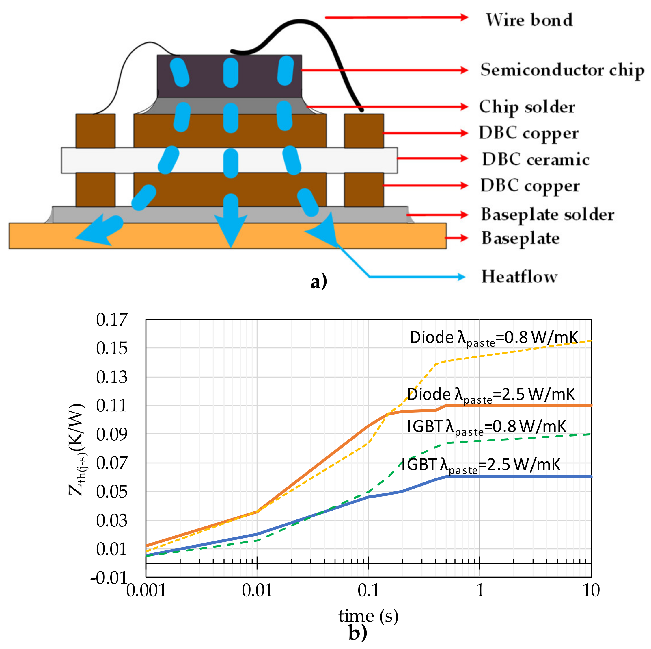
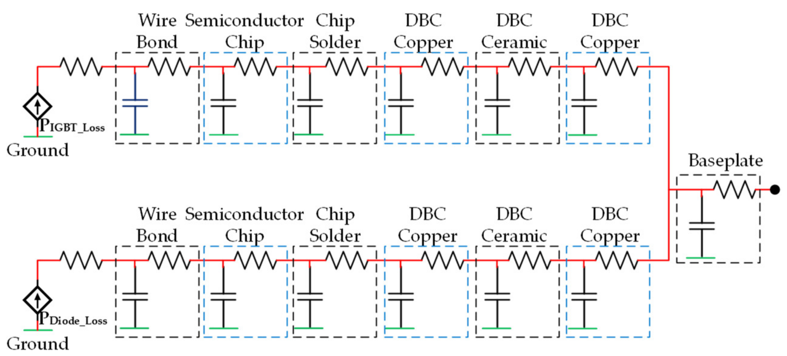
The reliability of the inverter is dependent on the thermal performance and heat distribution in the device module. The main reason for inverter failure is because of material degradation due to thermal co-efficient mismatch while the temperature changes. The thermal network model has been developed to analyze the thermal stress during load flow in the powertrain (Figure 4). The main objective of the thermal network model is to determine the average temperature and the temperature swing during operation. Further, the possibility of device failure such as solder fatigue and bond-wire lift off are dependent on average temperature and instant temperature variation. Thus, based on the packaging as in Figure 5, the thermal network model is developed for both IGBT and diode.
The most common thermal network model is based on Cauer type or Foster network type model. The Foster type model is based on the equivalent circuit model measured from a fitting function. The fitting function is developed from the transient thermal impedance analysis and updated with the linear estimation method. On the other hand, the Cauer type model is based on the material properties and the structure of the power module. The model parameter changes along with the change in material properties, which indicates the fault in the power module effectively. Therefore, this paper focuses on developing the Cauer type inverter thermal network to monitor the temperature changes at each layer of the power module. In this section, the nonuniform heat flow in the power module has been discussed. In the packaging power module heat flows from the top surface IGBT chip to the bottom surface heatsink. The center of the power module carries most of the temperature as the heat flows vertically. In the power module, chip is the most sensitive to heat condition. Also, the aging temperature Tj,side is mentioned in (7). The ∆Tj is to monitor the aging process and Tj,chip is the chip temperature at the center of the chip. d is the minimum distance:
Δ T j = T j , c h i p T j , s i d e d
In Figure 5, series combination of each thermal resistance and capacitance represent each layer of the device package in Figure 3b. The upper branch represents the heat flow path on the IGBT, and the lower branch shows the heat flow on the diode side. Also, the thermal co-efficient of the device material has been selected from the Table 1. The developed thermal network model represents heat flow at each layer of the device packaging module. The RC parameters are identified from the provided material information. The capacitor represents the dynamic temperature changes in dynamic condition. The capacitor represents the temperature rise with the time constant. The thermal model describes the temperature changes at each layer of the module package depending on the loss variation for random dynamic loading. The thermal network model has been developed based on the cross–sectional diagram in Figure 3b. The Zjc defines the sum of the all junction impedances at each layer of the power module. The total impedance combines the seven layers of the IGBT power module. The impedances at the first and the second layer from the top shows the self-heating path due to the die attached [12]. Also, the die in IGBT and diode cause cross heating due to the power loss of its own:
Z j c = k = 1 n R k 1 + s τ k
The Cauer-based RC thermal network model is expressed in (8). Zjc is the total impedance of the thermal model. k represents number of bond layers in the packaging device. If the power stops flowing into the power switches before it reaches the thermal equilibrium, the device will be steady at the ambient temperature due to the time constant, which depends on the thermal resistance and capacitance value. The time constant is calculated as in [13]. The temperature cooling curve can be represented as an exponential curve in (9):
T c a ( t ) = i = 1 n α i e ( t τ i )
The time constant is dependent on the RC parameters in (8). In (9), the time constant is converted into Laplace transfer function. Also, the model is developed for seven layers (n = 7) of the power module as in Figure 5:
T c a ( s ) = i = 1 n α i s + 1 τ i
The inverter thermal analysis is mostly described in 1-D model [12,13,14,15]. However, to improve accuracy in this paper third—order analytical model is used to track heat conduction in the power module from the chip to the heatsink. The final Cauer network model in Figure 3b, can be expressed with the Kirchhoff’s voltage law the third—order thermal model can be solved as in (11):
T c a ( t ) = α 1 e t τ 1 + α 2 e t τ 2 + α 3 e t τ 3

3. Reliability Performance of VSI under Different Mission Profile

After developing the electro-thermal model of the inverter, a comprehensive stress evaluation can be analyzed with specific load profile based on the inverter design specification for a time duration. This approach is called mission profile. To understand the influence of different mission profiles on reliability estimation, first, a temperature variation profile is estimated using the developed electro-thermal model. Further, using the Rainflow algorithm with extended cycle counting model, the number of temperature cycles is extracted.

3.1. Rainflow Algorithm-Based Inverter Reliability Estimation

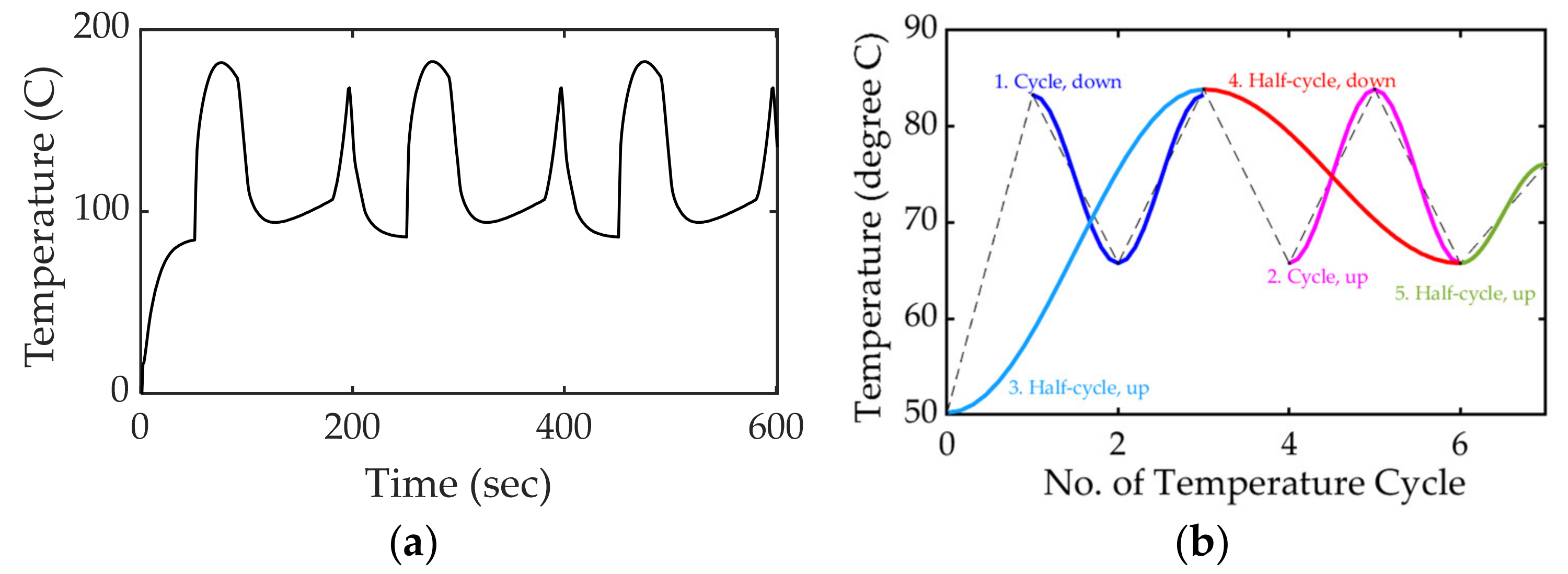
For a selected mission profile, the temperature variation of the device module estimated using the developed electro-thermal model is used as an input to the cycle counting algorithm. Subsequently, the offline algorithm is used to find the number of half cycles and full cycles along with their maxima and minima in the temperature profile. Figure 6 shows a sample cycle counting method for a short loading profile. A single 20 s profile has been repeated three times and it increases the temperature by 0.4 °C, which leads towards faulty condition. Figure 6a shows the dynamic performance of the thermal network model. Further, Figure 6b shows the number of half cycle and full cycle count for a single mission profile using the Rainflow algorithm, where a complete temperature swing is considered as a full cycle and each temperature rise or fall is considered as a half cycle [17]. A rising cycle is defined as cycle up and similarly falling half cycle is denoted as cycle down in Figure 6b. A comprehensive Arrhenius model in (12) is used to consider wire bond diameter and solder layer thickness to improve accuracy in reliability analysis. The material geometrical information such as the bonding wire thickness, layer area, height and solder joint material are taken from the manufacturer application note. In (12), Nf defines the number of cycles counted based on the mean temperature and maximum temperature swing in the selected mission profile. NDamage defines the accumulated damage due to the load variation in the mission profile and Ni and Nfi are the number of cycles for a specific temperature and the number of temperature cycles in the selected mission profile respectively. Finally, the inverter lifetime is calculated using the damage accumulation factor as in (12) where, K, β1β6 are the curve fitting co-efficient for cycle counting model. The fitting co-efficient are identified with linear curve fitting method. V, I and D represent the conducting voltage, current and the diameter of the wire bond.
N f = K ( Δ T j ) β 1 e β 2 T max t o n β 3 I β 4 V β 5 D β 6
N D a m a g e = N i N f i

3.2. Impact of Mission Profile on Inverter Remaining Useful Lifetime Estimation

The developed inverter lifetime estimation model has been implemented on an EV grade 100 kW inverter. The damage accumulation in the inverter due to load variation is estimated by the ratio of the initial lifecycle of the inverter and lifecycle after operating under a load profile in (13). The initial inverter state has been determined using device data information provided by the manufacturer. With the provided information ideal inverter condition has been determined and deviation due to load profile has been monitored to identify material degradation. Two most commonly used mission profiles namely Urban Dynamometer Driving Schedule (UDDS) and Worldwide Harmonized Light Vehicles Test Cycle (WLTC3) drive cycles as in Figure 7a,b have been selected for this analysis.
To reduce the computational time, cycles with major load changes have been considered for maximum temperature sweep. Also, mean temperature and maximum temperature swing based cycles have been considered to reflect the worst case loading conditions on the inverter. The cycle counting matrix obtained for UDDS and WLTC3 are shown in Figure 7c,d, respectively. First, the UDDS cycle is slightly longer in duration than the WLTC3 cycle. Also, the urban cycle has multiple small cycles, which shows the mean temperature variations in a small range of 354 K to 364 K. On the other hand, WLTC3 drive cycle consists of several low and high load conditions that lead to significant temperature variations. The mean temperature in WLTC3 in between 200 K to 450 K, shows a wide range of load variation, which implies additional stress on the inverter. Similarly, the UDDS has minimum temperature swing observed due to repetitive small cycles and the WLTC3 has maximum temperature swing. Finally, based on the mean temperature and temperature swing, the number of full cycles has been calculated. The number of cycles in UDDS is higher than WLTC3. However, the stress on the inverter is higher in the WLTC3 due to increased mean temperature and maximum temperature swing, which reduces the inverter lifetime by 1.03 years.

4. Conclusions and Future Work

In this paper, a concise inverter reliability prediction model has been developed with improved power loss and thermal models. The power loss model showed a significant effect of transient power loss, which leads to accurate temperature tracking. The thermal network model estimates the temperature difference at each layer of the power module to identify significant material degradation. Finally, the reliability estimation model showed the inverter damage over the selected standard driving range or mission profile. The inverter transient response model incorporating the parasitic elements improves the loss determination model. Also, it improves temperature tracking for random load changes in mission profile. Finally, from the analytical model, it can be concluded that the selected mission profiles have different load variation, which implies different stress level and causes difference in the estimation model by 1.03 years due to a greater number of load cycles in the WLTC3 mission profile, subsequently leading to reduced mileage over time. Hence, online reliability estimation model could be more accurate, which will avoid dependency on the data driven analysis in the conventional analysis. Also, inverter fault prognosis model will be incorporated in the future to observe increased temperature during fault period.

Author Contributions

Concept—A.K., K.L.V.I., N.C.K.; Methodology—A.K., K.L.V.I., N.C.K.; Analysis—A.K., A.B., P.K.; Resources—N.C.K., K.L.V.I.; Preparation Original Draft—A.K.; Writing, Reviewing and Editing—A.K., A.B., P.K., K.L.V.I. and N.C.K.; Supervision—N.C.K. and K.L.V.I. All authors have read and agreed to the published version of the manuscript.

Funding

This research is funded by Magna International, Ontario Center of Excellence (OCE), and Natural Sciences and Engineering Research Council of Canada (NSERC).

Conflicts of Interest

The authors declare no conflict of interest.

References

  1. Ni, Z.; Lyu, X.; Yadav, O.P.; Singh, B.N.; Zheng, S.; Cao, D. Overview of Real-Time Lifetime Prediction and Extension for SiC Power Converters. IEEE Trans. Power Electron. 2020, 35, 7765–7794. [Google Scholar] [CrossRef]
  2. Sangwongwanich, A.; Yang, Y.; Sera, D.; Blaabjerg, F. Mission Profile-Oriented Control for Reliability and Lifetime of Photovoltaic Inverters. IEEE Trans. Ind. Appl. 2018, 56, 2512–2518. [Google Scholar]
  3. Musallam, M.; Yin, C.; Bailey, C.; Johnson, M. Mission profile-based reliability design and real-time life consumption estimation in power electronics. IEEE Trans. Power Electron. 2015, 30, 2601–2613. [Google Scholar] [CrossRef] [Green Version]
  4. Sangwongwanich, A.; Yang, Y.; Sera, D.; Blaabjerg, F.; Zhou, D. On the Impacts of PV Array Sizing on the Inverter Reliability and Lifetime. IEEE Trans. Ind. Appl. 2018, 54, 3656–3667. [Google Scholar] [CrossRef] [Green Version]
  5. Ma, K.; Liserre, M.; Blaabjerg, F.; Kerekes, T. Thermal loading and lifetime estimation for power device considering mission profiles in wind power converter. IEEE Trans. Power Electron. 2015, 30, 590–602. [Google Scholar] [CrossRef]
  6. Wei, L.; McGuire, J.; Lukaszewski, R.A. Analysis of PWM frequency control to improve the lifetime of PWM inverter. IEEE Trans. Ind. Appl. 2011, 47, 922–929. [Google Scholar]
  7. Yang, K.; Guo, J.; Ge, H.; Bilgin, B.; Loukanov, V.; Emadi, A. Transient electro-thermal analysis for a MOSFET based Traction Inverter. In Proceedings of the 2014 IEEE Transportation Electrification Conference and Expo, Detroit, MI, USA, 15–18 June 2014; pp. 1–6. [Google Scholar]
  8. Li, X.; Jiang, J.; Huang, A.Q.; Guo, S.; Deng, X.; Zhang, B.; She, X. A SiC Power MOSFET Loss Model Suitable for High-Frequency Applications. IEEE Trans. Ind. Electron. 2017, 64, 8268–8276. [Google Scholar] [CrossRef]
  9. Xu, Y.; Ho, C.N.M.; Ghosh, A.; Muthumuni, D. A Datasheet-Based Behavioral Model of SiC MOSFET for Power Loss Prediction in Electromagnetic Transient Simulation. In Proceedings of the 2019 IEEE Applied Power Electronics Conference and Exposition (APEC), Anaheim, CA, USA, 17–21 March 2019; pp. 521–526. [Google Scholar]
  10. Roy, S.K.; Basu, K. Analytical Estimation of Turn on Switching Loss of SiC mosfet and Schottky Diode Pair From Datasheet Parameters. IEEE Trans. Power Electron. 2018, 34, 9118–9130. [Google Scholar] [CrossRef]
  11. Peng, H.; Chen, J.; Cheng, Z.; Kang, Y.; Wu, J.; Chu, X. Accuracy-Enhanced Miller Capacitor Modeling and Switching Performance Prediction for Efficient SiC Design in High-Frequency X-Ray High-Voltage Generators. IEEE J. Emerg. Sel. Top. Power Electron. 2020, 8, 179–194. [Google Scholar] [CrossRef]
  12. Ye, J.; Yang, K.; Ye, H.; Emadi, A. A Fast Electro-Thermal Model of Traction Inverters for Electrified Vehicles. IEEE Trans. Power Electron. 2017, 32, 3920–3934. [Google Scholar] [CrossRef]
  13. An, N.; Du, M.; Hu, Z.; Wei, K. A High-Precision Adaptive Thermal Network Model for Monitoring of Temperature Variations in Insulated Gate Bipolar Transistor (IGBT) Modules. Energies 2018, 11, 595. [Google Scholar] [CrossRef] [Green Version]
  14. Tsibizov, A.; Kovačević-Badstübner, I.; Kakarla, B.; Grossner, U. Accurate Temperature Estimation of SiC Power mosfets Under Extreme Operating Conditions. IEEE Trans. Power Electron. 2020, 35, 1855–1865. [Google Scholar] [CrossRef]
  15. Nakamura, Y.; Evans, T.M.; Kuroda, N.; Sakairi, H.; Nakakohara, Y.; Otake, H.; Nakahara, K. Electrothermal Cosimulation for Predicting the Power Loss and Temperature of SiC MOSFET Dies Assembled in a Power Module. IEEE Trans. Power Electron. 2020, 35, 2950–2958. [Google Scholar] [CrossRef]
  16. Zheng, S.; Du, X.; Zhang, J.; Yu, Y.; Sun, P. Measurement of Thermal Parameters of SiC MOSFET Module by Case Temperature. IEEE J. Emerg. Sel. Top. Power Electron. 2020, 8, 311–322. [Google Scholar] [CrossRef]
  17. Ceccarelli, L.; Kotecha, R.M.; Bahman, A.S.; Iannuzzo, F.; Mantooth, H.A. Mission-Profile-Based Lifetime Prediction for a SiC mosfet Power Module Using a Multi-Step Condition-Mapping Simulation Strategy. IEEE Trans. Power Electron. 2019, 34, 9698–9708. [Google Scholar] [CrossRef]
  18. Wang, Z.; Wang, H.; Zhang, Y.; Blaabjerg, F. A Viable Mission Profile Emulator for Power Modules in Modular Multilevel Converters. IEEE Trans. Power Electron. 2019, 34, 11580–11593. [Google Scholar] [CrossRef]
  19. Choi, U.; Jørgensen, S.; Blaabjerg, F. Advanced Accelerated Power Cycling Test for Reliability Investigation of Power Device Modules. IEEE Trans. Power Electron. 2016, 31, 8371–8386. [Google Scholar] [CrossRef]
  20. Xiang, D.; Ran, L.; Tavner, P.; Bryant, A.; Yang, S.; Mawby, P. Monitoring Solder Fatigue in a Power Module Using Case-Above-Ambient Temperature Rise. IEEE Trans. Ind. Appl. 2011, 47, 2578–2591. [Google Scholar] [CrossRef]
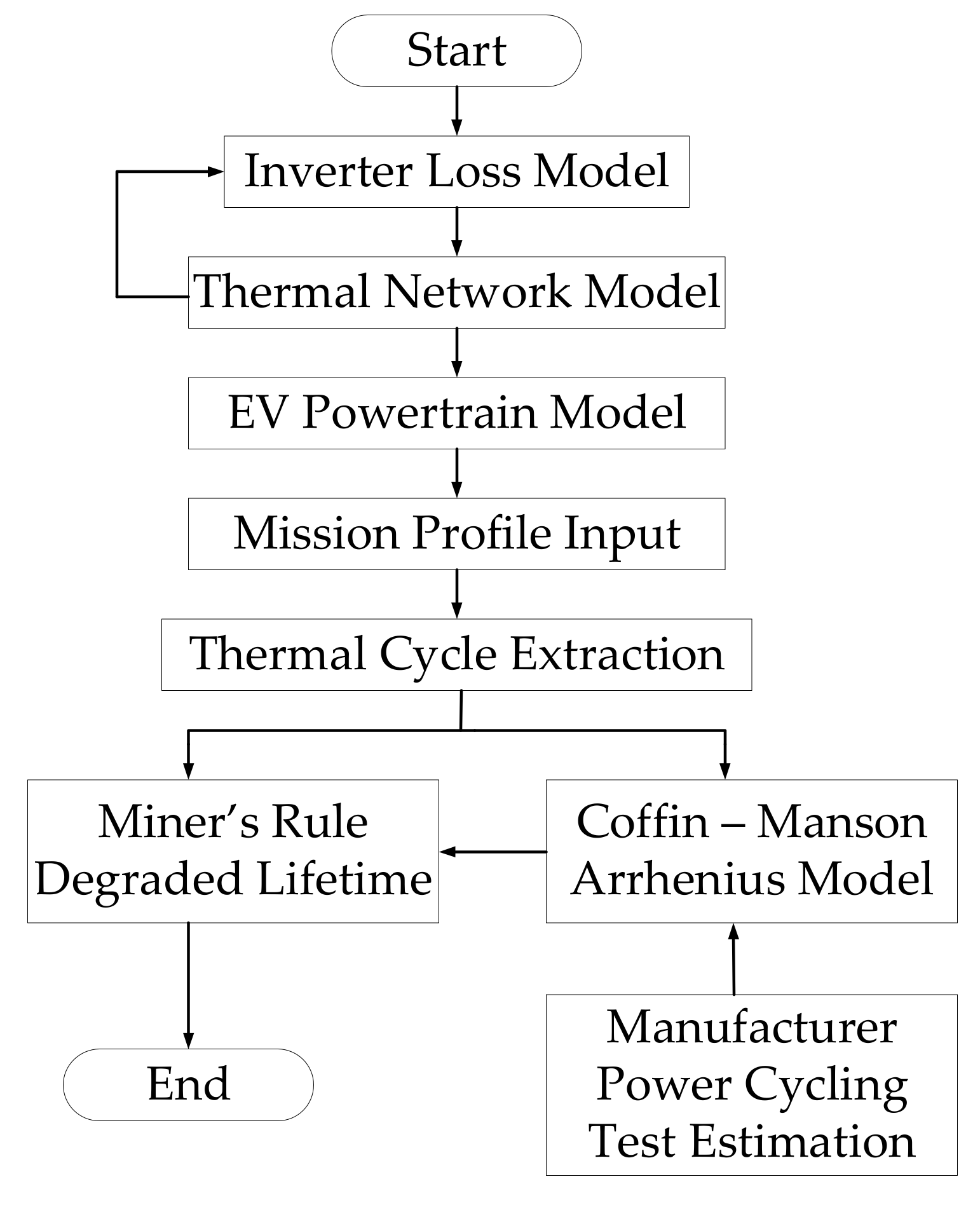
Figure 1. Flowchart of the proposed lifetime estimation procedure.
Vehicles 02 00022 g001
Figure 2. Circuit diagram and device characteristics for parameter extraction towards inverter power loss model, (a) V–I characteristics of IGBT and diode, (b) energy dissipation curves for diode and IGBT, and (c) Circuit diagram considering terminal parasitics.
Vehicles 02 00022 g002
Figure 3. Inverter hardware and IGBT power module layout considered in this paper. (a) Inverter DPT circuit diagram, (b) 100kW traction inverter.
Vehicles 02 00022 g003
Figure 4. Temperature properties of IGBT model. (a) heat flow direction from the chip to heatsink, and (b) thermal impedance of inverter module components.
Vehicles 02 00022 g004
Figure 5. Inverter RC thermal network model.
Vehicles 02 00022 g005
Figure 6. Cycle counting with Rainflow algorithm based on sample data, (a) sample temperature profile, (b) number of cycles counting.
Vehicles 02 00022 g006
Figure 7. Rainflow based cycle counting for selected mission profiles, (a) urban drive cycle, (b) WLTC3 drive cycle, (c) number of cycles for UDDS, and (d) number of cycles for WLTC3.
Vehicles 02 00022 g007
Table 1. Inverter parameters.
ModelDevice Parameters
Vce1200 V
Ic556 A
Max. Tj175 °C
IF438 A
Rce2.3 mΩ
Vge(th)5.8 V
ton276 ns
toff538 ns
Table 2. Parasitic elements used to model inverter transient response.
ModelDevice Parameters
cies26.4 nF
coes1.74 nF
cres1.41 nF
Ls/p15 nH