1. Introduction
Electronics are used in the mobile environment with increasing frequency for research, navigation and guidance, geographic information system functions (e.g., precision agriculture), and traditional functions (e.g., communications and entertainment). Automotive, agricultural, military, mining, and marine vehicles (hereafter mobile equipment) typically have a 12-volt direct current (12 VDC) power system. Mobile equipment 12 VDC systems are normally sufficient to power modern, high-efficiency electronics including personal computers, GPS units, data acquisition instruments, and the like. However, the electrical environment in which this mobile equipment operates is hazardous to delicate electronics, and has the potential to cause permanent damage. The most damaging over-voltage condition is caused by the industry known “load-dump”, which is a long duration (>500 ms) voltage spike (100–200 V) that is caused by high-energy load-dumps that are generated by the alternator when the battery is disconnected (through a loss or faulty connection, or accidental error during servicing) [
1,
2,
3,
4] (Kassakian, 1996; Shen, 2002; Jarvis, 2007; Eddleman 2017), Modern agricultural field research is dependent upon deploying numerous, custom sensing platforms ranging from plant health high-throughput-phenotyping systems to yield monitors to custom field and irrigation sensing systems. In many of these systems, expensive and custom electric sensors are deployed on mobile platforms that would benefit from circuit protection from surges.
Figure 1 shows a picture of one such custom system that is designed for harvesting research in cotton. The system accepts cotton dumps from research plots harvested with a commercial cotton stripper harvester. It then packages the harvested seed cotton into micro-modules, and weighs the modules. The system is powered by an electrical generator and, thus, is a sensitive and expensive weighing system that would benefit from an extended life, of which would likely be provided if it was protected from surges. Furthermore, accuracy of the sensing equipment is compromised when the power provided to it is noisy. Hence, there is a two-fold benefit of power protection; higher accuracy of data and the extended life of sensors.
A wealth of information is available for hardening electronics that will be used in the mobile equipment environment. Mobile equipment manufacturers have enacted standards [
5,
6,
7,
8,
9,
10,
11,
12] for vendors supplying electronic products. These standards provide guidance for designing and testing custom protection circuits. Because this is typically done for mass-produced products, intended for the automotive industry standards for standalone devices, to protect electronics on mobile farm equipment, are not generally available. Furthermore, most circuit designs provided by semi-conductor manufacturers, such as is discussed in [
4], are typically targeted at low-current devices and are frequently not suited for whole system designs, which include personal computers (PC), data acquisition systems, and touch-screen displays, as this type of system greatly exceeds the current capacity of these systems. Even when these types of systems can be adopted, they are typically only available in high-density surface-mount devices, and require expensive fabrication and long-lead times to obtain. In contrast, surge protection devices for 120 VAC systems that are readily available for consumer and industrial use are not suited for deployment into 12 VDC systems (e.g., the primary power source in farm tractors). Due to the lack of available mobile 12 VDC external protective equipment, installing an electronic device that was not designed for the mobile environment on a vehicle presents the risk that it may be damaged, and/or necessitates the fabrication of a complex circuit to protect it.
This paper presents an inexpensive circuit design that can protect electronics from three common hazards found in the mobile environment: Automotive load-dump voltage surges, electrical fast transients, and electrostatic discharges. This novel circuit possesses a simple design that does not require a circuit board, and can be fabricated using readily available off-the-shelf components.
2. Materials and Methods
2.1. Background
The International Electrotechnical Commission (IEC) is one of the world’s leading publishers of international standards for electrical and electronic technologies. Their standard IEC 61000 defines a set of electromagnetic immunity requirements that provide varying protection levels depending upon the severity of an application. It also provides a sound basis for the design of electrical and/or electronic devices so that they meet electromagnetic compatibility (EMC) requirements. These proactive guidelines reduce the risk of a product under development failing to meet specific standards or regulations. They limit electromagnetic disturbances emitted by a device and ensure that the device will be immune to the electromagnetic disturbances present in its environment (IEC, 2013). Regarding testing for immunity to mobile equipment electrical disturbances, their pertinent standards are:
IEC 61000-4-2 ESD [
5] (electro-static discharge) immunity test,
IEC 61000-4-4 EFT [
6] (electrical fast transients) immunity test,
IEC 61000-4-5 [
7] (load-dump surge) immunity test (IEC, 2005).
2.2. Electro-Static Discharge
Electro-static discharges (ESDs) can occur in dry environments that have below 20% relative humidity. Typical ESDs have rise times less than 10 ns, reach a peak voltage between 2000 and 30,000 V, and deliver 5 to 10 amps or more of current. Due to the short duration, the actual energy is low. However, ESD damage to electronic components is common due to high voltages and peak currents. Operational amplifiers, diodes, film resistors, integrated circuit chips, and other semi-conductors can be damaged by spikes as low as 200 to 2000 V. For this reason, component manufacturers increasingly include built-in protection. Unfortunately, even built-in protection is not adequate to protect against damage that human body static discharges may cause [
8] (DOD, 2010), which means that modern devices, as a result, usually have added protection circuits as well.
IEC 61000-4-2 [
5] specifies four levels of protection, as seen in
Table 1. It is not unusual for a data sheet to state that a component or product satisfies IEC 61000-4-2 [
5], while omitting to state at which level. In which case the safe assumption is that it only satisfies level-1, which is little better than what is already built into many semi-conductor chips (microcontrollers, analog to digital converters, amplifiers, etc.). It is prudent to verify that any component under consideration satisfies level-4 IEC 61000-4-2 [
5] specifications.
2.3. Electrical Fast Transients
Electrical fast transients (EFTs) result from switch contact bounce or are generated by the switching of inductive loads, such as motors and coils. These are particularly important to electronics designed for mobile equipment applications because these events will be encountered numerous times over the life of a vehicle. IEC 61000-4-4 [
6] EFT protection level definitions, in all cases, specify 5 ns to peak, 50 ns duration/peak, a total duration of 15 ms (2.5–5 kHz) with an off time of 300 ms; typical energy per pulse = 4 mJ, with typically 100–200 pulses emitted per burst (
Table 2).
Relevant test methods to determine electrical fast transient immunity can also be found in mobile equipment manufacturer publications such as Ford Motor Company’s EMC-CS-2009 [
9], the Society of Automotive Engineers’ Standard J1455 [
10], and International Standards Organization’s ISO 7637-3 [
11].
2.4. Load-Dump Surge
While electro-static discharges and electrical fast transients have similar profiles, and therefore can be guarded against with similar circuitry, the third class of mobile equipment disturbance is unique. The long duration load-dump surge threatens to cause catastrophic damage because it delivers the most energy. The load-dump surge has three common causes:
During ignition, the vehicle starter motor is drawing in excess of 200 amps. As soon as it is switched off, a back-EMF pulse out of the inductor creates a large load-dump.
Vehicle lights, especially on harvest equipment with a wide illumination field, similarly create a surge in the vehicle 12 VDC system when they are switched off. This is because the alternator controller cannot respond instantly to a sudden decrease in demand, which results in a temporary over voltage event.
Though occurring less frequently, the greatest load-dump is caused when the battery cable comes loose while the motor is running; this worst-case scenario may result in a 120 V, 400 ms load-dump event [
2,
3].
The IEC test designed to confirm immunity to a load-dump surge, in all cases, involves an 8/20 μs pulse, which is defined as 8 μs rise-time to peak, followed by decay to 50% peak height duration at 20 μs. The voltage peaks corresponding to each level of protection are presented in
Table 3.
Relevant test methods to determine automotive load-dump immunity can also be found in mobile equipment manufacturer publications such as Ford Motor Company’s EMC-CS-2009 [
9], the Society of Automotive Engineers’ Standard J1113 [
12], and International Standards Organization’s ISO 7637-2 [
5]. A patent was issued for a method to protect electronics from a load-dump [
13]. However, off-the-shelf load-dump protection devices for 12 VDC vehicular applications are not generally available in the consumer market.
2.5. Available Components
Two available surge protection components suitable for ESD and EFT protection of mobile equipment are:
TVS (transient voltage surge) diodes: TVS diodes have a rapid 10 ps or less turn on time and typically protect against ESDs and EFTs to IEC 61000-4-5 level-4 [
7]. Available in surface-mount components, TVS diodes are the least expensive protection components. Allowable TVS peak pulse power depends on pulse duration. For example, a TVS diode providing protection to 5000 W for a 0.1 μs pulse only provides 20 W of protection for a 10 ms duration pulse. TVS diodes provide low energy (less than 0.01 J), short duration ESD protection up to 8000 V. However, they are not suitable for long duration high-energy pulses, such as is typical for load-dumps.
MOV/MLV (metal-oxide varistor/multi-layer varistor): MOVs are high surge variants of transient voltage surge diodes. In surface-mount packages they can dissipate upwards of 10 to 25 J, with peak currents of 1000 A or more for typical 8/20 μs pulses. Another advantage is their rapid response. MOVs also provide short duration ESD protection up to 8000 V. Similar to TVS diodes, they are not suitable for load-dump protection.
While many options are available for surge protection for 120–440 VAC applications, and some options exist to protect lower voltage equipment from ESDs and EFTs, there are no options available that will provide the sufficient load-dump protection that is required on mobile equipment. The lack of available devices led to the development of the reported protection circuit.
2.6. Protection Circuit Design Criteria
Since load-dump events have the potential to deliver the most energy and cause the most severe damage to electrical and electronic devices on mobile equipment, it is protection from this type of surge that governs the design of a protection circuit. Load-dumps can be 200 to 400 ms in duration, and can reach 80 to 120 VDC. The objective was to protect a PC and LCD screen, drawing 4 amps with an input range of 6 to 34 VDC, and a LIN-bus node, drawing 70 mA with an input range of 8 to 40 VDC.
2.7. Design Process
The open-source electronic simulation software program SPICE [
14] (Simulation Program with Integrated Circuit Emphasis, Electronics Research Laboratory, University of California, Berkeley) is an industry-standard method for verifying circuit operation at the transistor level before committing to manufacturing an integrated circuit. The software also does a good job of modeling non-linear board circuits. SPICE is reliable enough that integrated-circuit, IC, designers trust it; they use SPICE instead of prototyping when they create complex chips, going straight from SPICE to manufacturing [
14,
15,
16,
17,
18].
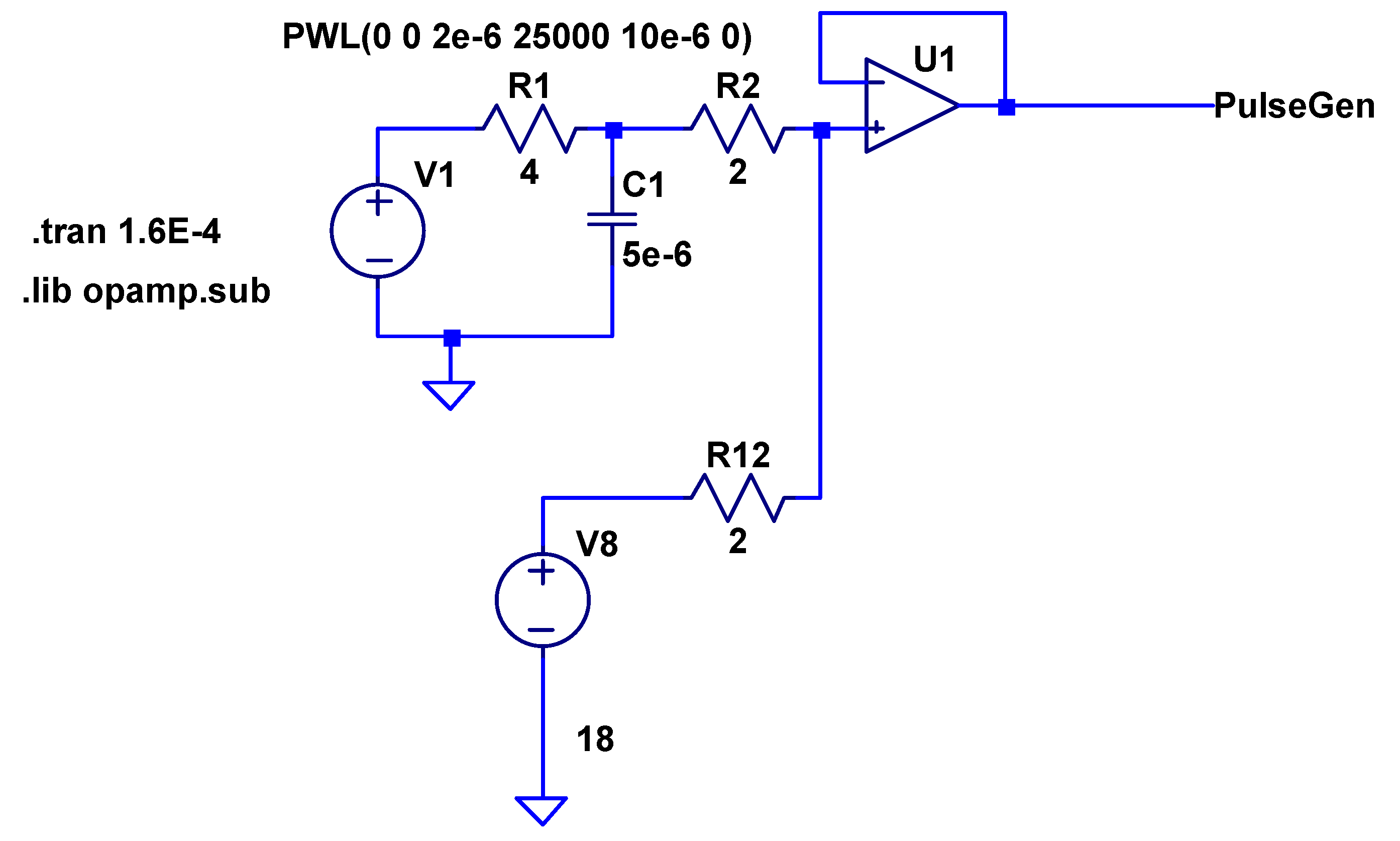
The first task was to reproduce the typical ESD, EFT, and load-dump surge pulses that the electronics on mobile equipment are required to survive. The built-in piece-wise-linear, PWL, function in SPICE, with the addition of a few components and a buffer, provided a high-quality pulse generator independent of the downstream circuitry. The generator is depicted in
Figure 2, along with the SPICE simulation commands, in dot notation [
15]. As semiconductors are highly non-linear, simulations can produce different answers depending on the integration routine that is utilized. To ensure accuracy, each simulation was performed using at least two different integration techniques for comparison. The two main comparison integration routines utilized for comparison were: “Gear” and the “Modified Trapezoidal” routines that are built into SPICE [
15,
16,
17].
2.8. Experimental Design
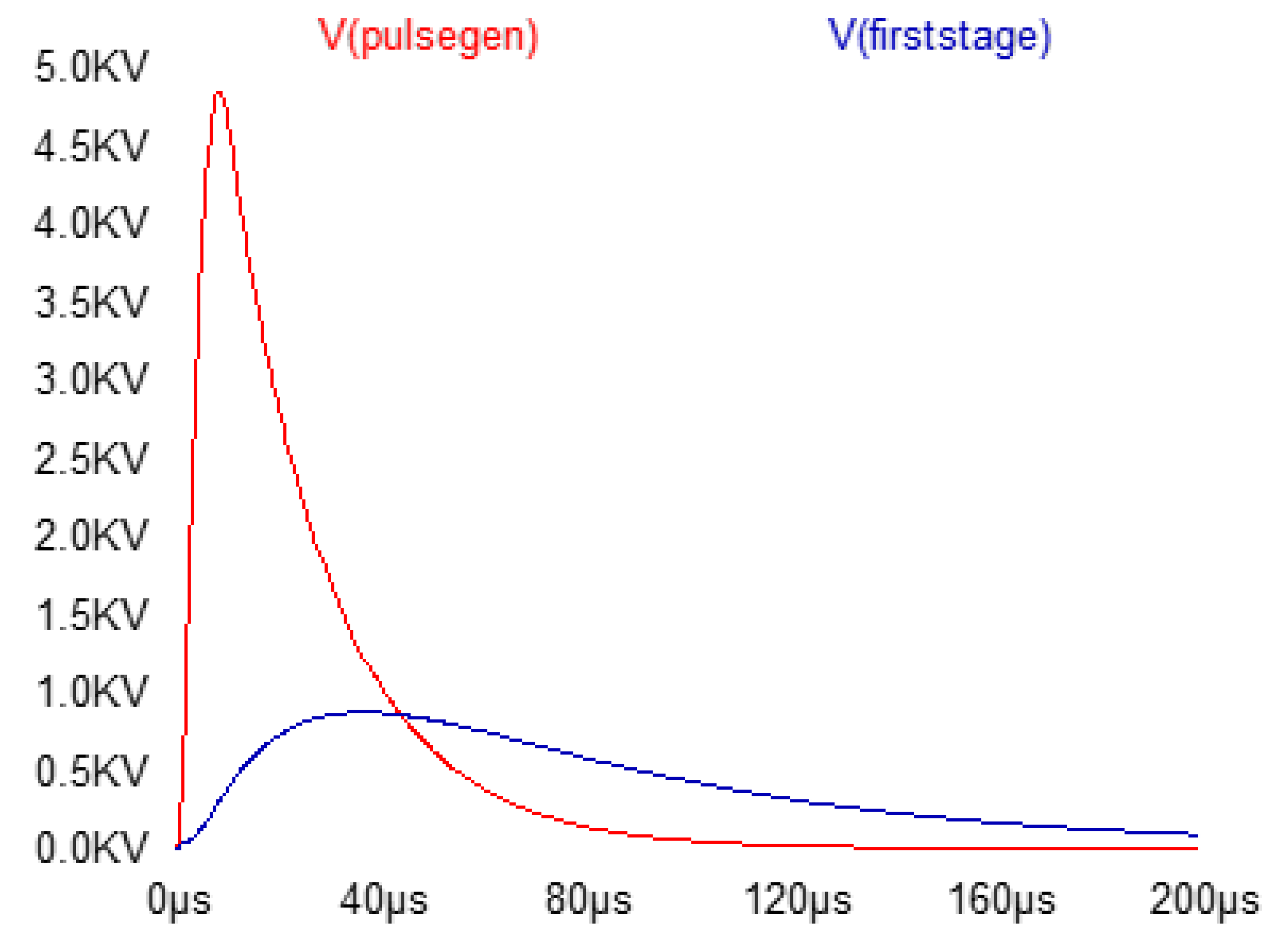
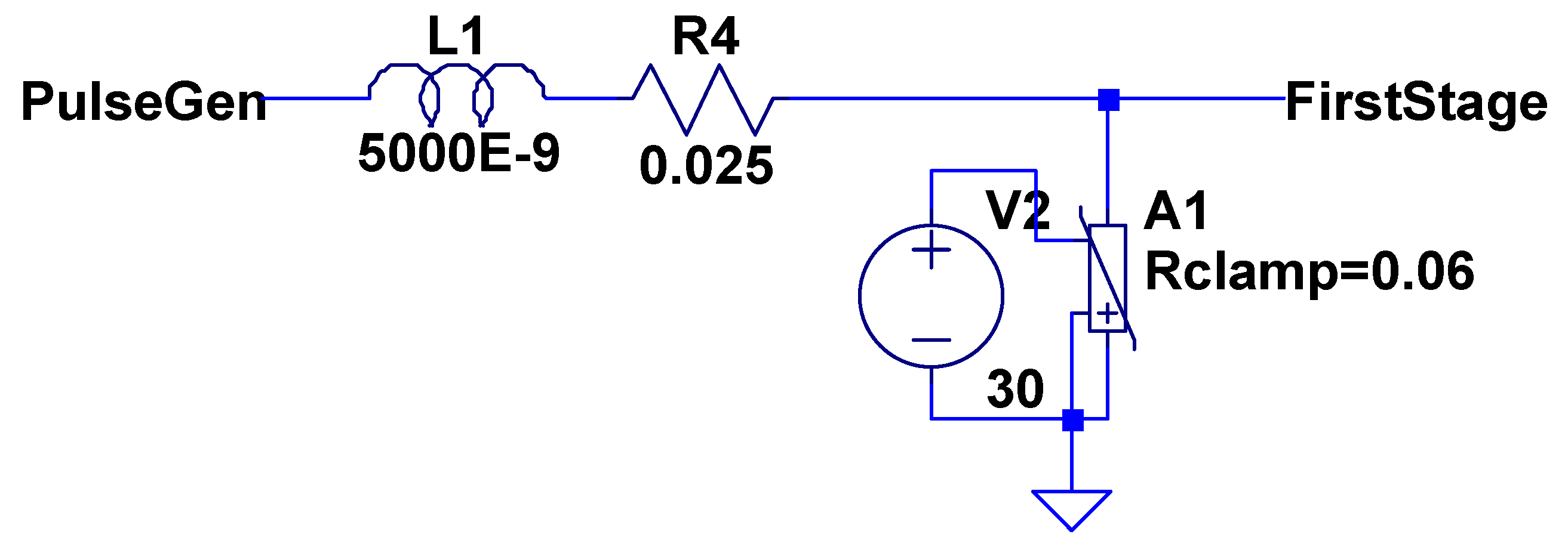
To explore the possible circuits, simulations were run that included the impedance of 3 m of 18-gauge cable, between the alternator and the test circuit, which was represented by an inductance (L1) and a resistance (R4) (
Figure 3). Several iterations with a single varistor (variable resistor) indicated that a single stage configuration was not sufficient to ensure that the input voltage to the PC stayed below 34 V. Additional iterations with a second stage varistor improved the response and resulted in a circuit that provided immunity to an IEC 61000-4-4 [
6] level-4 fast transient (2000 V, 5/50 ns), but not to an IEC 61000-4-5 [
7] level-4 load-dump (4000 V, 8/20 μs), nor to industry defined load-dumps (60–120 V peak, 100–400 ms duration, comprising 40–80 J) [
2,
3,
4,
7]. The simulation results of the single varistor protection circuit are detailed in
Figure 3.
Figure 4 details the output from the pulse generator.
The lack of full compliance in our initial circuit designs led to a deeper literature search. In the proceedings of an Automotive EMC conference [
3], a few approaches of interest were presented for meeting load-dump requirements. However, when one approach was simulated, the reported circuit was found to have the adverse effect of turning off the protected device, a situation that is unsuitable for many research applications, including those of the authors. To meet the stricter criteria, more customs designs were explored iterating upon existing and new approaches.
3. Results
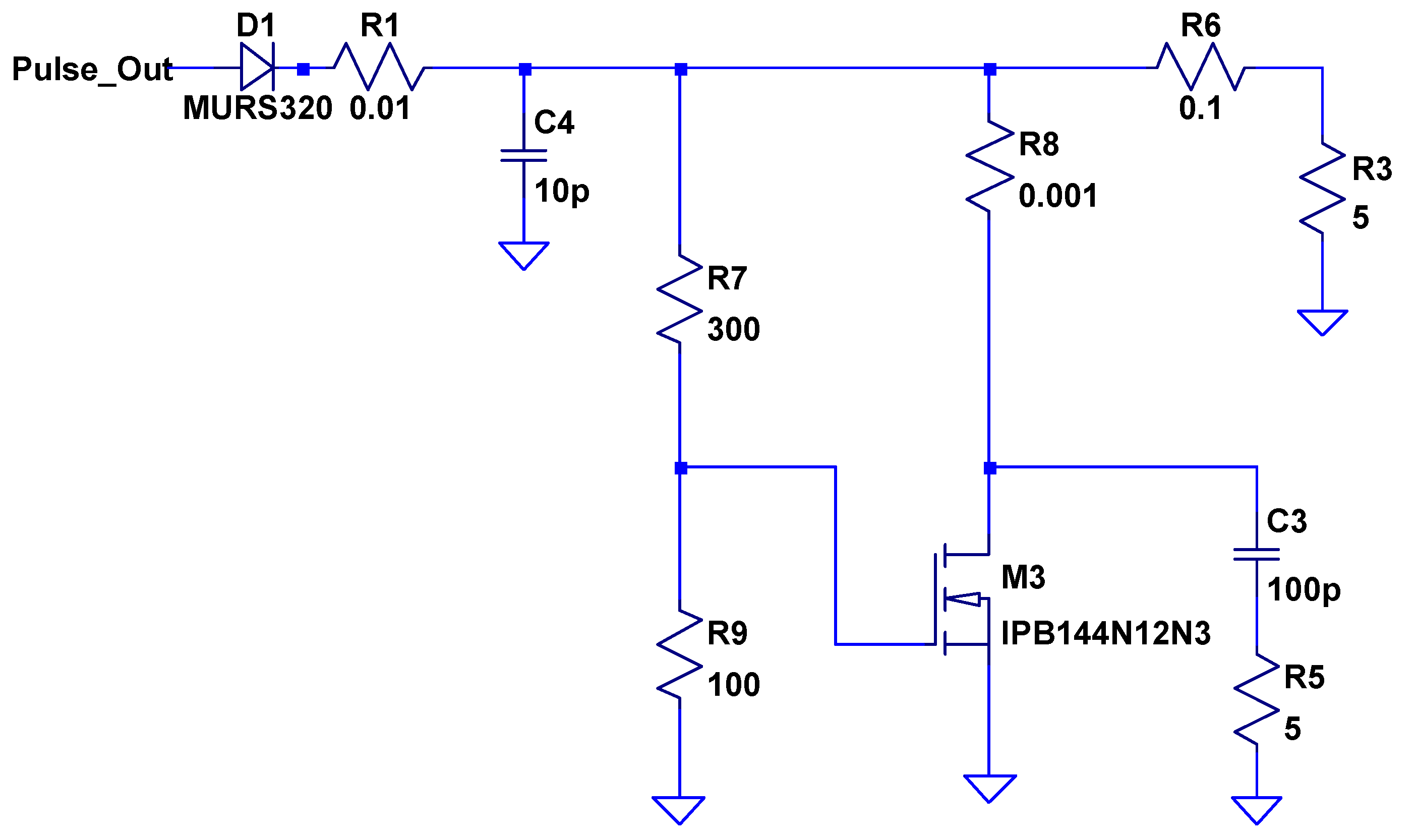
The final circuit design did not require a circuit board and could be put together using an off-the-shelf module level power metal-oxide-semiconductor-field-emission-transistor, MOSFET, that, for a nominal cost, can readily absorb 100 to 200 J at voltage levels in excess of 200 V, which is more than sufficient for even the most energetic load-dump. The final optimized circuit is detailed in
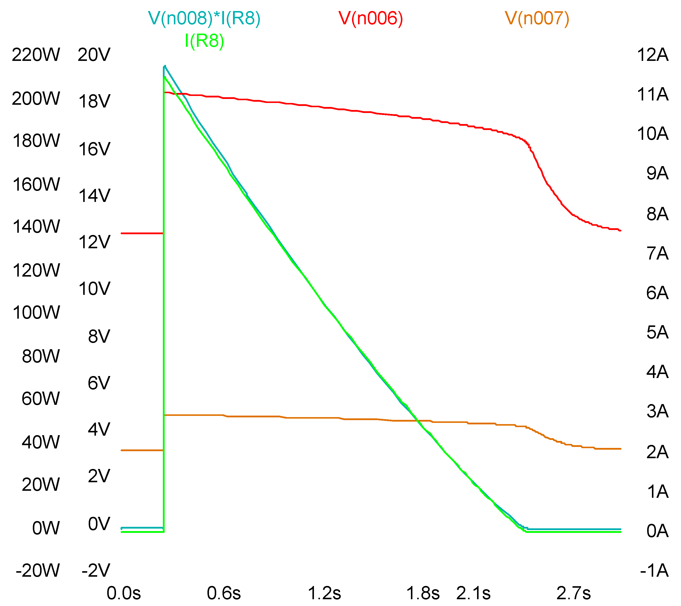
Figure 5. The load-dump disturbance is shown in
Figure 6.
Figure 7 shows the volt amps and current through resistor-8 decaying over 2 s (node 008). It also shows a safe voltage level at the protected electronics (node 006, after R6). Voltage node V(n008)*I(R8) is power through the MOSFET, where I(R8) is current through resistor R8 and V(n006) is voltage at the final load resistor R3 (the protected system). Of importance is that the impulse was spread-out from less than 200 ms to over 2 s, thereby reducing the 62 V equipment-damaging peak to a safer 19 V. This modest 6.5 V over normal input voltage is easily handled by readily available DC–DC converters or typical automotive-class linear voltage regulators.
These results illustrate how a damaging 180 J load-dump pulse can be smoothed and significantly reduced in power by shunting the pulse energy to ground through a power MOSFET. The automatic stabilization of the circuit allows for the voltage to slowly descend back to normal operating levels, without interruption, after only a modest rise from 12.5 to 19 V. Typical off-the-shelf DC–DC converters and linear power regulators are designed to operate up to 25 V without damage. A 200 V power MOSFET rated at twice the expected power is recommended, because the average energy dissipated is equal to half of the energy in the pulse, and can be obtained for less than $20 US.
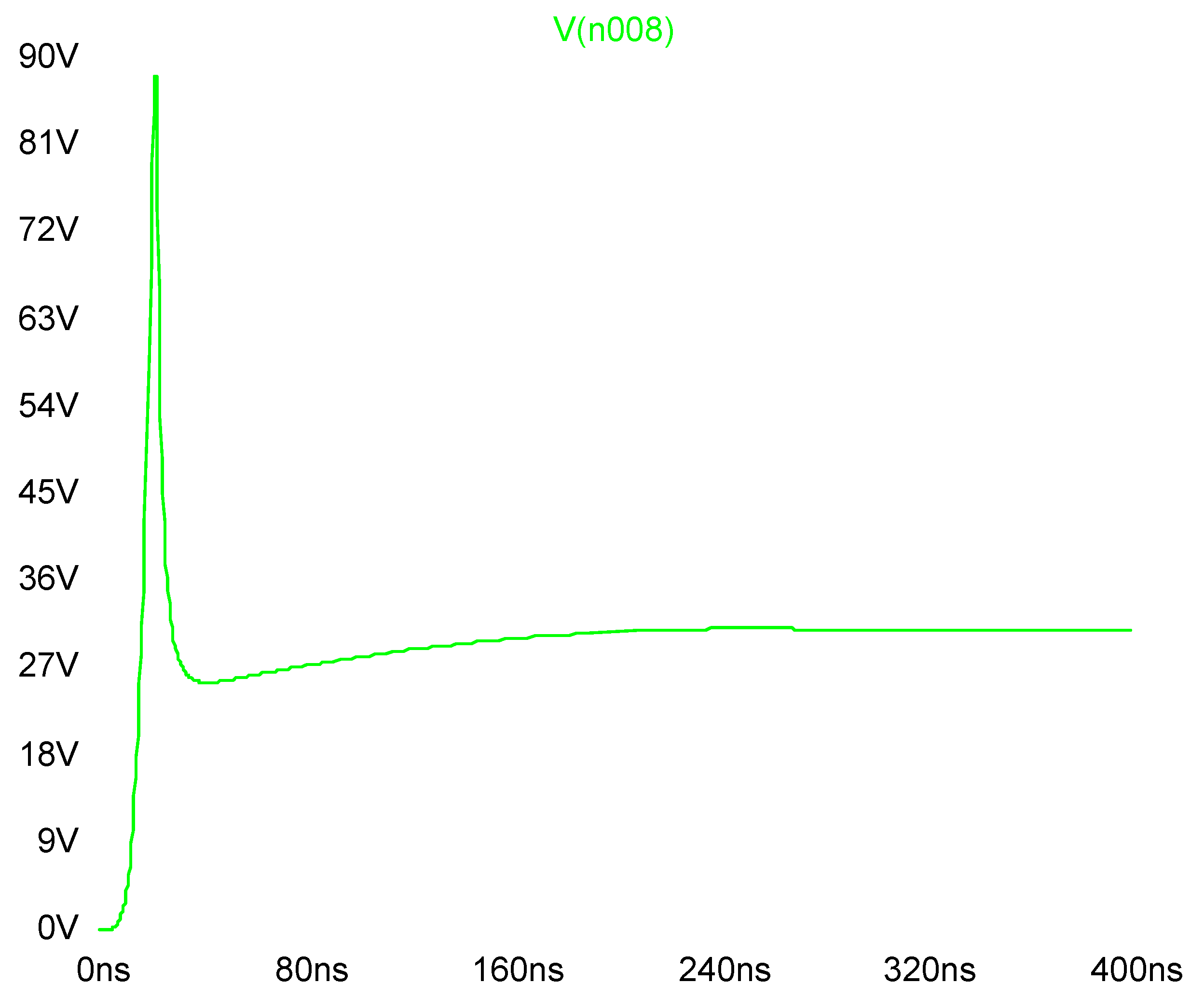
The proposed MOSFET shunt protection circuit was tested for immunity to ESDs and EFTs by modifying the original pulse generation test circuit,
Figure 1, to achieve a pulse input for a 4000 V, 200 ns pulse. With the MOSFET shunt protection circuit, the 4000 V spike was filtered to a manageable 90 V short duration impulse,
Figure 8. A final simulation that added a simple R–C filter at the load site was found to be sufficient to remove the low-energy short-duration 90 V spike that passed through the power MOSFET protection stage.
The MOSFET load-dump protection circuit attenuated the EFTs to a level easily filtered with a 0.1 Ω resistor and a 10 uF capacitor. The addition of the 10 uF capacitor reduced the EFTs to 30 V with an 80 us duration. This resulted in a pulse of 100 pico-Joules of energy. Thus, any standard TVS diode could be added to safely remove this low-power pulse input without risk to the TVS diode. This was confirmed by adding both the capacitor and the TVS diode to the original MOSFET protection circuit of
Figure 2. SPICE results indicated a total current through the TVS diode less than 400 nA for the ISO 7637-2 [
10] Test Pulse 5 load-dump input.
4. Discussion
The most challenging electronic disturbance requiring a protective device was the 80 V, 400 ms duration load-dump. A power MOSFET-based shunt circuit was developed to dump the main long duration power to ground and extend the pulse from 400 ms to over 2 s. This allowed the voltage to be reduced from 80 V to less than 20 V, a level easily managed by readily available off-the-shelf DC–DC converters. Since 200 V power MOSFET modules that handle 500–1000 W are easily sourced, there is a readily available supply of modules, with excess capacity, that can handle well over the voltage and energy requirements of this application.
A second stage was added to handle rapid high-voltage ESD and EFT disturbances. Given the very short duration of these types of events, it was shown that a simple, readily available TVS diode, coupled with a 10uF capacitor, could provide sufficient second stage protection. The TVS diode was shown to be capably protected by the MOSFET shunt circuit. This novel two-stage circuit was shown to provide immunity for electronics, such as a PC-based distributed data acquisition system on mobile equipment. This design provides the necessary level of protection to meet IEC 61000-4-2, IEC 61000-4-4, and IEC 61000-4-5 [
5,
6,
7] requirements for providing protection at the highest levels; as suggested in testing standards and literature reports AEC Q-200-007 [
19,
20,
21] Pulse 5 load-dump high energy inputs. Designing the protection circuit in two stages protects the more sensitive analog circuit components from the harsh mobile equipment environment. This novel MOSFET shunt design can be easily assembled, as it only has a power MOSFET module and a few resistors and, thus, there is really no need for a circuit board; although, a circuit board is convenient if packaging into a compact box. In which case, as all the components can be sourced in either through-hole or large-pitch surface-mount components, fabrication is again readily achieved; something that cannot be said for offerings from the typical solutions by semi-conductor manufactures, as invariably they are all provided on very small pitch surface-mount form-factors only, which are very difficult to solder by hand and are best left for robotic assembly. As such, these solutions are not readily available for the typical research and development shop.
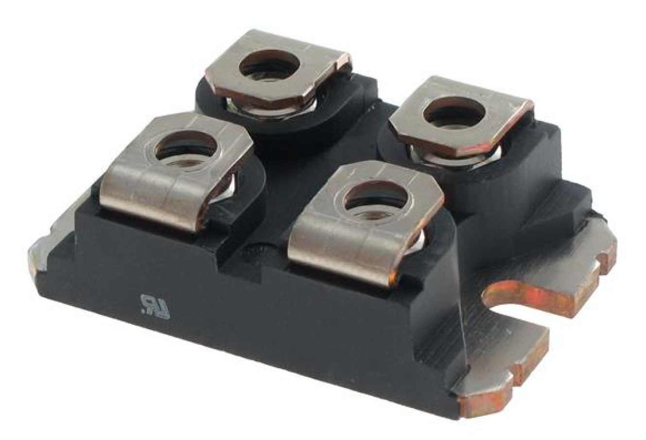
For use in rapid construction with off-the shelf components, the power MOSFET MSC080SMA120J or VS-FB190SA10 are two of many power MOSFETs that are suitable for such use,
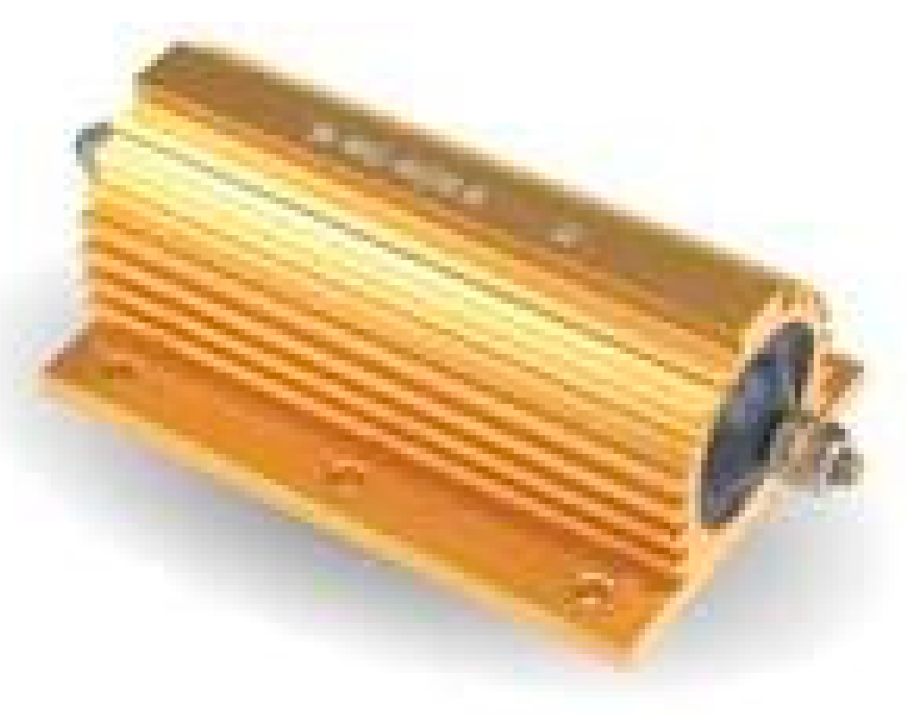
Figure 9. These types of MOSFETs are typically rated at >1200 V, with an on-resistance of 100 m Ohms, and are available in a SOT-227 industry standard package that is easily hooked up to with the built-in screw terminals (thereby alleviating the need for a printed circuit board). The SOT-227 package is also capable of sinking 100’s of amps, which affords the energy-sink capacity needed to absorb transient vehicular load-dump situations. For example, the VS-FB190 is rated at 190 amps continuous duty cycle at 40 °C. For long duration 100–200 V load-dumps, this package provides the energy sinking capacity of 40 kW and thereby avoids the need for the manufacture of a printed-circuit-board, PCB. All that is left to complete the circuit are a few power resistors, which also come in easy-to-mount packages and are readily available in 100 W packages,
Figure 10. Of note is that the power resistors were only selected due to a need for the avoidance of circuit board mounting, as, usually, such power resistors have built-in screw holes that are designed for mounting on a simple plate. Suitable, and applicable, resistors to use are the AH series power resistors that are available from Vishay. These resistors are rated to >1200 V continuous with a peak rating of 5000 V. Because, in normal use, the resistors only provide a biasing function, the current through them can be minimal and can be sized appropriately to avoid an over-power condition when in conduction-mode during a load-dump. As load-dumps range from 100–200 V, the worst-case use would see a 400 V drop across both resistors (400 Ohms), which in turn would create a maximum current through each resistor of 1 amp. This 1 amp load would require a power absorption requirement, for 300 Ohm R7, of 300 W; but as it would be less than 1 s in duration, a 300 W version, such as Vishay’s AH300, could easily absorb the elevated power for as long as it needs to. Similarly, an AH100 would be suitable for the R9, 100 Ohm, resistor. If a smaller wattage resistor was desired, to form a more compact solution, simply increase the resistor values in ratio to limit current accordingly.
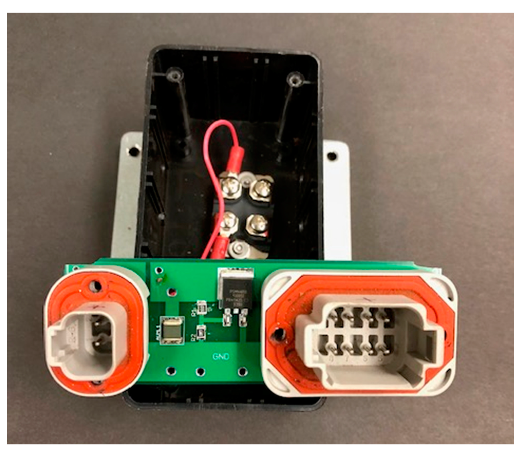
Another, more compact, option would be to use through-hole protoboard or large pitch surface-mount components, and have a printed-circuit-board fabricated that can be easily hand-soldered.
Figure 11 shows this implementation using a large pitch surface-mount design. The bottom of the PCB board is a flood-filled ground plane. The puck in the bottom of the box is an added diode rectifier, which is in same location as diode D1 that is detailed in
Figure 5, in a SOT-227 package, that is used to provide added protection against reverse polarity hook-ups. The connectors mounted on the PCB board are water-tight Deutsch connectors. On the PCB circuit board are the biasing resistors R7, R9 and the power MOSFET M3. The artwork for the PCB board is shown in
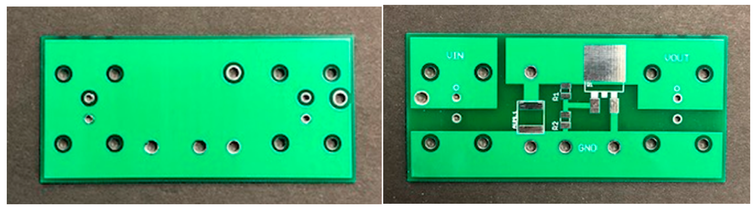
Figure 12.


