
Surface Characteristics and Performance Optimization of W-Doped Vanadium Dioxide Thin Films


Abstract
1. Introduction
2. Materials and Methods
2.1. Experimental Design
2.2. Thin-Film Deposition
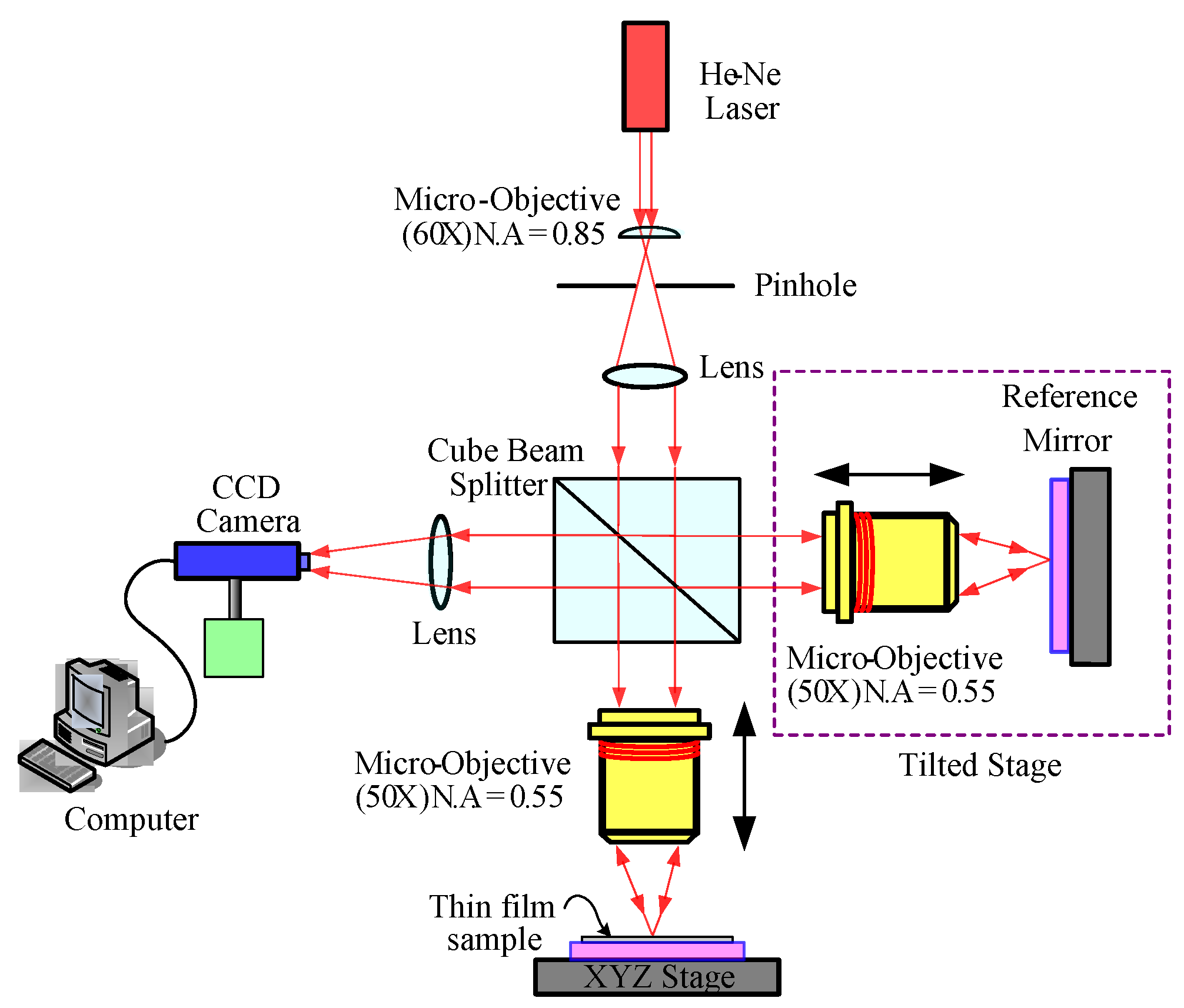
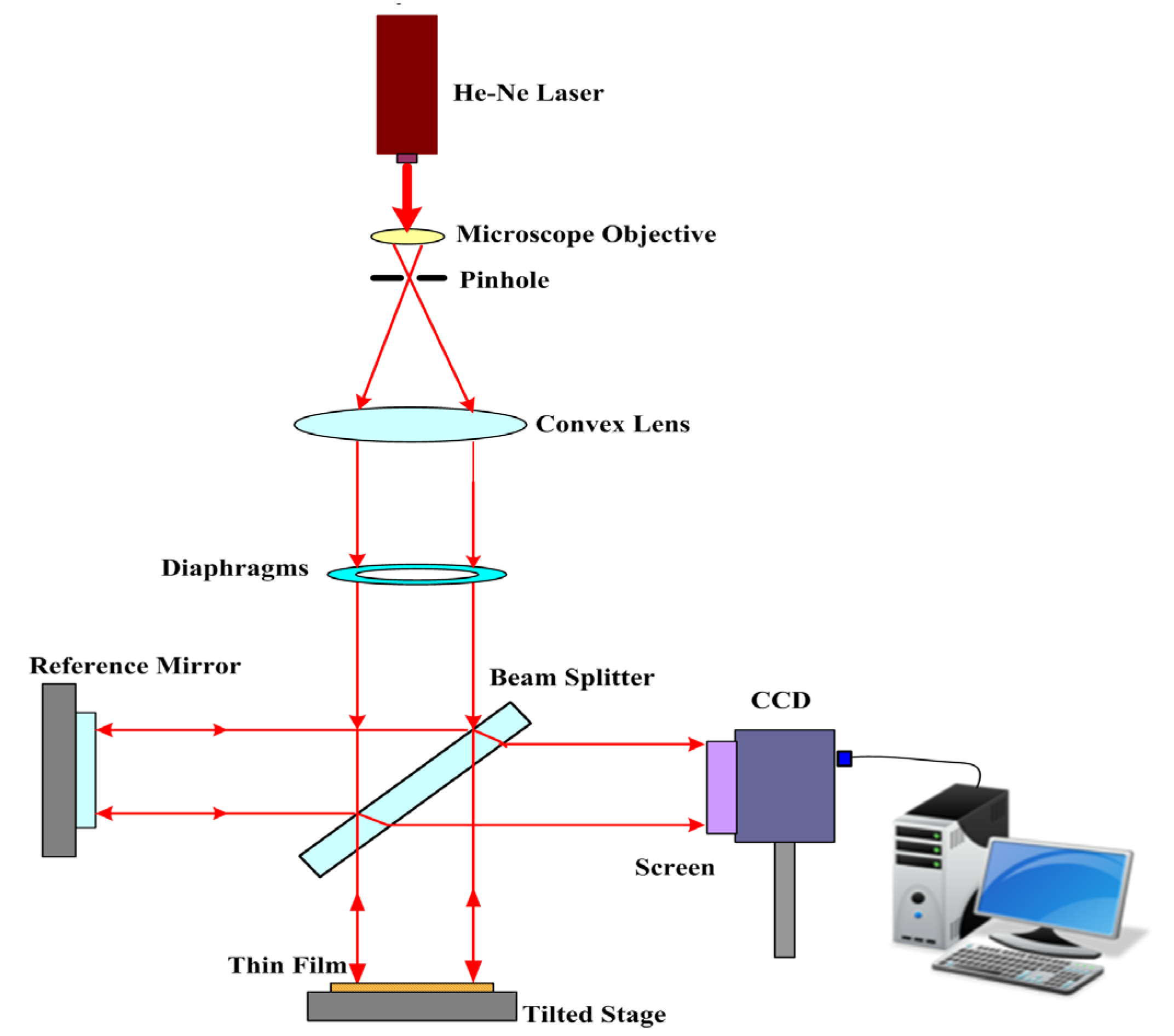
2.3. Measurement Methods
2.4. Signal-to-Noise Ratio
3. Results and Discussion
4. Conclusions
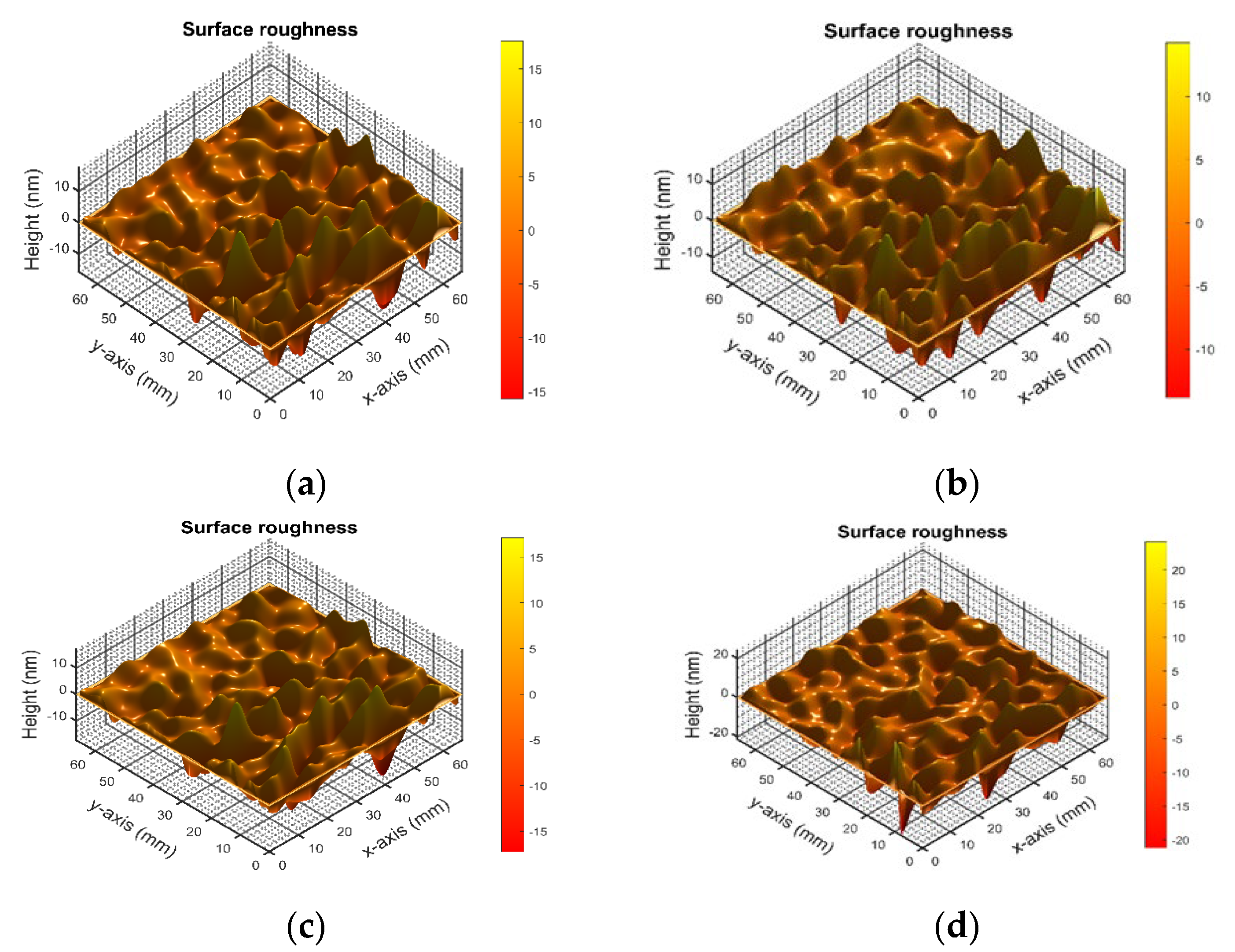
- When the oxygen flow rate is 60 sccm, the heating temperature is 280 °C, the film thickness is 60 nm, and the VO2 is doped with 3% tungsten, the VO2 thin film exhibits the lowest surface roughness of 2.12 nm.
- Under conditions of 20 sccm oxygen flow rate, 265 °C heating temperature, 120 nm film thickness, and 5% tungsten doping, the VO2 thin film shows the lowest residual stress of −0.195 GPa.
- Under conditions of an oxygen flow rate of 0 sccm, a heating temperature of 280 °C, a film thickness of 60 nm, and a 5% tungsten doping, the VO2 thin film achieves the highest visible light transmittance of 64.33%.
- When the oxygen flow rate is 60 sccm, the heating temperature is 295 °C, the film thickness is 150 nm, and the tungsten doping is 5%, the VO2 thin film exhibits the lowest infrared transmittance of 31.34%.
Author Contributions
Funding
Data Availability Statement
Acknowledgments
Conflicts of Interest
References
- Shen, N.; Chen, S.; Huang, R.; Huang, J.; Li, J.; Shi, R.; Niu, S.; Amini, A.; Cheng, C. Vanadium dioxide for thermochromic smart windows in ambient conditions. Mater. Today Energy 2021, 21, 100827. [Google Scholar] [CrossRef]
- Jung, K.H.; Yun, S.J.; Slusar, T.; Kim, H.T.; Roh, T.M. Highly transparent ultrathin vanadium dioxide films with temperature-dependent infrared reflectance for smart windows. Appl. Surf. Sci. 2022, 589, 714–721. [Google Scholar] [CrossRef]
- Cui, Y.; Ke, Y.; Liu, C.; Chen, Z.; Wang, N.; Zhang, L.; Zhou, Y.; Wang, S.; Gao, Y.; Long, Y. Thermochromic VO2 for energy-efficient smart windows. Joule 2018, 2, 1707–1746. [Google Scholar] [CrossRef]
- Jin, P.; Xu, G.; Tazawa, M.; Yoshimura, K. Design, formation and characterization of a novel multifunctional window with VO2 and TiO2 coatings. Appl. Phys. A 2003, 77, 455–459. [Google Scholar] [CrossRef]
- Granqvist, C.G. Window coatings for the future. Thin Solid Film. 1990, 193, 730–741. [Google Scholar] [CrossRef]
- Kang, S.K.; Ho, D.H.; Lee, C.H.; Lim, H.S.; Cho, J.H. Actively operable thermoresponsive smart windows for reducing energy consumption. ACS Appl. Mater. Interfaces 2020, 12, 33838–33845. [Google Scholar] [CrossRef]
- Vernardou, D.; Pemble, M.E.; Sheel, D.W. The Growth of Thermochromic VO2 Films on Glass by Atmospheric-Pressure CVD: A Comparative Study of Precursors, CVD Methodology, and Substrates. Chem. Vap. Depos. 2006, 12, 263–274. [Google Scholar] [CrossRef]
- Gagaoudakis, E.; Aperathitis, E.; Michail, G.; Kiriakidis, G.; Binas, V. Sputtered VO2 coatings on commercial glass substrates for smart glazing applications. Sol. Energy Mater. Sol. Cells 2021, 220, 110845. [Google Scholar] [CrossRef]
- Zhang, J.; Li, J.; Chen, P.; Rehman, F.; Jiang, Y.; Cao, M.; Zhao, Y.; Jin, H. Hydrothermal growth of VO2 nanoplate thermochromic films on glass with high visible transmittance. Sci. Rep. 2016, 6, 27898. [Google Scholar] [CrossRef]
- Seyfouri, M.M.; Binions, R. Sol-gel approaches to thermochromic vanadium dioxide coating for smart glazing application. Sol. Energy Mater. Sol. Cells 2017, 159, 52–65. [Google Scholar] [CrossRef]
- Wang, S.; Owusu, K.A.; Mai, L.; Ke, Y.; Zhou, Y.; Hu, P.; Magdassi, S.; Long, Y. Vanadium dioxide for energy conservation and energy storage applications: Synthesis and performance improvement. Appl. Energy 2018, 211, 200–217. [Google Scholar] [CrossRef]
- Vu, T.D.; Chen, Z.; Zeng, X.; Jiang, M.; Liu, S.; Gao, Y.; Long, Y. Physical vapour deposition of vanadium dioxide for thermochromic smart window applications. J. Mater. Chem. C 2019, 7, 2121–2145. [Google Scholar] [CrossRef]
- Marszałek, K.; Winkowski, P.; Marszałek, M. Antireflective bilayer coatings based on AlO film for UV region. Mater. Sci.-Pol. 2015, 33, 6–10. [Google Scholar] [CrossRef]
- Yang, Z.; Ko, C.; Ramanathan, S. Oxide electronics utilizing ultrafast metal-insulator transitions. Annu. Rev. Mater. Res. 2011, 41, 337–367. [Google Scholar] [CrossRef]
- Chang, T.C.; Cao, X.; Bao, S.H.; Ji, S.D.; Luo, H.J.; Jin, P. Review on thermochromic vanadium dioxide based smart coatings: From lab to commercial application. Adv. Manuf. 2018, 6, 1–19. [Google Scholar] [CrossRef]
- Omer, A.M. Energy, environment and sustainable development. Renew. Sustain. Energy Rev. 2008, 12, 2265–2300. [Google Scholar] [CrossRef]
- Green, M.A. Photovoltaics: Technology overview. Energy Policy 2000, 28, 989–998. [Google Scholar] [CrossRef]
- Bhupathi, S.; Wang, S.; Ke, Y.; Long, Y. Recent progress in vanadium dioxide: The multi-stimuli responsive material and its applications. Mater. Sci. Eng. R Rep. 2023, 155, 100747. [Google Scholar] [CrossRef]
- Xu, S.; Ma, H.; Dai, S.; Jiang, Z. Study on optical and electrical switching properties and phase transition mechanism of Mo 6+-doped vanadium dioxide thin films. J. Mater. Sci. 2004, 39, 489–493. [Google Scholar] [CrossRef]
- Lopez, R.; Boatner, L.A.; Haynes, T.E.; Feldman, L.C.; Haglund, R.F. Synthesis and characterization of size-controlled vanadium dioxide nanocrystals in a fused silica matrix. J. Appl. Phys. 2002, 92, 4031–4036. [Google Scholar] [CrossRef]
- Liang, Z.; Zhao, L.; Meng, W.; Zhong, C.; Wei, S.; Dong, B.; Xu, Z.; Wan, L.; Wang, S. Tungsten-doped vanadium dioxide thin films as smart windows with self-cleaning and energy-saving functions. J. Alloys Compd. 2017, 694, 124–131. [Google Scholar] [CrossRef]
- Pan, M.; Zhong, H.; Wang, S.; Liu, J.; Li, Z.; Chen, X.; Lu, W. Properties of VO2 thin film prepared with precursor VO (acac)2. J. Cryst. Growth 2004, 265, 121–126. [Google Scholar] [CrossRef]
- Ji, H.; Liu, D.; Cheng, H. Infrared optical modulation characteristics of W-doped VO2 (M) nanoparticles in the MWIR and LWIR regions. Mater. Sci. Semicond. Process. 2020, 119, 105141. [Google Scholar] [CrossRef]
- Harrick, N.J.; Du Pre, F.K. Effective thickness of bulk materials and of thin films for internal reflection spectroscopy. Appl. Opt. 1996, 5, 1739–1743. [Google Scholar] [CrossRef] [PubMed]
- Tien, C.L.; Chiang, C.Y.; Lin, S.C. Optimization of Electron-Beam Evaporation Process Parameters for ZrN Thin Films by Plasma Treatment and Taguchi Method. Plasma 2023, 6, 478–491. [Google Scholar] [CrossRef]
- Dehnad, K. Quality Control, Robust Design, and the Taguchi Method; Springer Science & Business Media: Berlin, Germany, 2012. [Google Scholar]
- Barker, T.B. Engineering Quality by Design: Interpreting the Taguchi Approach; CRC Press: Boca Raton, FL, USA, 1990; Volume 113. [Google Scholar]
- Swanepoel, R. Determination of the thickness and optical constants of amorphous silicon. J. Phys. E Sci. Instrum. 1983, 16, 1214–1222. [Google Scholar] [CrossRef]
- Panjan, P.; Drnovšek, A.; Gselman, P.; Čekada, M.; Panjan, M. Review of growth defects in thin films prepared by PVD techniques. Coatings 2020, 10, 447. [Google Scholar] [CrossRef]
- Lukaszkowicz, K. Review of nanocomposite thin films and coatings deposited by PVD and CVD technology. In Nanomaterials; InTech: Houston, TX, USA, 2011; pp. 145–163. [Google Scholar]
- Tien, C.L.; Yang, H.M.; Liu, M.C. The measurement of surface roughness of optical thin films based on fast Fourier transform. Thin Solid Film. 2009, 517, 5110–5115. [Google Scholar] [CrossRef]
- Tien, C.L.; Yu, K.C.; Tsai, T.Y.; Lin, C.S.; Li, C.Y. Measurement of surface roughness of thin films by a hybrid interference microscope with different phase algorithms. Appl. Opt. 2014, 53, H213–H219. [Google Scholar] [CrossRef] [PubMed]
- Tien, C.L.; Lin, T.W.; Yu, K.C.; Tsai, T.Y.; Shih, H.F. Evaluation of electrical, mechanical properties, and surface roughness of DC sputtering nickel-iron thin films. IEEE Trans. Magn. 2014, 50, 1–4. [Google Scholar] [CrossRef]
- Tien, C.L.; Zeng, H.D. Measuring residual stress of anisotropic thin film by fast Fourier transform. Opt. Express 2010, 18, 16594–16600. [Google Scholar] [CrossRef]
- Takeda, M.; Ina, H.; Kobayashi, S. Fourier-transform method of fringe-pattern analysis for computer-based topography and interferometry. J. Opt. Soc. Am. 1982, 72, 156–160. [Google Scholar] [CrossRef]
- Takeda, M.; Mutoh, K. Fourier-transform profilometry for the automatic measurement of 3-D object shapes. Appl. Opt. 1983, 22, 3977–3982. [Google Scholar] [CrossRef] [PubMed]
- Tien, C.L.; Lee, C.C.; Tsai, Y.L.; Sun, W.S. Determination of the mechanical properties of thin films by digital phase shifting interferometry. Opt. Commun. 2001, 198, 325–331. [Google Scholar] [CrossRef]
- Puh, F.; Jurkovic, Z.; Perinic, M.; Brezocnik, M.; Buljan, S. Optimization of machining parameters for turning operation with multiple quality characteristics using Grey relational analysis. Teh. Vjesn. 2016, 23, 377–382. [Google Scholar]
- Krishnaiah, K.; Shahabudeen, P. Applied Design of Experiments and Taguchi Methods; PHI Learning Pvt., Ltd.: Delhi, India, 2012. [Google Scholar]
- Novodvorsky, A.; Parshina, L.S.; Karamova, O.D. Influence of the conditions of pulsed laser deposition on the structural, electrical, and optical properties of VO2 thin films. Semiconductors 2015, 49, 563–569. [Google Scholar] [CrossRef]
- Fallah Vostakola, M.; Mirkazemi, S.M.; Eftekhari Yekta, B. Structural, morphological and optical properties of W-doped VO2 thin films prepared by sol-gel spin coating method. Int. J. Appl. Ceram. Technol. 2018, 16, 943–950. [Google Scholar] [CrossRef]
- Taylor, S.; Chao, J.; Long, L.; Vlastos, N.; Liping Wang, L. Temperature-dependent Optical Characterization of VO2 Thin Film Prepared from Furnace Oxidation Method. ES Mater. Manuf. 2019, 6, 62–67. [Google Scholar] [CrossRef]
- Al-Douri, Y.; Abd El-Rehim, A.F. Preparation and Investigation of Optical Properties of Tungsten-doped VO2. Int. J. Electrochem. Sci. 2021, 16, 211046. [Google Scholar] [CrossRef]
- Lyobha, C.J.; Mlyuka, N.R.; Samiji, M.E. Effects of Aluminium and Tungsten Co-Doping on the Optical Properties of VO2 Based Thin Films. Tanzan. J. Sci. 2018, 44, 91–99. [Google Scholar]
- Bleu, Y.; Bourquard, F.; Barnier, V.; Loir, A.-S.; Garrelie, F.; Donnet, C. Towards Room Temperature Phase Transition of W-Doped VO2 Thin Films Deposited by Pulsed Laser Deposition: Thermochromic, Surface, and Structural Analysis. Materials 2023, 16, 461. [Google Scholar] [CrossRef]


| Factor | Experimental Control Factors | Levels of Factor | |||
|---|---|---|---|---|---|
| 1 | 2 | 3 | 4 | ||
| A | O2 flow rate (sccm) | 0 | 20 | 40 | 60 |
| B | Substrate temperature (°C) | 250 | 265 | 280 | 295 |
| C | Film thickness (nm) | 60 | 90 | 120 | 150 |
| D | W content ratio (%) | 0 | 3 | 4 | 5 |
| Test Number | Factory (Level) | |||
|---|---|---|---|---|
| O2 Flow Rate (sccm) | Substrate Temperature (°C) | Film Thickness (nm) | W-Doped VO2 Ratio (%) | |
| 1 | 0 | 250 | 60 | 0 |
| 2 | 0 | 265 | 90 | 3 |
| 3 | 0 | 280 | 120 | 4 |
| 4 | 0 | 295 | 150 | 5 |
| 5 | 20 | 250 | 90 | 4 |
| 6 | 20 | 265 | 60 | 5 |
| 7 | 20 | 280 | 150 | 0 |
| 8 | 20 | 295 | 120 | 3 |
| 9 | 40 | 250 | 120 | 5 |
| 10 | 40 | 265 | 150 | 4 |
| 11 | 40 | 280 | 60 | 3 |
| 12 | 40 | 295 | 90 | 0 |
| 13 | 60 | 250 | 150 | 3 |
| 14 | 60 | 265 | 120 | 0 |
| 15 | 60 | 280 | 90 | 5 |
| 16 | 60 | 295 | 60 | 4 |
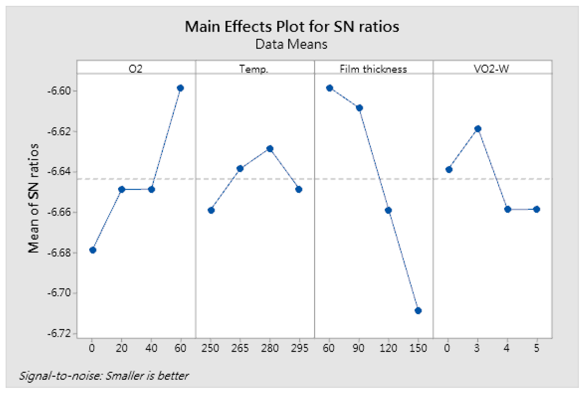
| Response Table for Signal-to-Noise Ratios | ||||
|---|---|---|---|---|
| Level | O2 Flow Rate (sccm) | Substrate Temperature (°C) | Film Thickness (nm) | W Doping Ratio (%) |
| 1 | −6.679 | −6.659 | * −6.598 | −6.639 |
| 2 | −6.649 | −6.639 | −6.608 | * −6.618 |
| 3 | −6.649 | * −6.628 | −6.659 | −6.659 |
| 4 | * −6.598 | −6.648 | −6.709 | −6.659 |
| Delta | 0.081 | 0.031 | 0.111 | 0.040 |
| Rank | 2 | 4 | 1 | 3 |
| Response Table for Signal-to-Noise Ratios | ||||
|---|---|---|---|---|
| Level | O2 Flow Rate (sccm) | Substrate Temperature (°C) | Film Thickness (nm) | VO2-W Ratio (%) |
| 1 | 13.26 | 13.36 | 13.17 | 13.12 |
| 2 | * 13.57 | * 13.53 | 13.19 | 13.49 |
| 3 | 13.22 | 13.37 | * 13.76 | 12.83 |
| 4 | 13.17 | 12.95 | 13.11 | * 13.78 |
| Delta | 0.40 | 0.58 | 0.65 | 0.96 |
| Rank | 4 | 3 | 2 | 1 |
| Response Table for Signal-to-Noise Ratios | ||||
|---|---|---|---|---|
| Level | O2 Flow Rate (sccm) | Substrate Temperature (°C) | Film Thickness (nm) | VO2-W Ratio (%) |
| 1 | * 34.55 | 34.13 | * 35.28 | 33.12 |
| 2 | 32.97 | 33.70 | 35.23 | 33.40 |
| 3 | 34.04 | * 34.21 | 32.85 | 34.25 |
| 4 | 33.91 | 33.42 | 32.11 | * 34.69 |
| Delta | 1.58 | 0.79 | 3.17 | 1.56 |
| Rank | 2 | 4 | 1 | 3 |
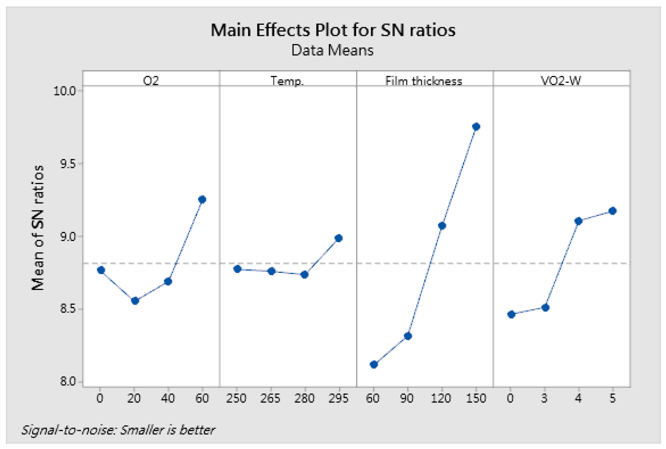
| Response Table for Signal-to-Noise Ratios | ||||
|---|---|---|---|---|
| Level | O2 Flow Rate (sccm) | Substrate Temperature (°C) | Film Thickness (nm) | VO2-W Ratio (%) |
| 1 | 8.765 | 8.774 | 8.113 | 8.465 |
| 2 | 8.554 | 8.761 | 8.316 | 8.513 |
| 3 | 8.691 | 8.737 | 9.074 | 9.109 |
| 4 | * 9.252 | * 8.990 | * 9.759 | * 9.175 |
| Delta | 0.698 | 0.253 | 1.646 | 0.709 |
| Rank | 3 | 4 | 1 | 2 |
| Coating Technique | Visible Light Transmittance | Infrared Transmittance | References |
|---|---|---|---|
| Sol–gel spin coating | 35% | NA | [41] |
| Thermal oxidation | 40–50% | 57% | [42] |
| Spin coating | 35% | NA | [43] |
| DC-reactive magnetron sputtering | 54% | 59% | [44] |
| Pulsed laser deposition | 62.2% | NA | [45] |
| Electron beam evaporation with IAD | 64.33% | 31.34% | This work |
Disclaimer/Publisher’s Note: The statements, opinions and data contained in all publications are solely those of the individual author(s) and contributor(s) and not of MDPI and/or the editor(s). MDPI and/or the editor(s) disclaim responsibility for any injury to people or property resulting from any ideas, methods, instructions or products referred to in the content. |
© 2024 by the authors. Licensee MDPI, Basel, Switzerland. This article is an open access article distributed under the terms and conditions of the Creative Commons Attribution (CC BY) license (https://creativecommons.org/licenses/by/4.0/).
Share and Cite
Tien, C.-L.; Chiang, C.-Y.; Tien, J.-K.; Wang, C.-C.; Lin, S.-C. Surface Characteristics and Performance Optimization of W-Doped Vanadium Dioxide Thin Films. Surfaces 2024, 7, 1109-1124. https://doi.org/10.3390/surfaces7040073
Tien C-L, Chiang C-Y, Tien J-K, Wang C-C, Lin S-C. Surface Characteristics and Performance Optimization of W-Doped Vanadium Dioxide Thin Films. Surfaces. 2024; 7(4):1109-1124. https://doi.org/10.3390/surfaces7040073
Chicago/Turabian StyleTien, Chuen-Lin, Chun-Yu Chiang, Jia-Kai Tien, Ching-Chiun Wang, and Shih-Chin Lin. 2024. "Surface Characteristics and Performance Optimization of W-Doped Vanadium Dioxide Thin Films" Surfaces 7, no. 4: 1109-1124. https://doi.org/10.3390/surfaces7040073
APA StyleTien, C.-L., Chiang, C.-Y., Tien, J.-K., Wang, C.-C., & Lin, S.-C. (2024). Surface Characteristics and Performance Optimization of W-Doped Vanadium Dioxide Thin Films. Surfaces, 7(4), 1109-1124. https://doi.org/10.3390/surfaces7040073