Abstract
Triboelectric nanogenerators (TENGs) based on sliding metal–semiconductor junctions are an emerging technology that can efficiently convert mechanical into electrical energy. These miniature autonomous power sources can output large direct current (DC) densities, but often suffer from limited durability; hence, their practical scope remains uncertain. Herein, through a combination of conductive atomic force microscopy (C-AFM) and photocurrent decay (PCM) experiments, we explored the underlying cause of surface wear during the operation of DC-TENGs. Using monolayer-functionalized Si(211) surfaces as the model system, we demonstrate the extent to which surface damage develops during TENG operation. We reveal that the introduction of surface defects (oxide growth) during TENG operation is not caused by the passage of the rather large current densities (average output of ~2 × 10⁶ A/m2); it is instead mainly caused by the large pressure (~GPa) required for the sliding Schottky diode to output a measurable zero-bias current. We also discovered that the drop in output during operation occurs with a delay in the friction/pressure event, which partially explains why such deterioration of DC-TENG performance is often underestimated or not reported.
1. Introduction
The rapid growth of the Internet of Things and the surging demand for portable electronic devices have fueled the need for autonomous power sources [1,2]. Batteries, while a common and widespread solution to power electronics, are non-regenerative power sources; hence, they need frequent recharging or replacing. Energy harvesting technologies such as piezoelectric nanogenerators (PENGs) and solar cells can convert mechanical and solar energy into electricity but have limitations in terms of cost and need for appropriate illumination [3]. Triboelectric nanogenerators (TENGs) based on contact electrification [4,5] have emerged as a promising power source, offering the means to convert ubiquitous mechanical energy into electrical power [6,7].
The output of a conventional TENG is alternating current [8,9], but recently, there have been a series of breakthroughs towards the development of direct-current (DC) TENGs (DC-TENGs) [10,11,12], which is an important step forward since most microelectronic components rely on DC power. For instance, in 2018, Liu et al. succeeded in showing that friction of an out-of-equilibrium Schottky contact (between Pt and MoS2) can be efficiently converted into DC [13]. This report prompted the search for cheaper and more readily accessible alternatives to MoS2. In this context, silicon represents a promising material for the further development of DC-TENGs [14,15,16].
The mechanism for the mechanic-to-electric energy conversion occurring in a sliding Schottky diode is undoubtedly a surface process dominated by several properties of the metal–semiconductor interface [17]. Consequently, the manipulation of the silicon surface chemistry, for example via hydrosilylation reactions to graft organic monolayers on the surface [18,19], offers a path to maximize TENGs’ performances by controlling wettability, friction, adhesion, and work function [20,21]. Despite the undisputed anodic protection that the attachment of an organic monolayer imparts to the silicon surface when the contact is a (soft) liquid [18,19,22,23], silicon-based Schottky TENGs have so far only shown a limited lifespan, severely restricting their viability [24]. Previous studies have highlighted that the generation of a DC current in Schottky TENGs requires substantial pressure and small contacts [25,26], and that large current densities, up to 109 A/m2, can be obtained [15]. These operational conditions, both the mechanical pressure and localized heating from the flow of a large current density even under zero external bias, can undoubtedly lead to substrate oxidation, hence limiting the durability of Si-based DC-TENGs. Therefore, while minor oxide growth can lead to a temporary enhancement in the DC output [15,27], extensive silicon oxidation results in a complete loss of the triboelectric output [28]. Notably, the passage of current, regardless of the current direction, plays a role in oxide growth [29]. Here, we present a detailed analysis of the underlying causes of surface wear/oxidation during the operation of sliding metal–silicon DC-TENGs. Our study focuses on monolayer-modified Si(211) surfaces, which have demonstrated superior TENG performances in a previous work [28]. We aim to clarify whether surface damage and oxide growth in silicon-based TENGs are primarily caused by pressure and friction or by current-related effects. To address this, we utilized a combination of conductive atomic force microscopy (C-AFM) and photocurrent decay (PCM) experiments. We begin by discussing the characteristics of the model system used in our study, followed by an exploration of the progressive surface damage during sliding events. Subsequently, we present our findings related to surface defects, carrier lifetimes, and current behavior under various conditions. We also discuss the unexpected observations of damaged regions and provide insights into the potential role of flexovoltage. By exploring the progressive surface damage during sliding events and its (detrimental) impact on current generation, we aim to clarify the actual durability of silicon-based TENGs.
2. Materials and Methods
2.1. Chemicals and Materials
Ammonium fluoride (semiconductor grade, 40 wt%, Honeywell, Melbourne, Australia), hydrogen peroxide (MOS Puranal™, 30 wt% in water, Honeywell, Melbourne, Australia), sulfuric acid (VLSI Puranal™, 95–97%, Honeywell, Melbourne, Australia), and Milli-Q water (>18 MΩ cm) were used for sample etching and cleaning procedures. 1,8-Nonadiyne (98%, 1), sodium ascorbate (98%), and methanol (MeOH; HPLC grade, >99.9%) were obtained from Sigma-Aldrich (Castle Hill, Australia) and used without further purification. Si(211) wafers (±0.05, prime grade) were purchased from Siltronix, S.A.S (Archamps, France). Wafers were 500 μm thick, one side polished and N-type (phosphorus-doped), with a resistivity of 7–13 Ω cm. Gallium–indium (Galn) eutectic (99.99%, Sigma-Aldrich, Castle Hill, Australia)) was used to establish an electrical contact between the non-polished side (back side) of the silicon sample and the AFM sample holder.
2.2. Surface Modification Procedures
Silicon wafers were cut into wafers of approximately 1 × 1 cm. Samples were first rinsed with dichloromethane (3 × 50 mL), 2-propanol (3 × 50 mL), and Milli-Q water (5 × 50 mL) and subsequently immersed for 30 min in a hot piranha solution (100 °C, consisting in a 3:1 v/v mixture of concentrated sulfuric acid and 30% hydrogen peroxide). After the piranha bath, samples were rinsed with water (3 × 50 mL) and etched for 13 min in a mixture of deoxygenated ammonium fluoride solution (22.5 mL) and methanol (1 mL) while shielded from ambient light, following reported procedures [28]. Ammonium sulfite was added as oxygen scavenger to the etching mixture and the etching bath was degassed with bubbling argon gas for 15 min before adding the silicon sample. During the etching (13 min), the polished side of the silicon sample was faced upwards. After the etching, the silicon samples were rinsed with water (1 × 50 mL) and dichloromethane (2 × 50 mL), and then covered with a deoxygenated sample of 1. The silicon–hydride diyne-coated samples were then placed inside a UV chamber (312 nm UV source, Vilber, VL-215. M, nominal power output of 30 W) and held for 2 h approximately 20 cm from the UV source. The hydrosilylated product (the S-1 surface, Figure 1a) was rinsed with dichloromethane (1 × 50 mL) and stored overnight at +4 °C under dichloromethane in a sealed sample tube prior to analysis.
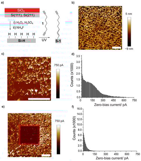
Figure 1.
(a) Chemical strategy used for the cleaning, etching, and passivation of silicon samples. Hydrogen-terminated Si(211) samples were reacted under a UV-assisted hydrosilylation reaction with dyine 1 to yield the covalent, monolayer-modified S-1 surface. (b) AFM topography image (5 × 5 µm scan size) of a Si(211) S-1 sample. (c) Zero-voltage bias C-AFM map of S-1 sample obtained in a 2 × 2 µm region. The applied normal load was 360 nN, and the contact area (Pt–Si contact) was estimated to be ~80 nm2; hence, the normal pressure was ~4.5 GPa. (d) Current distribution histogram plot obtained from the C-AFM map shown in panel (c). (e) Wide zero-voltage bias C-AFM map (5 × 5 µm) of a S-1 sample. The area marked by a red square is the region where the C-AFM scan of panel (c) was performed. (f) Current histogram for the C-AFM map (area marked by a red square only) of panel (e). The histogram counts refer to the number of pixels (sample locations) of a given current value/bin, with a total of ∼65 K pixels making up an entire C-AFM map (5 × 5 µm). The horizontal scale bars in panels (b,c,e) indicate 1 μm.
2.3. Atomic Force Microscopy Characterization
Atomic force microscopy (AFM) topography maps, zero-bias current maps, and lateral force (friction) scans were performed using a NX10 microscope (Park Systems Corporation, Suwon, Korea). Measurements were performed using a single solid platinum tip (25PT300B, Rocky Mountain Nanotechnology, Holladay, Utah) with a nominal resonance frequency of 14 kHz, a spring constant of 18 N/m, and a tip radius of ∼20 nm; set points were either 50 or 360 nN. The silicon samples–Pt tip contact area was estimated against the Derjaguin, Muller, and Toporov (DMT) model (described in the Supplementary Materials) [30]. The imaging resolution was set to 256 points/line and the scan rate to 1 Hz, and scan size ranged from 2 × 2 µm to 5 × 5 µm. Reverse currents have a positive sign and are indicative of an electron flow from the Pt tip to the silicon sample. The maximum zero-bias current output was taken as the output of the 99th percentile [31]. The vertical height and current scale bars (color-coded) for the AFM measurements do not cover the full scale. The color range was arbitrarily set to maximize the visual clarity of topographic and current features. The instrument current noise was around ∼120 fA. AFM data were processed with the XEI software (version 4.3, Park Systems). Transient photocurrent measurements (PCM) were recorded at 10 separate sample locations; the laser wavelength was 635 nm and the nominal laser power output was 5 mW. Current transients decay curves were fitted using Origin 9.0™ software. Statistical analysis was performed in Python. Ohmic contact between the AFM stage and the silicon samples was ensured by applying a small amount of GaIn eutectic to the non-polished silicon side and gently rubbing it with sandpaper. Samples were further secured in the AFM stage with conductive copper tape. All measurements were conducted in air at ambient temperature (24 ± 2 °C).
3. Results and Discussion
Our research focuses on Si(211) crystals, a choice based on the fact that the surface conductivity of Si(211) is greater than that of both Si(100) and Si(111) [32,33]. This makes Si(211) an excellent candidate for DC-TENGs. The native oxide first needs to be removed to ensure sufficient electrical conductivity, and the resulting (hydride) surface needs to be chemically passivated to allow handling the samples under ambient air without significant oxidation. To this end, Si–C-bound monolayers of 1,8-nonadiyne, 1, were prepared following published procedures (Figure 1a) [19,34,35]. Silicon oxide samples were first etched to expose a Si–H surface, which is reactive towards 1-alkynes such as the α,ω-dialkyne molecule 1. This chemical strategy (S-1) prevents spontaneous semiconductor oxidation and enhances the generation of a DC output in response to mechanical stimuli such as vibrations and friction [20].
Wet-etched Si(211) has a rougher surface compared to other Si crystal cuts, such as, for example, Si(111) and Si(100) [28,34]. Figure 1b shows an AFM topography map of a Si(211) S-1 sample, with evident rounded features, and a root-mean-square (RMS) roughness of ~3 nm, a value comparable to those of published results [28], and which is at present the smoother Si(211) surface achievable via wet chemistry methods. We then acquired a zero-bias current (C-AFM) map (2 × 2 µm) to measure the current generation upon lateral movement of the solid platinum AFM tip across the semiconductor surface (Figure 1c). Figure 1d shows the DC distribution for the map in Figure 1c and reveals that the current ranged from noise level up to 750 pA. The average output was ~120 pA, and 1% of the sampled points returned current values above 700 pA. The average current density was in the order of ~2 × 10⁶ A/m2.
This tribocurrent was measured under zero external bias, and it bears the sign of a reverse current, that is, electrons flowing from the Pt tip to the silicon surface. Notably, in our C-AFM experiments, the pressure reached a pressure of ~4.5 GPa. To evaluate the surface damage, if any, induced after the initial current map scan (2 × 2 µm), we repeated the C-AFM measurement expanding the scan area to a 5 × 5 µm region (Figure 1e). Interestingly, the surface area previously scanned (region marked by a red square in Figure 1e) returned a significantly reduced current output. The average current dropped to ~20 pA (current density ~3 × 10⁵ A/m2, Figure 1f). This drop in output is a ~83% reduction in current density within the scanned area, which highlights the propensity of DC-TENGs to rapid wear. Similar current attenuations have been previously reported in AFM experiments on silicon surfaces under an external bias and were linked to oxide growth [29]. We then tested the system under a lower normal force set point (~50 nN) to verify whether this may increase device longevity (Figure S1, Supplementary Materials). As expected, C-AFM data obtained under a smaller normal force indicate a less pronounced loss of performance during operation, but unfortunately, this comes at the cost of a significantly lower tribocurrent output.
It is technically hard to acquire XPS spectra to verify the presence of oxide inside a 2 × 2 µm region; hence, we opted for a spatially resolved measurement of surface defects rather than direct spectroscopic evidence of silicon oxidation. We conducted spatially and time-resolved photoconductivity (PCM) experiments to evaluate the recombination velocities of charge carriers, trying to assess the introduction of surface defects during TENG operation. Figure 2a depicts a PCM measurement, and Figure 2b displays representative transient photocurrent decay traces for static Pt–S-1 junctions, inside and outside the putatively oxidized square (Figure 2c).
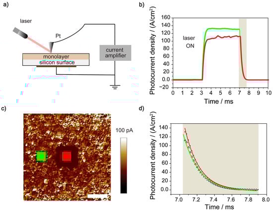
Figure 2.
Spatially and time-resolved photoconductivity (PCM) measurements (AFM-based) conducted on S-1 surfaces. (a) Schematic representation of the PCM measurement performed to calculate the carrier lifetime from the transient photocurrent response. (b) Representative PCM traces on S-1 surfaces. The shaded grey colored area indicates the region of the curve where the exponential fit was conducted. (c) C-AFM map of a S-1 sample conducted at zero-voltage bias in a 5 × 5 µm area after a previous scan conducted in a 1 × 1 µm scan area (center of the image). The horizontal scale bar in panel (c) indicates 1 μm. (d) Exponential fits to the photocurrent curves sampled inside and outside the square shown in panel (c).
Unfortunately, a stable and strong photocurrent response is not always present, and approximately half of the sampled locations did not return traces like those in Figure 2b; rather, they resembled those shown in Figure S2 (Supplementary Materials). The “non-ideal” transients shown in Figure S1 are characterized by a capacitive charging/discharging behavior and could not be used to extract information on recombination velocities. The fitting of more ideal photoconductive locations (Figure 2d) returned significantly different carrier lifetimes inside versus outside the square. The average carrier’s lifetime inside the square was 147.9 ± 10.7 µs (the uncertainty is the 99% confidence limit of the mean; the lower and upper bound were 137.2 µs and 158.6 µs, respectively). The average carrier’s lifetime outside the square was 188.1 ± 15.7 (lower and upper bound of 172.4 µs and 203.8 µs, respectively). The confidence limit was calculated as tn−1s/n1/2, where tn−1 is 3.01 for 10 different samples, n is the number of measurements, and s is the standard deviation [31]. In summary, sample locations within the initially scanned area returned a higher surface recombination velocity (i.e., lower time constant), which suggests the introduction of electronic defects, most likely linked to the onset of substrate oxidation, during TENG operations.
The reason such a drastic drop in TENG performance is often unnoticed is perhaps because it is customary to screen for such current changes by comparing outputs of sequential trace and retrace scans. This point warrants further explanation. A conventional C-AFM measurement, as for those shown in Figure 3a and Figure S3 (Supplementary Materials), allows one to simultaneously measure current and map topography (Figure 3b). The sliding Pt tip scans the same topographical feature, sequentially, in both the trace and retrace directions. What is indeed very surprising is that the oxidative damage and corresponding drop in TENG output discussed above (Figure 1 and Figure 2) for microscopic regions has no parallel drop in current output when one tries specifically detect this based on a single line of trace/retrace measurement (Figure 3c,d). In fact, retrace currents can even reach slightly higher DC outputs than those for trace scans (Figure 3b).
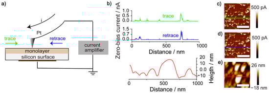
Figure 3.
(a) Schematic representation of the C-AFM measurement; the platinum tip is sliding in both trace and retrace directions, through a silicon (S-1) sample. (b) Zero-bias DC current and topography profiles obtained during C-AFM experiments. The green and blue color coding indicates the direction of the scan: first a trace (green, left to right) and then a retrace (blue, right to left) over the same line. The topographic (height) profile is indicated by the red trace. (c–e) C-AFM and topography maps indicating the location of the line along which the current trace (green), current retrace (blue), and topography (red) data of panel (b) were acquired.
The data in Figure 3 show just this, as well as showing that the zero-bias current peaks at concave locations on the Si(211) surface. This effect has been previously reported by Ferrie et al. for Si(111)/(100) pyramids generated via the anisotropic etching of Si(100) substrates with potassium hydroxide solutions [14]. The same authors also did not observe oxidative damage when conducting trace/retrace scans and stressed that tribocurrent discharging happened at the base of the pyramid rather than at its apex. This was explained tentatively as consequence of the space charge region becoming thinner at concave sites [36].
Furthermore, it did not escape our attention that the AFM tip is twisting (based on lateral deflection data) at the edge of the protrusions (Figure S4, Supplementary Materials). This point will require further investigation and the electronic component of friction remains debated [37]. Recently, Marks and co-workers have suggested that flexoelectricity (i.e., linear coupling between strain gradients and voltage) is the “missing term” in the contact electrification process [38]. We therefore suggest that flexovoltage generated during or immediately after tip twisting may be responsible for the peaking of the current near the protrusions, shown in Figure 3. Whether or not reduction in the thickness of the space charge layer at concave sites and flexoelectric effects are linked remains to be explored [39,40].
Finally, in order to separate the impact of friction/pressure on surface damage from damage caused by the very-high-current densities of a DC-TENG, we conducted C-AFM experiments with an external DC bias of such magnitude and direction to nullify the flow of the current, while making sure not to introduce changes to the normal load and friction of the sliding platinum tip (Figure 4a). Results depicted in Figure 4b,c indicate that the drop in DC-TENG output is not caused by the passage of a tribocurrent, again reinforcing the above conclusions that substrate oxidation in response to pressure and friction is the main cause of output loss. A further note, which may stimulate future investigations, is that we very often observed large tribocurrents near the edge of previously oxidized regions (Figure 4b,c). The reason for such (localized) enhancement of DC output is at present unclear.
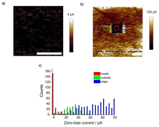
Figure 4.
(a) Nullifying-bias DC current output C-AFM experiments with a current reading close to noise level. (b) C-AFM current map obtained at zero-bias scan in a 2 × 2 µm area after the experiment of panel (a). In the study, a load of 360 nN was applied to the sample, and the estimated contact area was on the order of 80 nm2. (c) Current distribution histogram plot obtained from the C-AFM map; the yellow square corresponds to the C-AFM scan conducted at nullifying voltage, the green square corresponds to tribospots outside the square, and the blue square corresponds to tribospots close to the edge of the square. On the histograms, the counts indicate the number of pixels (sample locations) of a given current, with a total of ∼65 K pixels making up a C-AFM map. The horizontal scale bars in parts a and b are 1 μm.
4. Conclusions
We quantified the extent of operational damage for DC-TENGs based on sliding Si(211)–organic monolayer–platinum Schottky diodes and attempted to define the relative importance of friction-/pressure-induced wear versus oxidative damages to the semiconductor due to the flow of the large current densities (~2 × 10⁶ A/m2) reached during the operation of these miniature autonomous power sources. Using conductive atomic force microscopy (C-AFM) experiments and photocurrent decay measurements (PCM), we revealed that oxide growth and loss of TENG performances upon operation are not primarily caused by the passage of the current, but are rather more strictly linked to pressure- and friction-induced surface wear. Results revealed that current density drops from ~2 × 10⁶ A/m2 to ~3 × 10⁵ A/m2, representing a current decay of ~83%. The carrier lifetime within damaged regions was found to be 147.9 ± 10.7 µs, compared to 188.1 ± 15.7 µs outside damaged areas, emphasizing the impact of surface defects on charge recombination. We also present evidence of a time delay between the friction/pressure event and the manifestation of the surface damage (drop in TENG output). Further, a note which we believe will stimulate future studies: (i) zero-bias DC outputs are significantly higher at the edge of damaged areas, an observation for which we currently lack an explanation, and (ii) outputs are generally greater at concave semiconductor locations, which may be the result of a localized thinning of the space charge layer (i.e., enhanced flexoelectric effect).
Supplementary Materials
The following supporting information can be downloaded at: https://www.mdpi.com/article/10.3390/surfaces6030020/s1, Figures S1–S4, and description of the methodology for contact area (Pt AFM tip–S1 sample) determination.
Author Contributions
Conceptualization, C.H. and S.C.; methodology, C.H and S.C.; software, C.H.; validation, C.H. and S.C.; formal analysis, C.H. and S.C.; investigation, C.H.; resources, S.C.; data curation, C.H.; writing—original draft preparation, C.H.; writing—review and editing, S.C.; visualization, C.H.; supervision, S.C.; project administration, S.C.; funding acquisition, S.C. All authors have read and agreed to the published version of the manuscript.
Funding
This research was funded by the Australian Research Council (Grants DP220100735 and FT190100148).
Informed Consent Statement
Not applicable.
Data Availability Statement
The data presented in this study are available on request from the corresponding author.
Conflicts of Interest
The authors declare no conflict of interest.
References
- Xiang, S.; Wang, Y.; Zhang, C.; Zhao, Z.; Wang, B.; Zou, W.; Wu, J. Smart Contact Lenses for the New Era of IoT: Integrated Biosensors, Circuits, and Human–Machine Interface Systems. Adv. Mater. Technol. 2023, 8, 2201185. [Google Scholar] [CrossRef]
- Le, X.; Guo, X.; Lee, C. Evolution of Micro-Nano Energy Harvesting Technology—Scavenging Energy from Diverse Sources towards Self-Sustained Micro/Nano Systems. Nanoenergy Adv. 2023, 3, 101–125. [Google Scholar] [CrossRef]
- Mariello, M.; Guido, F.; Mastronardi, V.M.; Todaro, M.T.; Desmaële, D.; De Vittorio, M. Nanogenerators for harvesting mechanical energy conveyed by liquids. Nano Energy 2019, 57, 141–156. [Google Scholar] [CrossRef]
- Zheng, M.; Lin, S.; Xu, L.; Zhu, L.; Wang, Z.L. Scanning Probing of the Tribovoltaic Effect at the Sliding Interface of Two Semiconductors. Adv. Mater. 2020, 32, e2000928. [Google Scholar] [CrossRef]
- Lin, S.; Lin Wang, Z. The tribovoltaic effect. Mater. Today 2023, 62, 111–128. [Google Scholar] [CrossRef]
- Song, Y.; Wang, N.; Wang, Y.; Zhang, R.; Olin, H.; Yang, Y. Direct Current Triboelectric Nanogenerators. Adv. Energy Mater. 2020, 10, 2002756. [Google Scholar] [CrossRef]
- Wu, C.; Wang, A.C.; Ding, W.; Guo, H.; Wang, Z.L. Triboelectric Nanogenerator: A Foundation of the Energy for the New Era. Adv. Energy Mater. 2019, 9, 1802906. [Google Scholar] [CrossRef]
- Seol, M.-L.; Woo, J.-H.; Jeon, S.-B.; Kim, D.; Park, S.-J.; Hur, J.; Choi, Y.-K. Vertically stacked thin triboelectric nanogenerator for wind energy harvesting. Nano Energy 2015, 14, 201–208. [Google Scholar] [CrossRef]
- Wang, Z.L. Triboelectric nanogenerator (TENG)—Sparking an energy and sensor revolution. Adv. Energy Mater. 2020, 10, 2000137. [Google Scholar] [CrossRef]
- Liu, D.; Zhou, L.; Wang, Z.L.; Wang, J. Triboelectric nanogenerator: From alternating current to direct current. iScience 2021, 24, 102018. [Google Scholar] [CrossRef]
- You, Z.; Wang, S.; Li, Z.; Zou, Y.; Lu, T.; Wang, F.; Hu, B.; Wang, X.; Li, L.; Fang, W.; et al. High current output direct-current triboelectric nanogenerator based on organic semiconductor heterojunction. Nano Energy 2022, 91, 106667. [Google Scholar] [CrossRef]
- Naval, S.; Jain, A.; Mallick, D. Direct current triboelectric nanogenerators: A review. J. Micromech. Microeng. 2022, 33, 013001. [Google Scholar] [CrossRef]
- Liu, J.; Goswami, A.; Jiang, K.; Khan, F.; Kim, S.; McGee, R.; Li, Z.; Hu, Z.; Lee, J.; Thundat, T. Direct-current triboelectricity generation by a sliding Schottky nanocontact on MoS2 multilayers. Nat. Nanotechnol. 2018, 13, 112–116. [Google Scholar] [CrossRef] [PubMed]
- Ferrie, S.; Darwish, N.; Gooding, J.J.; Ciampi, S. Harnessing silicon facet-dependent conductivity to enhance the direct-current produced by a sliding Schottky diode triboelectric nanogenerator. Nano Energy 2020, 78, 105210. [Google Scholar] [CrossRef]
- Lyu, X.; Ferrie, S.; Pivrikas, A.; MacGregor, M.; Ciampi, S. Sliding Schottky diode triboelectric nanogenerators with current output of 109 A/m2 by molecular engineering of Si (211) surfaces. Nano Energy 2022, 102, 107658. [Google Scholar] [CrossRef]
- Lyu, X.; MacGregor, M.; Liu, J.; Darwish, N.; Ciampi, S. Direct-current output of silicon–organic monolayer–platinum Schottky TENGs: Elusive friction-output relationship. Nano Energy 2023, 114, 108627. [Google Scholar] [CrossRef]
- Liu, J.; Ciampi, S.; Antony, A. The Origins of Solid-Solid Contact Electrification. In Handbook of Triboelectric Nanogenerators; Wang, Z.L., Yang, Y., Zhai, J., Wang, J., Eds.; Springer International Publishing: Cham, Switzerland, 2023; pp. 1–37. [Google Scholar]
- Fabre, B. Functionalization of Oxide-Free Silicon Surfaces with Redox-Active Assemblies. Chem. Rev. 2016, 116, 4808–4849. [Google Scholar] [CrossRef]
- Ciampi, S.; Harper, J.B.; Gooding, J.J. Wet chemical routes to the assembly of organic monolayers on silicon surfaces via the formation of Si-C bonds: Surface preparation, passivation and functionalization. Chem. Soc. Rev. 2010, 39, 2158–2183. [Google Scholar] [CrossRef]
- Ferrie, S.; Le Brun, A.P.; Krishnan, G.; Andersson, G.G.; Darwish, N.; Ciampi, S. Sliding silicon-based Schottky diodes: Maximizing triboelectricity with surface chemistry. Nano Energy 2022, 93, 106861. [Google Scholar] [CrossRef]
- Lyu, X.; Ciampi, S. Improving the performances of direct-current triboelectric nanogenerators with surface chemistry. Curr. Opin. Colloid Interface Sci. 2022, 61, 101627. [Google Scholar] [CrossRef]
- Fabre, B. Ferrocene-Terminated Monolayers Covalently Bound to Hydrogen-Terminated Silicon Surfaces. Toward the Development of Charge Storage and Communication Devices. Acc. Chem. Res. 2010, 43, 1509–1518. [Google Scholar] [CrossRef] [PubMed]
- Vogel, Y.B.; Zhang, L.; Darwish, N.; Gonçales, V.R.; Le Brun, A.; Gooding, J.J.; Molina, A.; Wallace, G.G.; Coote, M.L.; Gonzalez, J.; et al. Reproducible flaws unveil electrostatic aspects of semiconductor electrochemistry. Nat. Commun. 2017, 8, 2066. [Google Scholar] [CrossRef] [PubMed]
- Deng, S.; Xu, R.; Seh, W.; Sun, J.; Cai, W.; Zou, J.; Zhang, Q. Current degradation mechanism of tip contact metal-silicon Schottky nanogenerator. Nano Energy 2022, 94, 106888. [Google Scholar] [CrossRef]
- Park, S.M.; Wang, B.; Chen, L.-Q.; Noh, T.W.; Yang, S.M.; Lee, D. Flexoelectric control of physical properties by atomic force microscopy. Appl. Phys. Rev. 2021, 8, 041327. [Google Scholar] [CrossRef]
- Qiao, H.; Zhao, P.; Kwon, O.; Sohn, A.; Zhuo, F.; Lee, D.M.; Sun, C.; Seol, D.; Lee, D.; Kim, S.W. Mixed triboelectric and flexoelectric charge transfer at the nanoscale. Adv. Sci 2021, 8, 2101793. [Google Scholar] [CrossRef]
- Uritsky, V. Role of Electron/Hole Processes in the Initial Stage of Silicon Anodization; Materials Science Forum, Trans Tech Publications: Baech, Switzerland, 1995; pp. 115–118. [Google Scholar]
- Hurtado, C.; Lyu, X.; Ferrie, S.; Le Brun, A.P.; MacGregor, M.; Ciampi, S. Organic Monolayers on Si(211) for Triboelectricity Generation: Etching Optimization and Relationship between the Electrochemistry and Current Output. ACS Appl. Nano Mater. 2022, 5, 14263–14274. [Google Scholar] [CrossRef]
- Peiris, C.R.; Ferrie, S.; Ciampi, S.; Rickard, W.D.A.; Darwish, N. Memristor Arrays Formed by Reversible Formation and Breakdown of Nanoscale Silica Layers on Si–H Surfaces. ACS Appl. Nano Mater. 2022, 5, 6609–6617. [Google Scholar] [CrossRef]
- Park, J.Y.; Salmeron, M. Fundamental Aspects of Energy Dissipation in Friction. Chem. Rev. 2014, 114, 677–711. [Google Scholar] [CrossRef]
- Miller, J.N.; Miller, J.C.; Miller, R.D. Statistics and Chemometrics for Analytical Chemistry, 7th ed.; Pearson Education Limited: Harlow, UK, 2018. [Google Scholar]
- Zhang, S.; Ferrie, S.; Lyu, X.; Xia, Y.; Darwish, N.; Wang, Z.; Ciampi, S. Absence of a Relationship between Surface Conductivity and Electrochemical Rates: Redox-Active Monolayers on Si(211), Si(111), and Si(110). J. Phys. Chem. C 2021, 125, 18197–18203. [Google Scholar] [CrossRef]
- Tan, C.S.; Hsieh, P.L.; Chen, L.J.; Huang, M.H. Silicon Wafers with Facet-Dependent Electrical Conductivity Properties. Angew. Chem. Int. Ed. 2017, 129, 15541–15545. [Google Scholar] [CrossRef]
- Ciampi, S.; Böcking, T.; Kilian, K.A.; James, M.; Harper, J.B.; Gooding, J.J. Functionalization of Acetylene-Terminated Monolayers on Si(100) Surfaces: A Click Chemistry Approach. Langmuir 2007, 23, 9320–9329. [Google Scholar] [CrossRef] [PubMed]
- Ng, A.; Ciampi, S.; James, M.; Harper, J.B.; Gooding, J.J. Comparing the reactivity of alkynes and alkenes on silicon (100) surfaces. Langmuir 2009, 25, 13934–13941. [Google Scholar] [CrossRef] [PubMed]
- Zhang, X. Mechanism of pore formation on n-type silicon. J. Electrochem. Soc. 1991, 138, 3750. [Google Scholar] [CrossRef]
- Park, J.Y.; Ogletree, D.F.; Thiel, P.A.; Salmeron, M. Electronic Control of Friction in Silicon pn Junctions. Science 2006, 313, 186. [Google Scholar] [CrossRef]
- Mizzi, C.A.; Lin, A.Y.W.; Marks, L.D. Does flexoelectricity drive triboelectricity? Phys. Rev. Lett. 2019, 123, 1. [Google Scholar] [CrossRef]
- Zhang, X.G.; Collins, S.D.; Smith, R.L. Porous silicon formation and electropolishing of silicon by anodic polarization in HF solution. J. Electrochem. Soc. 1989, 136, 1561–1565. [Google Scholar] [CrossRef]
- Olson, K.P.; Mizzi, C.A.; Marks, L.D. Band Bending and Ratcheting Explain Triboelectricity in a Flexoelectric Contact Diode. Nano Lett. 2022, 22, 3914–3921. [Google Scholar] [CrossRef]
Disclaimer/Publisher’s Note: The statements, opinions and data contained in all publications are solely those of the individual author(s) and contributor(s) and not of MDPI and/or the editor(s). MDPI and/or the editor(s) disclaim responsibility for any injury to people or property resulting from any ideas, methods, instructions or products referred to in the content. |
© 2023 by the authors. Licensee MDPI, Basel, Switzerland. This article is an open access article distributed under the terms and conditions of the Creative Commons Attribution (CC BY) license (https://creativecommons.org/licenses/by/4.0/).