In Situ Monitoring of Growth of Vertically Stacked h-BN/Graphene Heterostructures on Ni Substrates and Their Interface Interaction


Abstract
:
1. Introduction
2. Experiments
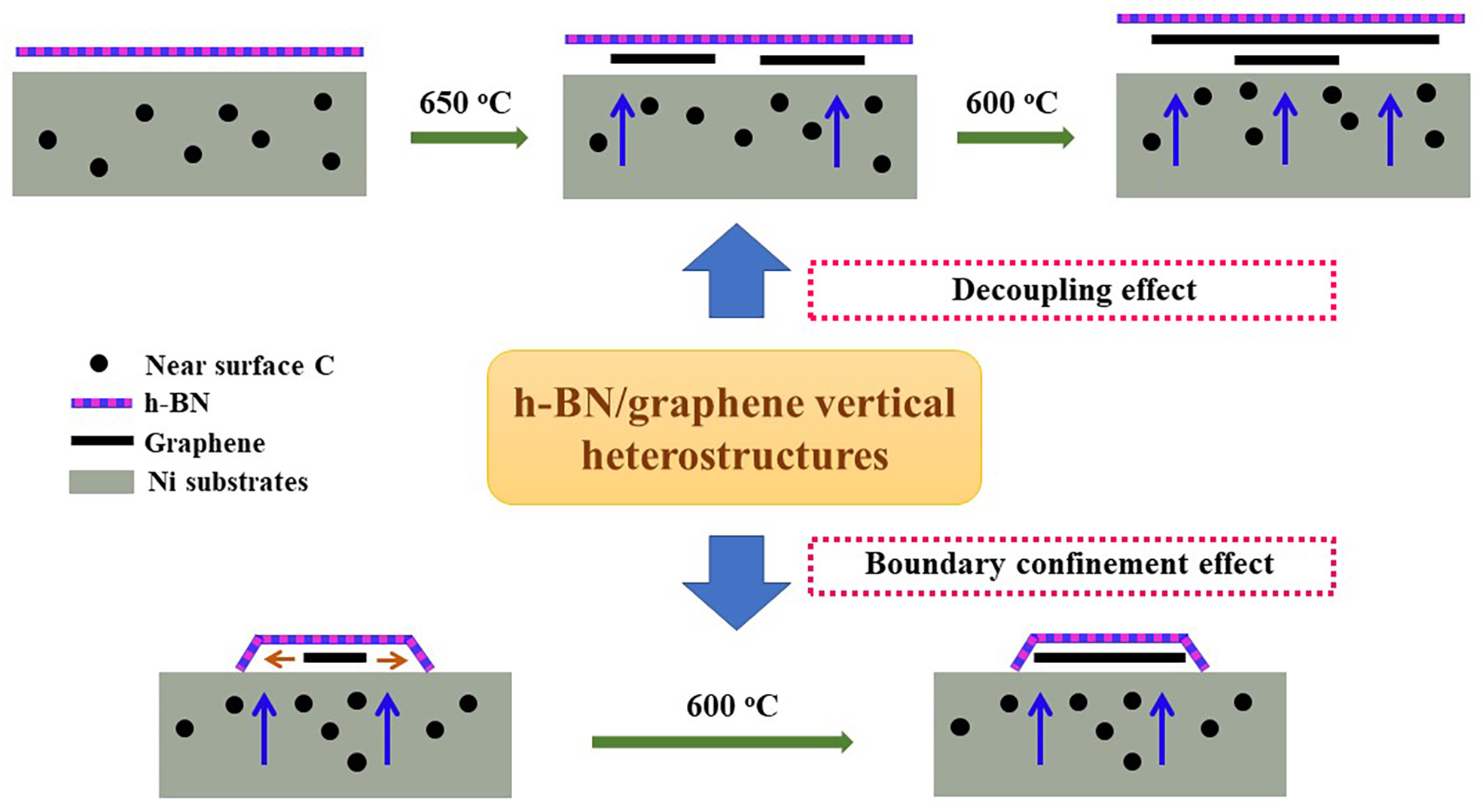
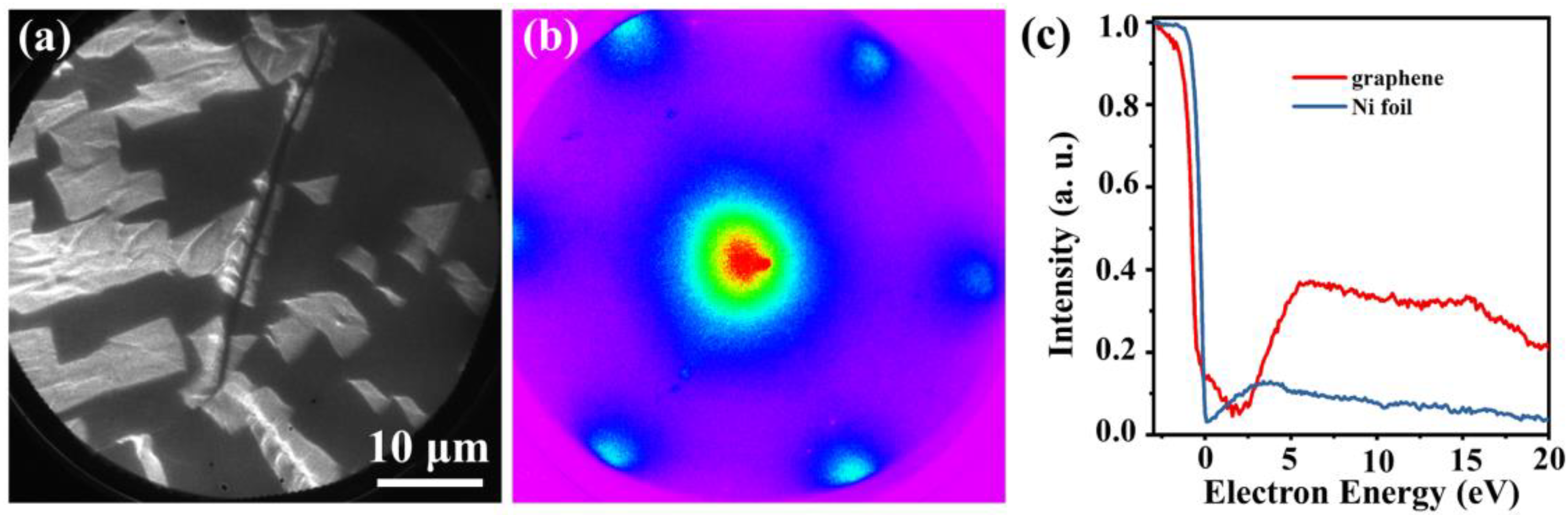
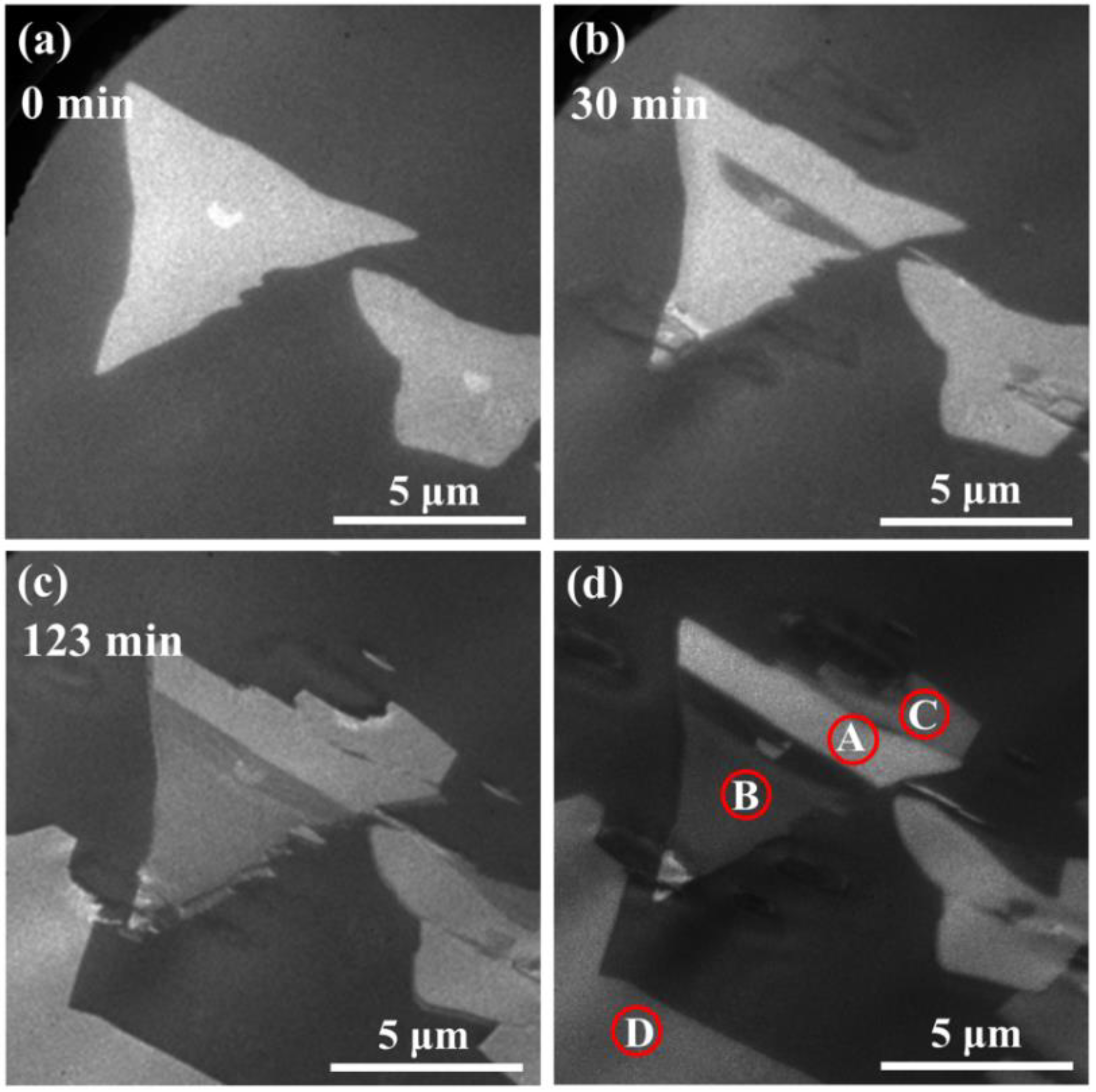
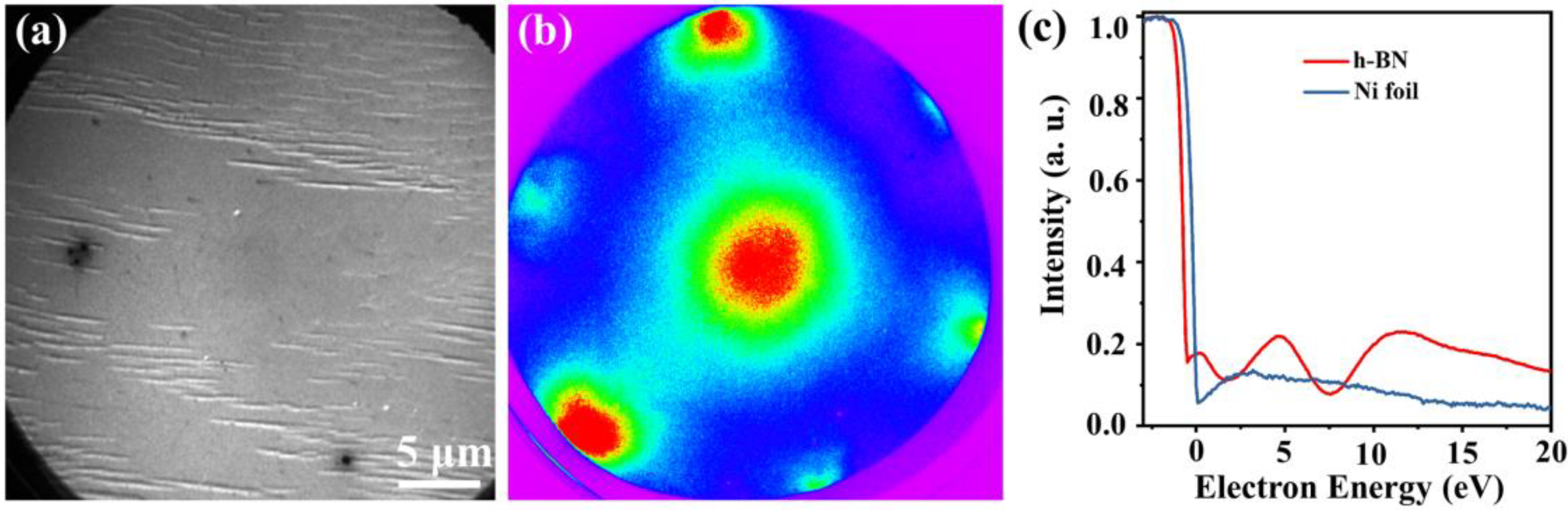
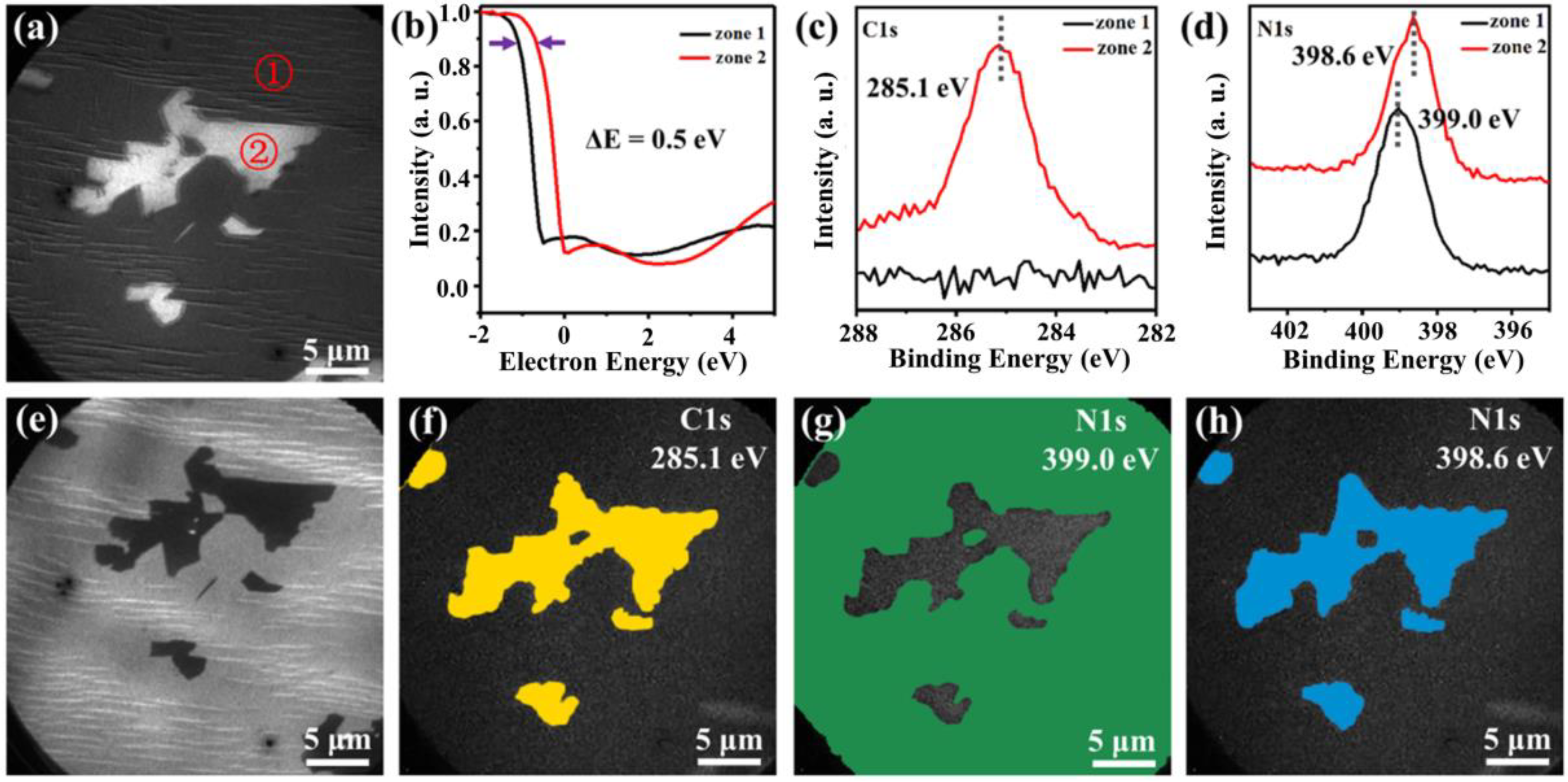
3. Results
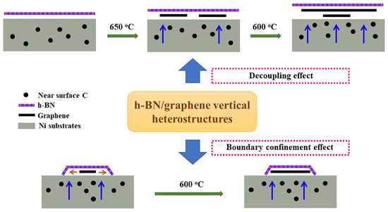
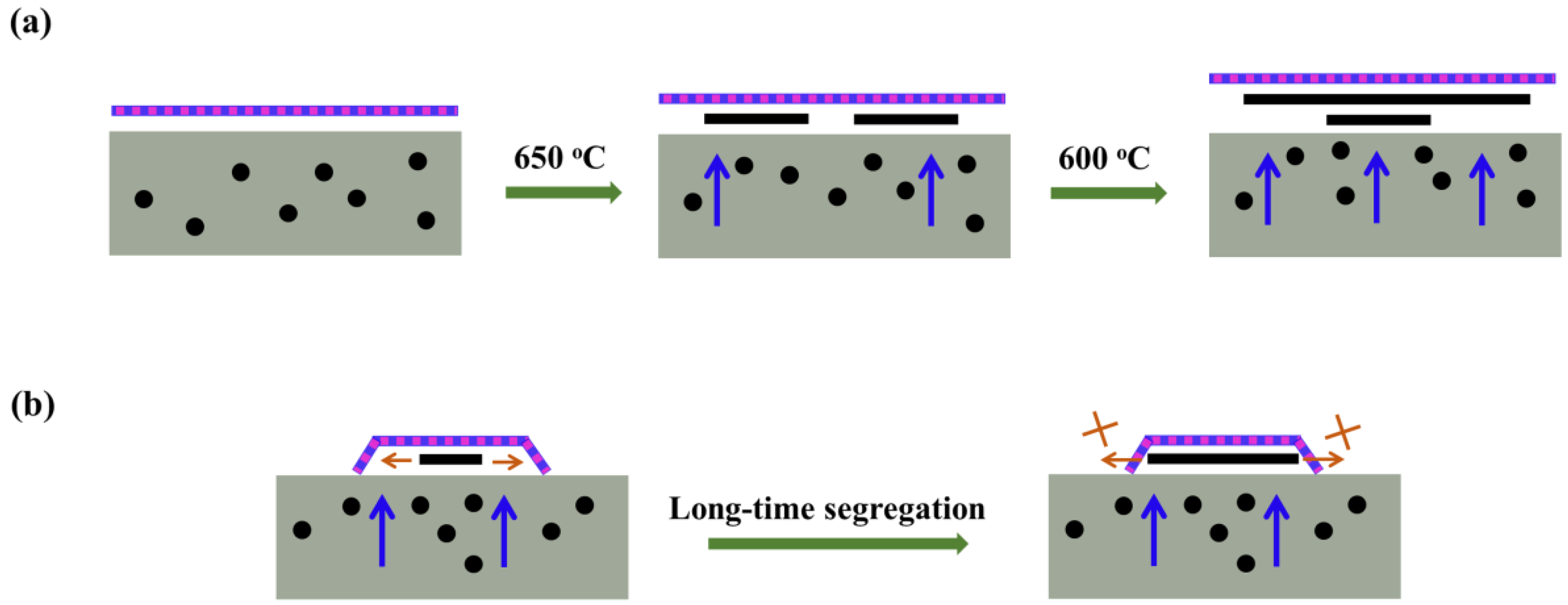
4. Discussion
5. Conclusions
Supplementary Materials
Author Contributions
Funding
Conflicts of Interest
References
- Schwierz, F. Graphene transistors. Nat. Nanotechnol. 2010, 5, 487–496. [Google Scholar] [CrossRef] [PubMed]
- Chen, J.-H.; Ishigami, M.; Jang, C.; Hines, D.R.; Fuhrer, M.S.; Williams, E.D. Printed graphene circuits. Adv. Mater. 2007, 19, 3623. [Google Scholar] [CrossRef] [Green Version]
- Bonaccorso, F.; Sun, Z.; Hasan, T.; Ferrari, A.C. Graphene photonics and optoelectronics. Nat. Photonics 2010, 4, 611–622. [Google Scholar] [CrossRef] [Green Version]
- Stoeberl, U.; Wurstbauer, U.; Wegscheider, W.; Weiss, D.; Eroms, J. Morphology and flexibility of graphene and few-layer graphene on various substrates. Appl. Phys. Lett. 2008, 93, 051906. [Google Scholar] [CrossRef] [Green Version]
- Ishigami, M.; Chen, J.H.; Cullen, W.G.; Fuhrer, M.S.; Williams, E.D. Atomic structure of graphene on SiO2. Nano Lett. 2007, 7, 1643–1648. [Google Scholar] [CrossRef] [PubMed] [Green Version]
- Chen, J.-H.; Jang, C.; Xiao, S.; Ishigami, M.; Fuhrer, M.S. Intrinsic and extrinsic performance limits of graphene devices on SiO2. Nat. Nanotechnol. 2008, 3, 206–209. [Google Scholar] [CrossRef] [PubMed]
- Ando, T. Screening effect and impurity scattering in monolayer graphene. J. Phys. Soc. Jpn. 2006, 75, 074716. [Google Scholar] [CrossRef] [Green Version]
- Kho, J.-G.; Moon, K.-T.; Kim, J.-H.; Kim, D.-P. Properties of boron nitride films produced by the spin-coating process of polyborazine. J. Am. Ceram. Soc. 2000, 83, 2681–2683. [Google Scholar] [CrossRef]
- Kim, K.K.; Hsu, A.; Jia, X.; Kim, S.M.; Shi, Y.; Hofmann, M.; Nezich, D.; Rodriguez-Nieva, J.F.; Dresselhaus, M.; Palacios, T.; et al. Synthesis of monolayer hexagonal boron nitride on Cu foil using chemical vapor deposition. Nano Lett. 2012, 12, 161–166. [Google Scholar] [CrossRef]
- Xue, J.; Sanchez-Yamagishi, J.; Bulmash, D.; Jacquod, P.; Deshpande, A.; Watanabe, K.; Taniguchi, T.; Jarillo-Herrero, P.; Leroy, B.J. Scanning tunnelling microscopy and spectroscopy of ultra-flat graphene on hexagonal boron nitride. Nat. Mater. 2011, 10, 282–285. [Google Scholar] [CrossRef] [Green Version]
- Ling, X.; Fang, W.; Lee, Y.-H.; Araujo, P.T.; Zhang, X.; Rodriguez-Nieva, J.F.; Lin, Y.; Zhang, J.; Kong, J.; Dresselhaus, M.S. Raman enhancement effect on two-dimensional layered materials: Graphene, h-BN and MoS2. Nano Lett. 2014, 14, 3033–3040. [Google Scholar] [CrossRef] [PubMed]
- Liu, Z.; Song, L.; Zhao, S.; Huang, J.; Ma, L.; Zhang, J.; Lou, J.; Ajayan, P.M. Direct growth of graphene/hexagonal boron nitride stacked layers. Nano Lett. 2011, 11, 2032–2037. [Google Scholar] [CrossRef] [PubMed]
- Kim, S.M.; Hsu, A.; Araujo, P.T.; Lee, Y.-H.; Palacios, T.; Dresselhaus, M.; Idrobo, J.-C.; Kim, K.K.; Kong, J. Synthesis of patched or stacked graphene and h-BN flakes: A route to hybrid structure discovery. Nano Lett. 2013, 13, 933–941. [Google Scholar] [CrossRef]
- Song, X.; Gao, T.; Nie, Y.; Zhuang, J.; Sun, J.; Ma, D.; Shi, J.; Lin, Y.; Ding, F.; Zhang, Y.; et al. Seed-assisted growth of single-crystalline patterned graphene domains on hexagonal boron nitride by chemical vapor deposition. Nano Lett. 2016, 16, 6109–6116. [Google Scholar] [CrossRef] [PubMed]
- Yang, Y.; Fu, Q.; Li, H.; Wei, M.; Xiao, J.; Wei, W.; Bao, X. Creating a nanospace under an h-BN cover for adlayer growth on nickel(111). ACS Nano 2015, 9, 11589–11598. [Google Scholar] [CrossRef]
- Li, Q.; Zhao, Z.; Yan, B.; Song, X.; Zhang, Z.; Li, J.; Wu, X.; Bian, Z.; Zou, X.; Zhang, Y.; et al. Nickelocene-precursor-facilitated fast growth of graphene/h-BN vertical heterostructures and its applications in OLEDs. Adv. Mater. 2017, 29, 1701325. [Google Scholar] [CrossRef] [PubMed]
- Yang, W.; Chen, G.; Shi, Z.; Liu, C.-C.; Zhang, L.; Xie, G.; Cheng, M.; Wang, D.; Yang, R.; Shi, D.; et al. Epitaxial growth of single-domain graphene on hexagonal boron nitride. Nat. Mater. 2013, 12, 792. [Google Scholar] [CrossRef]
- Zhang, C.; Zhao, S.; Jin, C.; Koh, A.L.; Zhou, Y.; Xu, W.; Li, Q.; Xiong, Q.; Peng, H.; Liu, Z. Direct growth of large-area graphene and boron nitride heterostructures by a co-segregation method. Nat. Commun. 2015, 6, 6519. [Google Scholar] [CrossRef] [Green Version]
- Gao, T.; Song, X.; Du, H.; Nie, Y.; Chen, Y.; Ji, Q.; Sun, J.; Yang, Y.; Zhang, Y.; Liu, Z. Temperature-triggered chemical switching growth of in-plane and vertically stacked graphene-boron nitride heterostructures. Nat. Commun. 2015, 6, 6835. [Google Scholar] [CrossRef] [Green Version]
- Murata, Y.; Starodub, E.; Kappes, B.B.; Ciobanu, C.V.; Bartelt, N.C.; McCarty, K.F.; Kodambaka, S. Orientation-dependent work function of graphene on Pd(111). Appl. Phys. Lett. 2010, 97, 143114. [Google Scholar] [CrossRef]
- Batzill, M. The surface science of graphene: Metal interfaces, CVD synthesis, nanoribbons, chemical modifications, and defects. Surf. Sci. Rep. 2012, 67, 83–115. [Google Scholar] [CrossRef]
- Wu, B.; Geng, D.; Xu, Z.; Guo, Y.; Huang, L.; Xue, Y.; Chen, J.; Yu, G.; Liu, Y. Self-organized graphene crystal patterns. NPG Asia Mater. 2013, 5, e36. [Google Scholar] [CrossRef] [Green Version]
- Sutter, P.; Sadowski, J.T.; Sutter, E. Graphene on Pt(111): Growth and substrate interaction. Phys. Rev. B 2009, 80, 245411. [Google Scholar] [CrossRef] [Green Version]
- Hibino, H.; Wang, S.; Orofeo, C.M.; Kageshima, H. Growth and low-energy electron microscopy characterizations of graphene and hexagonal boron nitride. Prog. Cryst. Growth Charact. Mater. 2016, 62, 155–176. [Google Scholar] [CrossRef]
- Yang, Y.; Fu, Q.; Wei, M.; Bluhm, H.; Bao, X. Stability of BN/metal interfaces in gaseous atmosphere. Nano Res. 2015, 8, 227–237. [Google Scholar] [CrossRef]
- Liu, Y.; Bhowmick, S.; Yakobson, B.I. BN white graphene with “colorful” edges: The energies and morphology. Nano Lett. 2011, 11, 3113–3116. [Google Scholar] [CrossRef] [Green Version]
- Mende, P.C.; Gao, Q.; Ismach, A.; Chou, H.; Widom, M.; Ruoff, R.; Colombo, L.; Feenstra, R.M. Characterization of hexagonal boron nitride layers on nickel surfaces by low-energy electron microscopy. Surf. Sci. 2017, 659, 31–42. [Google Scholar] [CrossRef] [Green Version]
- Wei, W.; Lin, L.; Zhang, G.; Ye, X.; Bin, R.; Meng, C.; Ning, Y.; Fu, Q.; Bao, X. Effect of near-surface dopants on the epitaxial growth of h-BN on metal surfaces. Adv. Mater. Interfaces 2019, 6, 1801906. [Google Scholar] [CrossRef]
- Auwarter, W.; Muntwiler, M.; Osterwalder, J.; Greber, T. Defect lines and two-domain structure of hexagonal boron nitride films on Ni(111). Surf. Sci. 2003, 545, L735–L740. [Google Scholar] [CrossRef]
- Wei, M.; Fu, Q.; Yang, Y.; Wei, W.; Crumlin, E.; Bluhm, H.; Bao, X. Modulation of surface chemistry of CO on Ni(111) by surface graphene and carbidic carbon. J. Phys. Chem. C 2015, 119, 13590–13597. [Google Scholar] [CrossRef]
- Preobrajenski, A.B.; Vinogradov, A.S.; Martensson, N. Monolayer of h-BN chemisorbed on Cu(111) and Ni(111): The role of the transition metal 3d states. Surf. Sci. 2005, 582, 21–30. [Google Scholar] [CrossRef]
- Blyth, R.I.R.; Buqa, H.; Netzer, F.P.; Ramsey, M.G.; Besenhard, J.O.; Golob, P.; Winter, M. XPS studies of graphite electrode materials for lithium ion batteries. Appl. Surf. Sci. 2000, 167, 99–106. [Google Scholar] [CrossRef]
- Weatherup, R.S.; Amara, H.; Blume, R.; Dlubak, B.; Bayer, B.C.; Diarra, M.; Bahri, M.; Cabrero-Vilatela, A.; Caneva, S.; Kidambi, P.R.; et al. Interdependency of subsurface carbon distribution and graphene-catalyst interaction. J. Am. Chem. Soc. 2014, 136, 13698–13708. [Google Scholar] [CrossRef]
- Addou, R.; Dahal, A.; Sutter, P.; Batzill, M. Monolayer graphene growth on Ni(111) by low temperature chemical vapor deposition. Appl. Phys. Lett. 2012, 100, 021601. [Google Scholar] [CrossRef]
- Seah, C.-M.; Chai, S.-P.; Mohamed, A.R. Mechanisms of graphene by chemical vapour deposition on transition metals. Carbon 2014, 70, 1–21. [Google Scholar] [CrossRef]
- Lu, J.; Yeo, P.S.E.; Zheng, Y.; Xu, H.; Gan, C.K.; Sullivan, M.B.; Castro Neto, A.H.; Loh, K.P. Step flow versus mosaic film growth in hexagonal boron nitride. J. Am. Chem. Soc. 2013, 135, 2368–2373. [Google Scholar] [CrossRef] [PubMed]
- Vlassiouk, I.; Regmi, M.; Fulvio, P.F.; Dai, S.; Datskos, P.; Eres, G.; Smirnov, S. Role of hydrogen in chemical vapor deposition growth of large single-crystal graphene. ACS Nano 2011, 5, 6069–6076. [Google Scholar] [CrossRef]


© 2020 by the authors. Licensee MDPI, Basel, Switzerland. This article is an open access article distributed under the terms and conditions of the Creative Commons Attribution (CC BY) license (http://creativecommons.org/licenses/by/4.0/).
Share and Cite
Wei, W.; Zhang, G.; Pan, J.; Cui, Y.; Fu, Q. In Situ Monitoring of Growth of Vertically Stacked h-BN/Graphene Heterostructures on Ni Substrates and Their Interface Interaction. Surfaces 2020, 3, 328-336. https://doi.org/10.3390/surfaces3030024
Wei W, Zhang G, Pan J, Cui Y, Fu Q. In Situ Monitoring of Growth of Vertically Stacked h-BN/Graphene Heterostructures on Ni Substrates and Their Interface Interaction. Surfaces. 2020; 3(3):328-336. https://doi.org/10.3390/surfaces3030024
Chicago/Turabian StyleWei, Wei, Guanhua Zhang, Jiaqi Pan, Yi Cui, and Qiang Fu. 2020. "In Situ Monitoring of Growth of Vertically Stacked h-BN/Graphene Heterostructures on Ni Substrates and Their Interface Interaction" Surfaces 3, no. 3: 328-336. https://doi.org/10.3390/surfaces3030024
APA StyleWei, W., Zhang, G., Pan, J., Cui, Y., & Fu, Q. (2020). In Situ Monitoring of Growth of Vertically Stacked h-BN/Graphene Heterostructures on Ni Substrates and Their Interface Interaction. Surfaces, 3(3), 328-336. https://doi.org/10.3390/surfaces3030024