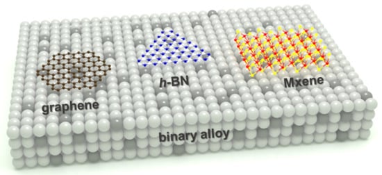
Overview of Rational Design of Binary Alloy for the Synthesis of Two-Dimensional Materials
by
 ,
,
Hongyan Zhu
1,2,3, 
Chao Zhang
1,2,3,
Xuefu Zhang
1,3,
Zhiyuan Shi
1,3,*,
Tianru Wu
1,3,* and
Guanghui Yu
1,3 1
State Key Laboratory of Functional Materials for Informatics, Shanghai Institute of Microsystem and Information Technology, Chinese Academy of Sciences, 865 Changning Road, Shanghai 200050, China
2
School of Electronic, Electrical and Communication Engineering, University of Chinese Academy of Sciences, 19 A Yuquan Road, Beijing 100049, China
3
CAS Center for Excellence in Superconducting Electronics (CENSE), 865 Changning Road, Shanghai 200050, China
*
Authors to whom correspondence should be addressed.
Surfaces 2020, 3(1), 26-39; https://doi.org/10.3390/surfaces3010003
Submission received: 15 November 2019
/
Revised: 4 January 2020
/
Accepted: 13 January 2020
/
Published: 15 January 2020
(This article belongs to the Special Issue Surface Science and Catalysis of Graphene-Related 2D Materials)
Abstract
:Two-dimensional (2D) materials attracted widespread interest as unique and novel properties different from their bulk crystals, providing great potential for semiconductor devices and applications. Recently, the family of 2D materials has been expanded including but not limited to graphene, hexagonal boron nitride (h-BN), transition metal carbides (TMCs), and transition metal dichalcogenides (TMDCs). Metal-catalyzed chemical vapor deposition (CVD) is an effective method to achieve precise synthesis of these 2D materials. In this review, we focus on designing various binary alloys to realize controllable synthesis of multiple CVD-grown 2D materials and their heterostructures for both fundamental research and practical applications. Further investigations indicated that the design of the catalytic substrate is an important issue, which determines the morphology, domain size, thickness and quality of 2D materials and their heterostructures.
1. Introduction
Since graphene was first successfully prepared by mechanical exfoliation from graphite [1], two-dimensional (2D) materials have attracted extensive attention due to their unique structural and physical properties [2,3,4]. The extensive family of 2D materials, including conductors [5,6], semiconductors with various bandgaps [7,8] and insulators [9,10], exhibited extraordinary electronical and optical performance in contrast to their bulk counterparts. For semiconductor applications, van der Waals heterostructures constructed from stacking of various 2D materials have been assembled, utilizing different properties of individual 2D crystals to create new physical characteristics and unique functionalities [11,12,13]. In order to realize the heterogeneous integration at the atomic scale, controllable synthesis of 2D materials and heterostructures is of great importance for both fundamental researches and technological applications. Over the past decade, chemical vapor deposition (CVD) has achieved a huge success for several well-known 2D materials, which have been developed extensively for large-scale practical applications [14]. In particular, catalytic substrate engineering plays a significant role in the CVD process for controlling the domain size, thickness, morphology, and surface quality of various 2D materials [15].
During the synthesis process of 2D materials, metal acts as a promising catalyst, an epitaxial substrate, and sometimes a dissolution source of the reaction atoms. In previous reports, metal substrates such as Cu [16,17], Ni [18], Pt [19], Ru [20], etc. with various catalytic properties and different solubility of specific atoms have been extensively studied to obtain uniform, large-area and high quality 2D materials. In previous reports, surface-limited growth process induced monolayer graphene on Au [21], Pt [19], and Cu [16,17] due to the negligible solubility of reaction atoms. Multilayer graphene films were obtained on Fe [22], Co [23], and Ni [18] because of the cooling induced precipitation of dissolved atoms in these transition metals. However, the catalytic growth of wafer scale single crystalline 2D materials and scalable construction of complex heterostructures with designed spatial modulation on single component metal are still challenging. Thus, by rationally designing the composition, proportion and crystal orientation of binary alloys, various metals with different catalytic properties could be combined to develop a facile and controllable strategy to achieve the scalable CVD fabrication. In this review, we highlight the recent progress on the investigations of designing binary alloys for controlled growth of single crystal 2D materials and their heterostructures. We also study the roles of each catalytic component during the growth process through various surface analytic characterizations. In general, the present strategy can be extended to any well-defined alloys, which will greatly facilitate the controllable construction of various 2D heterostructures for practical applications.
2. Synthesis of Graphene on Cu-Ni Alloy
Among the most widely applied metal catalysts for graphene synthesis, Cu and Ni show completely different catalytic mechanism [24,25]. The growth of graphene on Cu follows the surface-mediated mechanism which makes Cu an ideal substrate for monolayer graphene synthesis [16,26,27]. However, the catalytic power of Cu decreased due to the gradually reduced active substrate during the growth procedure, resulting in the low growth rate and difficulty for multilayer graphene growth. In contrast, graphene growth on Ni follows the dissolution–precipitation mechanism, which can promote carbon supply. However, the segregation of the dissolved carbon atoms normally induces the randomly stacked non-uniform multilayers [28]. Because Cu and Ni can form solid solutions in the full range of concentration, some research groups found that the Cu-Ni alloy could combine the advantages of both catalysts, making it easier to control the uniformity and layer number of graphene. Meanwhile, the decomposition of methane and carbon solubility in the alloy enhanced with increasing Ni content. It induced the transition from a two-dimensional surface diffusion to a quasi-three-dimensional carbon diffusion in the bulk. The large amount of isolated active carbon atoms in the sub-surface obviously promoted the growth rate of graphene by the change of growth mechanism from surface-mediated growth to the isothermal segregation process [29].
An epitaxial growth approach for wafer-sized monolayer graphene on Cu-Ni alloy was reported by Zhang et al. [30]. In this report, Cu-Ni films were deposited onto α-Al2O3 (0001) wafer, and the subsequent annealing process allowed single crystallization of Cu-Ni (111)-oriented texture as well as the reduction of surface roughness (Figure 1a). It was demonstrated that uniform and wrinkle free single-crystal graphene was obtained at a relatively low temperature of 750 °C. The atomic force microscopy (AFM) image showed that the root mean square (RMS) value was around 0.6 nm in the 100 μm2 area, which indicated the ultra-flat surface (Figure 1b). Vlassiouk et al. further succeed in fabricating single-crystal graphene on a polycrystalline Cu-Ni substrate through advancing local control of the precursor concentrations CVD method based on “evolutionary selection” [31]. According to the schematic illustration in Figure 1c, the dominant graphene domain extended forwards and gradually surpassed neighboring competitors, forming a single survivor-monocrystal over a large area eventually. By using local feeding via a small nozzle, high velocity flowing buffer gases, and removable Cu90Ni10 alloy substrates, the upstream residual seeds could be completely eliminated, allowing the synthesis of a foot-long single crystal graphene film (as shown in Figure 1d). As another synthetic method similar to silicon ingot growth, Wu et al. utilized the local precursor feeding method (shown in the inset of Figure 1e) and successfully achieved a single graphene nucleus on the Cu-Ni alloy substrate [32]. The secondary ion mass spectrometry (SIMS) line scan profiles indicated that the local carbon concentration on the surface of alloy tended to decrease along the gradient distribution outward from the center (Figure 1e). The authors investigated the growth rate of graphene domain on the Cu-Ni alloy with different compositions. Much higher growth rate would be realized with increasing Ni content due to the abundant active carbon atoms dissolved in Cu85Ni15 alloy. However, for Ni content approaching or higher than the percolation threshold, carbon atoms tend to diffuse into the depth of alloy, which induced a decreased growth rate (Figure 1f). This work realized the fast growth of ~1.5-inch single crystalline graphene in 2.5 h (Figure 1g).
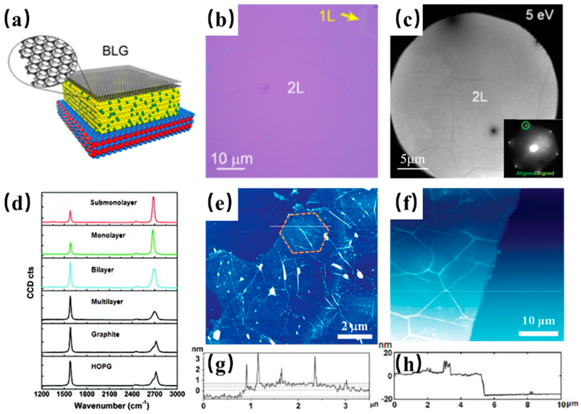
Moreover, Cu-Ni alloy could control the solubility of carbon by adjusting the concentration of Ni in the alloy. The controllable growth of graphene with high uniformity and different layers has been achieved. Takesaki et al. demonstrated the synthesis of uniform bilayer graphene with coverage up to 93% on Cu-Ni (111) films (Figure 2a) [33]. The optical image and bright-field (BF) low energy electron microscopy (LEEM) image showed uniform contrast in the whole view area, indicating the realization of large scale and uniform bilayer graphene (Figure 2b,c). Meanwhile, in the inset of Figure 2c, only one set of hexagonal diffraction spots was observed, indicating the existence of AB stacking. In addition, Chen et al. reported the synthesis of multilayer graphene on Cu-Ni foil [34]. The thickness and quality of the graphene films could be controlled by modulating the deposition temperature and cooling rate. Raman spectra combined with AFM height images and profiles provided strong evidence that the thickness of the prepared graphene covered from single layer to around 19 nm (Figure 2d–h). In conclusion, Cu-Ni alloys provide a highly catalytic and smooth-faced substrate with controllable carbon solubility, which enables the scalable preparation and further application of large-area and high-quality graphene.
3. Synthesis of h-BN on Binary Alloy
Similar to graphene growth, synthesis of h-BN on metals via CVD is also a heterogeneous catalytic chemical reaction process. By designing the composition and proportion of binary alloy, controllability of layer thickness, domain size, and even morphology of h-BN has been realized.
Recently, Lu et al. demonstrated that Cu-Ni alloy was also a good candidate for growing large-area h-BN single crystals via the low pressure CVD (LPCVD) process (Figure 3a) [35]. It was illustrated that appropriate proportion of Ni could enhance the decomposition of by products such as poly-aminoborane. This strategy enabled nucleation density down to 60 per mm2 and h-BN grains size up to 7500 μm2 (Figure 3b). In addition, Li et al. introduced the innovative Cu-Si alloy as a catalytic substrate [36]. The Cu-Si alloy exhibited face-center cubic (FCC) structure at the growth temperature of 1030 °C, which was proved by the binary alloy phase diagram (Figure 3c). The presence of Si (≈2.8 at%) in such alloy could change the growth mechanism from edge-limited growth to diffusion-limited regime, leading to distinctive tree pattern morphologies and large domain size (Figure 3d). Furthermore, the strategy of incorporating proper concentration of Si into metal catalyst has been extended to the synthesis of single crystal h-BN on Si-doped Fe (Figure 3e). Caneva et al. revealed that, compared to Cu, an intermediate ratio of B and N atoms appeared to be maintained in the Fe catalyst [37]. The Si admixture could promote the catalytic dissociation of borazine and the growth rate of h-BN, which induced exclusive nucleation and growth of monolayer h-BN with lateral dimensions of ~0.3 mm (shown in Figure 3f) as well as continuous h-BN monolayer films with domain sizes larger than 25 µm.
Meanwhile, synthesis of multilayer h-BN films with specific thickness and large-area uniformity is in general highly desired for practical device applications. Previously, Uchida et al. succeeded in the preparation of large area multilayer h-BN on Ni-Fe film (Figure 3g) [38]. It was found that Fe was a potential substrate to form multilayer h-BN due to its relative high solubilities of both B and N atoms. The Ni phase in Fe films could stabilize the FCC structure and control the solubilities of B and N atoms, which promoted the uniform segregation of multilayer h-BN. The cross-sectional TEM of as-grown thin films on alloy showed high uniformity of h-BN layers with thickness of 2–5 nm (Figure 3h). Recently, Shi et al. developed a new method to synthesize multilayer h-BN by using Fe-B alloy and N2 as reactants (Figure 3i) [39]. The growth procedure broke the traditional self-limited growth mechanism on catalytic metal substrates and successfully obtained large scale multilayer h-BN films. As shown in Figure 3j, the SEM and AFM image exhibited a uniform and thickness controllable multilayer h-BN on the Fe2B substrate. The HRTEM image displayed the lattice fringe and a well-defined layer structure of h-BN multilayers (Figure 3k,l). Corresponding selected area electron diffraction (SAED) presented one set of hexagonally arranged spots, indicating the highly oriented alignment of multilayer h-BN films. In conclusion, a precise design of alloy catalyst will provide a promising strategy for the mass production of h-BN.
4. Other 2D Materials Grown on Binary Alloy
The exploration and synthesis of other novel 2D materials have expanded to new areas of research owing to their fascinating physical properties and potential applications. Among them, 2D binary compounds termed MXn, where M is typically a transition metal and X is a non-metal from main groups IV, V, or VI, were found to be suitable candidates for semiconductor-based electronics and optoelectronics applications [40,41,42]. In this regard, the vapor phase-based growth approaches provide a scalable and controllable way to grow high quality and large area 2D MXn on binary alloys.
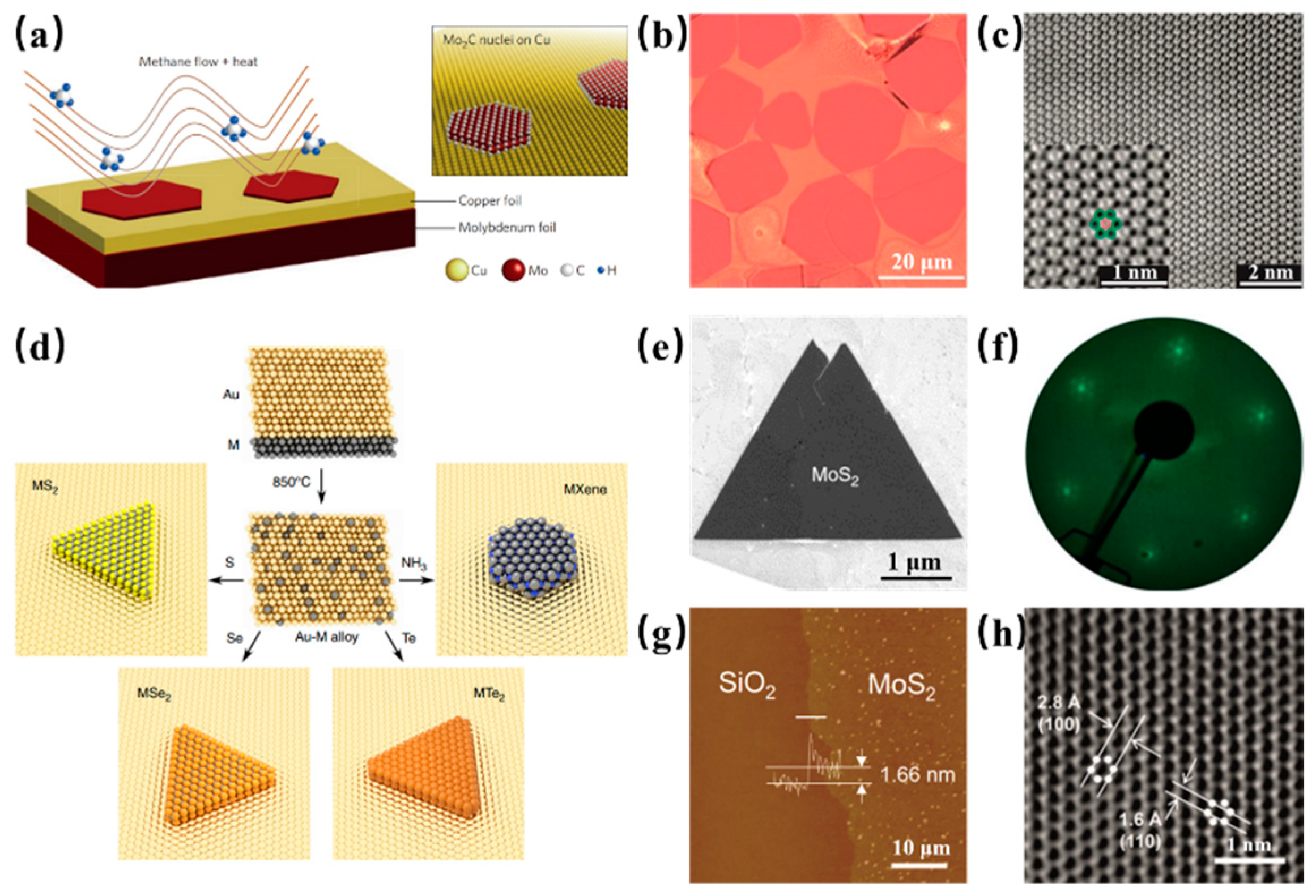
Recently, Xu et al. developed a Cu-Mo alloy as the catalytic substrate to grow high-quality 2D ultrathin α-Mo2C crystals with a uniform thickness of ~3 nm [43]. Some Mo atoms diffused to the surface of the liquid Cu to form Mo2C crystals by reacting with the carbon atoms from the decomposition of methane (Figure 4a). As shown in Figure 4b, the ultrathin α-Mo2C sheets exhibited different but all regular shapes, suggesting that the crystals were well-defined. From the BF scanning transmission electron microscopy (STEM) image (Figure 4c), a highly-ordered orthorhombic structure formed by C and Mo atoms was clearly observed, which indicated the high quality of ultrathin α-Mo2C crystals. By increasing the concentration of methane, Geng et al. first assembled graphene domains on the surface of liquid Cu-Mo alloy, which was exhibited to be an important role in controlling the shape of Mo2C crystals [44]. Thus, large-scale Mo2C crystals with high uniformity and regular edges have been obtained on graphene films. In addition, Wang et al. demonstrated that this method was also applicable to the growth of various 2D Ta-compounds [45]. The synthesis of ultrathin TaC, TaN, and TaB crystals with the thickness of 8, 5, and 15 nm, respectively, was realized on the Cu-Ta alloy.
Furthermore, Shivayogimath et al. proposed a universal strategy for synthesizing thin layers of MXn on a binary alloy catalyst (Figure 4d) [47]. They arranged alloying process of metal M and gold, forming a single-phase Au-M alloy, which had limited solubilities of the X elements mentioned above. During the synthesis process subsequently, the Au-M alloy was exposed to a vapor-phase precursor containing X, then epitaxial oriented few-atom thick layers of MXn binary compounds could form on the solid–gas interface. In this work, individual MoS2 domains were first synthesized as a benchmark, which displayed typical triangular morphology (Figure 4e). The well epitaxial alignment on the alloy substrate was confirmed by low energy electron diffraction (LEED) (Figure 4f). In addition, more than 20 other binary compounds including tellurides, selenides, and nitrides were synthesized, confirming the feasibility and universality of this method. A similar synthesis approach has been achieved by Song et al. [48]. Large-scale and patterned MoS2 atomic layers have been acquired on an Au-Mo alloy, which was prepared by the reaction of Au thin film and Mo(CO)6 followed by the reaction with H2S. The height of MoS2 layers transferred onto a SiO2/Si substrate was 1.66 nm, which was consistent with the height of two or three layers of MoS2 (Figure 4g). In addition, a Fourier-filtered HRTEM image displayed an ordered hexagonal symmetry of dots, indicating the crystal structure of MoS2 (Figure 4h).
Graphene-like 2D mono-element materials, such as silicene and germanene, are also important members of the 2D family. Binary alloy could also be a great candidate for their synthesis. Silicene has been found to exist in epitaxial forms on ZrB2 (0001) [49,50] and ZrC (111) [51]. Meanwhile, binary alloys here were chosen to stabilize silicene films due to their non-negligible interactions, rather than their catalytic performance during the synthesis process. Recently, Bampoulis et al. reported the fabrication of germanene on Ge2Pt alloy [52]. The Pt layers were first deposited on Ge (110), and surface alloy nanocrystals composed of Ge2Pt were formed subsequently on the Ge substrate by annealing. Germanene was found to be synthesized as the outermost layer of Ge2Pt nanocrystals. Overall, reasonable selection and design of binary alloy as not only the catalyst, but also an ideal substrate will provide a promising strategy for the synthesis and structural regulation of 2D materials beyond graphene.
5. 2D Heterostructures Assembled on a Binary Alloy
Assembling two-dimensional materials into van der Waals heterostructures is an effective way to expand the crystal structures, physical properties and potential applications for 2D devices [12,53,54,55]. New 2D heterostructures not only overcome the inherent limitations of individual 2D materials, but also provide unique platforms to create novel properties by their proper combination. The construction of such heterostructures was usually synthesized by the following methods: (i) Layer-by-layer transfer of exfoliated 2D layers [56]; (ii) Heterogeneous stacking of CVD grown 2D materials with mechanically exfoliated 2D materials [57,58]; and (iii) Sequential growth of two-dimensional materials by introducing different gas phase precursors [59,60,61]. As a bottom-up strategy, a transfer free CVD approach realized the sequential growth or lateral coherence of monolayers with an ultra clean interface, which was considered as an ideal technique for synthesis of both vertical and in-plane van der Waals heterostructures [62,63,64].
Graphene/hexagonal boron nitride (denoted as Gr/h-BN) is the most common layered 2D heterostructures. Similar atomic arrangements and lattice constants allow precision stitching of graphene and h-BN. The completely different electronic properties make their heterostructures have many unique transport properties. Through sequential CVD growth of h-BN and graphene single-crystals, Lu et al. successfully fabricated large-area Gr/h-BN in-plane heterostructure on Cu-Ni alloy (Figure 5a) [65]. During the synthesis procedure, graphene nucleated at the corners of the as-grown h-BN grains and grown along the lattice orientation of h-BN. As shown in Figure 5b, well-assembled Gr/h-BN in-plane heterostructure was successfully synthesized on Cu-Ni substrate. In addition, auger electron spectroscopy (AES) spectra, displayed in Figure 5c, was utilized to confirm the spatial distribution of specific elements in such heterostructure. Subsequently, the vertical heterostructure was further obtained underneath an Gr/h-BN in-plane heterostructure layer (Figure 5d) [66]. The SEM image (Figure 5e) and corresponding AES spectra (Figure 5f) revealed that the graphene adlayers tended to nucleate and extend along the h-BN-Gr boundaries.
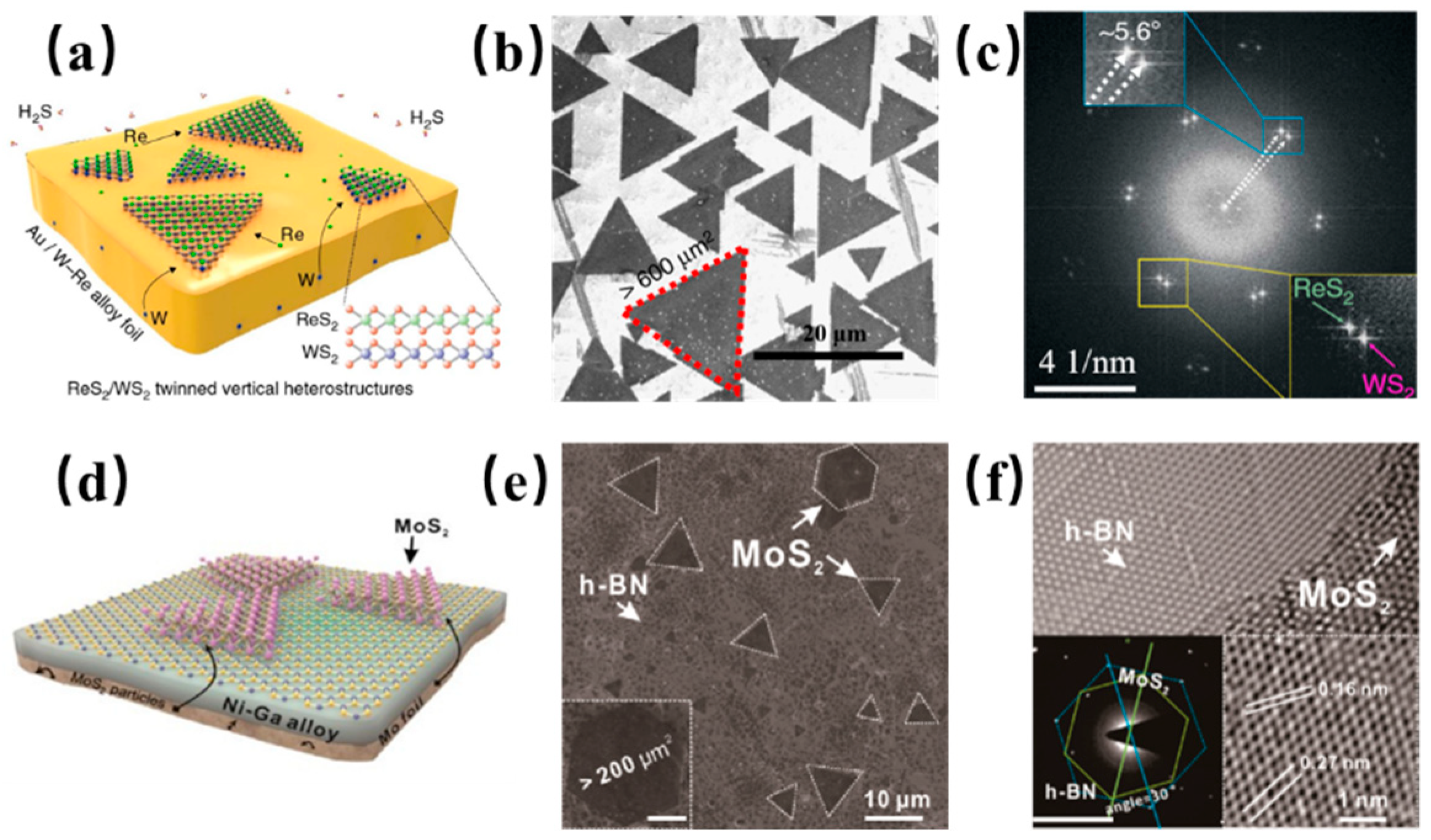
Moreover, the rational stacking of transition metal dichalcogenides (TMDCs) has attracted significant attention as it tends to expand pristine properties of individual TMDC crystals [67,68,69]. Zhang et al. utilized Au foil and binary W-Re alloy foil as the substrate and precursors [69]. As displayed in Figure 6a, by introducing H2S, twinned growth of ReS2/WS2 vertically stacked heterostructures was realized. The SEM image in Figure 6b showed that a high yield of uniform larger-area vertically stacked ReS2/WS2 crystals with the domain size of 600 μm2 were obtained by a direct CVD approach. Fast Fourier transform (FFT) patterns exhibited in Figure 6c revealed that the two hexagonal reciprocal lattices representing ReS2 and WS2 were rotated by ϕ = 5.6°. The negligible mismatch of two constituent layers proved a very high quality of twinned heterostructure.
Furthermore, improved electrical performance could be realized when stacking TMDC materials were directly grown on h-BN substrate. Therefore, the fabrication of TMDCs/h-BN heterostructures by a CVD technique attracted extensive research [64,70,71,72]. However, a great challenge for heterostructure synthesis attributed to the sulfide reaction of the metal substrate, which resulted in the decomposition of the pre-grown TMDCs/h-BN heterostructures. To address this problem, Fu et al. constructed a Ni-Ga alloy with excellent sulfide-resistance and high catalytic activity, and successfully achieved CVD growth of MoS2/h-BN heterostructures (Figure 6d) [70]. It was worth mentioning that the Mo foil beneath the Ni-Ga alloy also served as the precursor for MoS2 growth. Through that, single-crystal MoS2 was grown directly on h-BN substrates with grain sizes up to 200 μm2 (Figure 6e), which was also proved by TEM and SAED measurements (Figure 6f). In addition, the decomposition energy of h-BN on Ni-Ga was proved to be 3.9 eV, which was higher than that on Ni by DFT calculation. It indicated that the component of Ga in the alloy improved the stability of h-BN adsorbed on the surface.
6. Conclusions
In summary, we review the recent progress in the rational design of binary alloys for controllable synthesis of two-dimensional materials and their heterostructures. The selected catalytic binary alloy and various 2D materials are summarized in Table 1. In general, the functions of binary alloys could be described as follows: (i) the metal or non-metallic elements were deposited on the catalytic metal substrate, assisting to enhance its catalytic activity or adjust its crystal structure; (ii) the solubility of the desired atoms in catalytic metal could be regulated by introducing another metal with lower solubility, which could control the nucleation density and layers of CVD grown 2D materials; (iii) the active atoms on surface of substrate diffused through another up layer of catalytic films, and reacted with gaseous precursors by vapor–solid reactions. By suitable design of the catalytic binary alloys, the presented approach will show great potential for high-quality and controllable fabrication of 2D heterostructures with a well-defined distribution, which is highly significant for future applications in electronics and optoelectronics.
Author Contributions
Conceptualization, T.W. and Z.S.; writing—original draft preparation, H.Z., C.Z., X.Z., and Z.S.; writing—review and editing, H.Z., Z.S., T.W., and G.Y.; supervision, T.W.; project administration, Z.S. and T.W.; funding acquisition, T.W. All authors have read and agreed to the published version of the manuscript.
Funding
This research was funded by the National Key R&D program, Grant No. 2017YFF0206106, the National Natural Science Foundation of China, Grant No. 51772317, the Strategic Priority Research Program of Chinese Academy of Sciences, Grant No. XDB30000000, the Science and Technology Commission of Shanghai Municipality, Grant Nos. 16ZR1442700 and 18511110700, and the Shanghai Rising-Star Program (A type), Grant No. 18QA1404800.
Conflicts of Interest
The authors declare no conflict of interest.
Abbreviations
| 2D | Two-dimensional |
| h-BN | Hexagonal boron nitride |
| TMC | Transition metal carbide |
| TMDCs | Transition metal dichalcogenides |
| CVD | Chemical vapor deposition |
| AFM | Atomic force microscopy |
| RMS | Root mean square |
| SIMS | Secondary ion mass spectrometry |
| BF | Bright field |
| LEEM | Low energy electron microscopy |
| LPCVD | Low-pressure chemical vapor deposition |
| FCC | Face-center cubic |
| SEM | Scanning electron microscope |
| TEM | Transmission electron microscopy |
| HRTEM | High resolution transmission electron microscopy |
| SAED | Selected area electron diffraction |
| STEM | Scanning transmission electron microscopy |
| LEED | Low energy electron diffraction |
| FFT | Fast Fourier transform |
| AES | Auger electron spectroscopy |
| Gr/h-BN | Graphene/hexagonal boron nitride heterostructure |
| APCVD | Atmospheric pressure chemical vapor deposition |
References
- Novoselov, K.S.; Geim, A.K.; Morozov, S.V.; Jiang, D.; Zhang, Y.; Dubonos, S.V.; Grigorieva, I.V.; Firsov, A.A. Electric field effect in atomically thin carbon films. Science 2004, 306, 666–669. [Google Scholar] [CrossRef] [PubMed] [Green Version]
- Lien, D.-H.; Kang, J.S.; Amani, M.; Chen, K.; Tosun, M.; Wang, H.-P.; Roy, T.; Eggleston, M.S.; Wu, M.C.; Dubey, M.; et al. Engineering Light Outcoupling in 2D Materials. Nano Lett. 2015, 15, 1356–1361. [Google Scholar] [CrossRef] [PubMed]
- Zhang, X.; Hou, L.; Ciesielski, A.; Samori, P. 2D Materials Beyond Graphene for High-Performance Energy Storage Applications. Adv. Energy Mater. 2016, 6, 1600671. [Google Scholar] [CrossRef] [Green Version]
- Xu, X.; Chen, J.; Li, B. Phonon thermal conduction in novel 2D materials. J. Phys. Condens. Matter 2016, 28, 48. [Google Scholar] [CrossRef]
- Wang, H.; Huang, X.; Lin, J.; Cui, J.; Chen, Y.; Zhu, C.; Liu, F.; Zeng, Q.; Zhou, J.; Yu, P.; et al. High-quality monolayer superconductor NbSe2 grown by chemical vapour deposition. Nat. Commun. 2017, 8, 394. [Google Scholar] [CrossRef] [PubMed]
- Wang, L.; Zhu, Y.; Wang, J.-Q.; Liu, F.; Huang, J.; Meng, X.; Basset, J.-M.; Han, Y.; Xiao, F.-S. Two-dimensional gold nanostructures with high activity for selective oxidation of carbon-hydrogen bonds. Nat. Commun. 2015, 6, 6957. [Google Scholar] [CrossRef] [PubMed] [Green Version]
- Lee, Y.-H.; Zhang, X.-Q.; Zhang, W.; Chang, M.-T.; Lin, C.-T.; Chang, K.-D.; Yu, Y.-C.; Wang, J.T.-W.; Chang, C.-S.; Li, L.-J.; et al. Synthesis of Large-Area MoS2 Atomic Layers with Chemical Vapor Deposition. Adv. Mater. 2012, 24, 2320–2325. [Google Scholar] [CrossRef] [Green Version]
- Smith, J.B.; Hagaman, D.; Ji, H.-F. Growth of 2D black phosphorus film from chemical vapor deposition. Nanotechnology 2016, 27, 21. [Google Scholar] [CrossRef]
- Shi, Y.; Hamsen, C.; Jia, X.; Kim, K.K.; Reina, A.; Hofmann, M.; Hsu, A.L.; Zhang, K.; Li, H.; Juang, Z.-Y.; et al. Synthesis of Few-Layer Hexagonal Boron Nitride Thin Film by Chemical Vapor Deposition. Nano Lett. 2010, 10, 4134–4139. [Google Scholar] [CrossRef]
- Zhuang, A.; Li, J.-J.; Wang, Y.-C.; Wen, X.; Lin, Y.; Xiang, B.; Wang, X.; Zeng, J. Screw-Dislocation-Driven Bidirectional Spiral Growth of Bi2Se3 Nanoplates. Angew. Chem. Int. Ed. 2014, 53, 6425–6429. [Google Scholar] [CrossRef]
- Geim, A.K.; Grigorieva, I.V. Van der Waals heterostructures. Nature 2013, 499, 419–425. [Google Scholar] [CrossRef] [PubMed]
- Iannaccone, G.; Bonaccorso, F.; Colombo, L.; Fiori, G. Quantum engineering of transistors based on 2D materials heterostructures. Nat. Nanotechnol. 2018, 13, 183–191. [Google Scholar] [CrossRef] [PubMed]
- Chen, K.; Wan, X.; Wen, J.; Xie, W.; Kang, Z.; Zeng, X.; Chen, H.; Xu, J.-B. Electronic Properties of MoS2-WS2 Heterostructures Synthesized with Two-Step Lateral Epitaxial Strategy. ACS Nano 2015, 9, 9868–9876. [Google Scholar] [CrossRef] [PubMed]
- Novoselov, K.S.; Fal’ko, V.I.; Colombo, L.; Gellert, P.R.; Schwab, M.G.; Kim, K. A roadmap for graphene. Nature 2012, 490, 192–200. [Google Scholar] [CrossRef] [PubMed]
- Tan, L.; Zeng, M.; Zhang, T.; Fu, L. Design of catalytic substrates for uniform graphene films: From solid-metal to liquid-metal. Nanoscale 2015, 7, 9105–9121. [Google Scholar] [CrossRef] [PubMed]
- Li, X.; Cai, W.; An, J.; Kim, S.; Nah, J.; Yang, D.; Piner, R.; Velamakanni, A.; Jung, I.; Tutuc, E.; et al. Large-Area Synthesis of High-Quality and Uniform Graphene Films on Copper Foils. Science 2009, 324, 1312–1314. [Google Scholar] [CrossRef] [Green Version]
- Wang, L.; Wu, B.; Jiang, L.; Chen, J.; Li, Y.; Guo, W.; Hu, P.; Liu, Y. Growth and Etching of Monolayer Hexagonal Boron Nitride. Adv. Mater. 2015, 27, 4858–4864. [Google Scholar] [CrossRef]
- Kim, K.S.; Zhao, Y.; Jang, H.; Lee, S.Y.; Kim, J.M.; Kim, K.S.; Ahn, J.-H.; Kim, P.; Choi, J.-Y.; Hong, B.H. Large-scale pattern growth of graphene films for stretchable transparent electrodes. Nature 2009, 457, 706–710. [Google Scholar] [CrossRef]
- Gao, L.; Ren, W.; Xu, H.; Jin, L.; Wang, Z.; Ma, T.; Ma, L.-P.; Zhang, Z.; Fu, Q.; Peng, L.-M.; et al. Repeated growth and bubbling transfer of graphene with millimetre-size single-crystal grains using platinum. Nat. Commun. 2012, 3, 699. [Google Scholar] [CrossRef]
- Sutter, E.; Albrecht, P.; Sutter, P. Graphene growth on polycrystalline Ru thin films. Appl. Phys. Lett. 2009, 95, 133109. [Google Scholar] [CrossRef]
- Nie, S.; Bartelt, N.C.; Wofford, J.M.; Dubon, O.D.; McCarty, K.F.; Thuermer, K. Scanning tunneling microscopy study of graphene on Au(111): Growth mechanisms and substrate interactions. Phys. Rev. B 2012, 85, 205406. [Google Scholar] [CrossRef] [Green Version]
- An, H.; Lee, W.-J.; Jung, J. Graphene synthesis on Fe foil using thermal CVD. Curr. Appl. Phys. 2011, 11, S81–S85. [Google Scholar] [CrossRef]
- Kim, E.; An, H.; Jang, H.; Cho, W.-J.; Lee, N.; Lee, W.-G.; Jung, J. Growth of Few-Layer Graphene on a Thin Cobalt Film on a Si/SiO2 Substrate. Chem. Vap. Depos. 2011, 17, 9–14. [Google Scholar] [CrossRef]
- Ago, H.; Ogawa, Y.; Tsuji, M.; Mizuno, S.; Hibino, H. Catalytic Growth of Graphene: Toward Large-Area Single-Crystalline Graphene. J. Phys. Chem. Lett. 2012, 3, 2228–2236. [Google Scholar] [CrossRef] [PubMed]
- Patera, L.L.; Africh, C.; Weatherup, R.S.; Blume, R.; Bhardwaj, S.; Castellarin-Cudia, C.; Knop-Gericke, A.; Schloegl, R.; Comelli, G.; Hofmann, S.; et al. In Situ Observations of the Atomistic Mechanisms of Ni Catalyzed Low Temperature Graphene Growth. ACS Nano 2013, 7, 7901–7912. [Google Scholar] [CrossRef] [Green Version]
- Wang, H.; Wang, G.; Bao, P.; Yang, S.; Zhu, W.; Xie, X.; Zhang, W.-J. Controllable Synthesis of Submillimeter Single-Crystal Monolayer Graphene Domains on Copper Foils by Suppressing Nucleation. J. Am. Chem. Soc. 2012, 134, 3627–3630. [Google Scholar] [CrossRef]
- Yan, Z.; Lin, J.; Peng, Z.; Sun, Z.; Zhu, Y.; Li, L.; Xiang, C.; Samuel, E.L.; Kittrell, C.; Tour, J.M. Toward the Synthesis of Wafer-Scale Single-Crystal Graphene on Copper Foils. ACS Nano 2012, 6, 9110–9117. [Google Scholar] [CrossRef]
- Yu, Q.; Lian, J.; Siriponglert, S.; Li, H.; Chen, Y.P.; Pei, S.-S. Graphene segregated on Ni surfaces and transferred to insulators. Appl. Phys. Lett. 2008, 93, 113103. [Google Scholar] [CrossRef] [Green Version]
- Liu, Y.; Wu, T.; Yin, Y.; Zhang, X.; Yu, Q.; Searles, D.J.; Ding, F.; Yuan, Q.; Xie, X. How Low Nucleation Density of Graphene on Cu-Ni Alloy is Achieved. Adv. Sci. 2018, 5, 1700961. [Google Scholar] [CrossRef]
- Zhang, X.; Wu, T.; Jiang, Q.; Wang, H.; Zhu, H.; Chen, Z.; Jiang, R.; Niu, T.; Li, Z.; Zhang, Y.; et al. Epitaxial Growth of 6 in. Single-Crystalline Graphene on a Cu/Ni (111) Film at 750 °C via Chemical Vapor Deposition. Small 2019, 15, 1805395. [Google Scholar] [CrossRef]
- Vlassiouk, I.V.; Stehle, Y.; Pudasaini, P.R.; Unocic, R.R.; Rack, P.D.; Baddorf, A.P.; Ivanov, I.N.; Lavrik, N.V.; List, F.; Gupta, N.; et al. Evolutionary selection growth of two-dimensional materials on polycrystalline substrates. Nat. Mater. 2018, 17, 318. [Google Scholar] [CrossRef]
- Wu, T.; Zhang, X.; Yuan, Q.; Xue, J.; Lu, G.; Liu, Z.; Wang, H.; Wang, H.; Ding, F.; Yu, Q.; et al. Fast growth of inch-sized single-crystalline graphene from a controlled single nucleus on Cu-Ni alloys. Nat. Mater. 2016, 15, 43. [Google Scholar] [CrossRef] [PubMed]
- Takesaki, Y.; Kawahara, K.; Hibino, H.; Okada, S.; Tsuji, M.; Ago, H. Highly Uniform Bilayer Graphene on Epitaxial Cu-Ni(111) Alloy. Chem. Mater. 2016, 28, 4583–4592. [Google Scholar] [CrossRef]
- Chen, S.; Cai, W.; Piner, R.D.; Suk, J.W.; Wu, Y.; Ren, Y.; Kang, J.; Ruoff, R.S. Synthesis and Characterization of Large-Area Graphene and Graphite Films on Commercial Cu-Ni Alloy Foils. Nano Lett. 2011, 11, 3519–3525. [Google Scholar] [CrossRef] [PubMed]
- Lu, G.; Wu, T.; Yuan, Q.; Wang, H.; Wang, H.; Ding, F.; Xie, X.; Jiang, M. Synthesis of large single-crystal hexagonal boron nitride grains on Cu-Ni alloy. Nat. Commun. 2015, 6, 6160. [Google Scholar] [CrossRef] [PubMed]
- Li, J.; Hu, Z.; Yi, Y.; Yu, M.; Li, X.; Zhou, J.; Yin, J.; Wu, S.; Guo, W. Hexagonal Boron Nitride Growth on Cu-Si Alloy: Morphologies and Large Domains. Small 2019, 15, 1805188. [Google Scholar] [CrossRef] [PubMed]
- Caneva, S.; Weatherup, R.S.; Bayer, B.C.; Brennan, B.; Spencer, S.J.; Mingard, K.; Cabrero-Vilatela, A.; Baehtz, C.; Pollard, A.J.; Hofmann, S. Nucleation Control for Large, Single Crystalline Domains of Mono layer Hexagonal Boron Nitride via Si-Doped Fe Catalysts. Nano Lett. 2015, 15, 1867–1875. [Google Scholar] [CrossRef]
- Uchida, Y.; Nakandakari, S.; Kawahara, K.; Yamasaki, S.; Mitsuhara, M.; Ago, H. Controlled Growth of Large-Area Uniform Multilayer Hexagonal Boron Nitride as an Effective 2D Substrate. ACS Nano 2018, 12, 6236–6244. [Google Scholar] [CrossRef]
- Shi, Z.; Lu, G.; Yang, P.; Wu, T.; Yin, W.; Zhang, C.; Jiang, R.; Xie, X. Controlled synthesis of uniform multilayer hexagonal boron nitride films on Fe2B alloy. RSC Adv. 2019, 9, 10155–10158. [Google Scholar] [CrossRef] [Green Version]
- Butler, S.Z.; Hollen, S.M.; Cao, L.; Cui, Y.; Gupta, J.A.; Gutierrez, H.R.; Heinz, T.F.; Hong, S.S.; Huang, J.; Ismach, A.F.; et al. Progress, Challenges, and Opportunities in Two-Dimensional Materials Beyond Graphene. ACS Nano 2013, 7, 2898–2926. [Google Scholar] [CrossRef]
- Zhong, Y.; Xia, X.; Shi, F.; Zhan, J.; Tu, J.; Fan, H.J. Transition Metal Carbides and Nitrides in Energy Storage and Conversion. Adv. Sci. 2016, 3, 1500286. [Google Scholar] [CrossRef]
- Hantanasirisakul, K.; Gogotsi, Y. Electronic and Optical Properties of 2D Transition Metal Carbides and Nitrides (MXenes). Adv. Mater. 2018, 30, 1804779. [Google Scholar] [CrossRef]
- Xu, C.; Wang, L.; Liu, Z.; Chen, L.; Guo, J.; Kang, N.; Ma, X.-L.; Cheng, H.-M.; Ren, W. Large-area high-quality 2D ultrathin Mo2C superconducting crystals. Nat. Mater. 2015, 14, 1135. [Google Scholar] [CrossRef]
- Geng, D.; Zhao, X.; Chen, Z.; Sun, W.; Fu, W.; Chen, J.; Liu, W.; Zhou, W.; Loh, K.P. Direct Synthesis of Large-Area 2D Mo2C on In Situ Grown Graphene. Adv. Mater. 2017, 29, 1700072. [Google Scholar] [CrossRef]
- Wang, Z.; Kochat, V.; Pandey, P.; Kashyap, S.; Chattopadhyay, S.; Samanta, A.; Sarkar, S.; Manimunda, P.; Zhang, X.; Asif, S.; et al. Metal Immiscibility Route to Synthesis of Ultrathin Carbides, Borides, and Nitrides. Adv. Mater. 2017, 29, 1700364. [Google Scholar] [CrossRef]
- Gogotsi, Y. Chemical Vapour Deposition Transition metal carbides go 2D. Nat. Mater. 2015, 14, 1079–1080. [Google Scholar] [CrossRef]
- Shivayogimath, A.; Thomsen, J.D.; Mackenzie, D.M.A.; Geisler, M.; Stan, R.-M.; Holt, A.J.; Bianchi, M.; Crovetto, A.; Whelan, P.R.; Carvalho, A.; et al. A universal approach for the synthesis of two-dimensional binary compounds. Nat. Commun. 2019, 10, 2957. [Google Scholar] [CrossRef] [Green Version]
- Song, I.; Park, C.; Hong, M.; Baik, J.; Shin, H.-J.; Choi, H.C. Patternable Large-Scale Molybdenium Disulfide Atomic Layers Grown by Gold-Assisted Chemical Vapor Deposition. Angew. Chem. Int. Ed. 2014, 53, 1266–1269. [Google Scholar] [CrossRef] [PubMed]
- Fleurence, A.; Gill, T.G.; Friedlein, R.; Sadowski, J.T.; Aoyagi, K.; Copel, M.; Tromp, R.M.; Hirjibehedin, C.F.; Yamada-Takamura, Y. Single-domain epitaxial silicene on diboride thin films. Appl. Phys. Lett. 2016, 108, 151902. [Google Scholar] [CrossRef] [Green Version]
- Fleurence, A.; Friedlein, R.; Ozaki, T.; Kawai, H.; Wang, Y.; Yamada-Takamura, Y. Experimental Evidence for Epitaxial Silicene on Diboride Thin Films. Phys. Rev. Lett. 2012, 108, 245501. [Google Scholar] [CrossRef] [PubMed]
- Aizawa, T.; Suehara, S.; Otani, S. Silicene on Zirconium Carbide (111). J. Phys. Chem. C 2014, 118, 23049–23057. [Google Scholar] [CrossRef]
- Bampoulis, P.; Zhang, L.; Safaei, A.; van Gastel, R.; Poelsema, B.; Zandvliet, H.J.W. Germanene termination of Ge2Pt crystals on Ge (110). J. Phys. Condens. Matter 2014, 26, 442001. [Google Scholar] [CrossRef] [PubMed] [Green Version]
- Dong, F.; Xiong, T.; Sun, Y.; Zhang, Y.; Zhou, Y. Controlling interfacial contact and exposed facets for enhancing photocatalysis via 2D-2D heterostructures. Chem. Commun. 2015, 51, 8249–8252. [Google Scholar] [CrossRef] [PubMed]
- Wilson, N.R.; Nguyen, P.V.; Seyler, K.; Rivera, P.; Marsden, A.J.; Laker, Z.P.L.; Constantinescu, G.C.; Kandyba, V.; Barinov, A.; Hine, N.D.M.; et al. Determination of band offsets, hybridization, and exciton binding in 2D semiconductor heterostructures. Sci. Adv. 2017, 3, e1601832. [Google Scholar] [CrossRef] [PubMed] [Green Version]
- Wu, Z.-S.; Zheng, Y.; Zheng, S.; Wang, S.; Sun, C.; Parvez, K.; Ikeda, T.; Bao, X.; Muellen, K.; Feng, X. Stacked-Layer Heterostructure Films of 2D Thiophene Nanosheets and Graphene for High-Rate All-Solid-State Pseudocapacitors with Enhanced Volumetric Capacitance. Adv. Mater. 2017, 29, 1602960. [Google Scholar] [CrossRef]
- Dean, C.R.; Young, A.F.; Meric, I.; Lee, C.; Wang, L.; Sorgenfrei, S.; Watanabe, K.; Taniguchi, T.; Kim, P.; Shepard, K.L.; et al. Boron nitride substrates for high-quality graphene electronics. Nat. Nanotechnol. 2010, 5, 722–726. [Google Scholar] [CrossRef]
- Tang, S.; Wang, H.; Wang, H.S.; Sun, Q.; Zhang, X.; Cong, C.; Xie, H.; Liu, X.; Zhou, X.; Huang, F.; et al. Silane-catalysed fast growth of large single-crystalline graphene on hexagonal boron nitride. Nat. Commun. 2015, 6, 6499. [Google Scholar] [CrossRef]
- Wang, J.; Yao, Q.; Huang, C.-W.; Zou, X.; Liao, L.; Chen, S.; Fan, Z.; Zhang, K.; Wu, W.; Xiao, X.; et al. High Mobility MoS2 Transistor with Low Schottky Barrier Contact by Using Atomic Thick h-BN as a Tunneling Layer. Adv. Mater. 2016, 28, 8302–8308. [Google Scholar] [CrossRef]
- Wang, M.; Jang, S.K.; Jang, W.-J.; Kim, M.; Park, S.-Y.; Kim, S.-W.; Kahng, S.-J.; Choi, J.-Y.; Ruoff, R.S.; Song, Y.J.; et al. A Platform for Large-Scale Graphene Electronics-CVD Growth of Single-Layer Graphene on CVD-Grown Hexagonal Boron Nitride. Adv. Mater. 2013, 25, 2746–2752. [Google Scholar] [CrossRef]
- Zhang, C.; Zhao, S.; Jin, C.; Koh, A.L.; Zhou, Y.; Xu, W.; Li, Q.; Xiong, Q.; Peng, H.; Liu, Z. Direct growth of large-area graphene and boron nitride heterostructures by a co-segregation method. Nat. Commun. 2015, 6, 6519. [Google Scholar] [CrossRef] [Green Version]
- Miwa, J.A.; Dendzik, M.; Gronborg, S.S.; Bianchi, M.; Lauritsen, J.V.; Hofmann, P.; Ulstrup, S. Van der Waals Epitaxy of Two-Dimensional MoS2-Graphene Heterostructures in Ultrahigh Vacuum. ACS Nano 2015, 9, 6502–6510. [Google Scholar] [CrossRef] [PubMed]
- Liu, Z.; Ma, L.; Shi, G.; Zhou, W.; Gong, Y.; Lei, S.; Yang, X.; Zhang, J.; Yu, J.; Hackenberg, K.P.; et al. In-plane heterostructures of graphene and hexagonal boron nitride with controlled domain sizes. Nat. Nanotechnol. 2013, 8, 119–124. [Google Scholar] [CrossRef] [PubMed]
- Gong, Y.; Lin, J.; Wang, X.; Shi, G.; Lei, S.; Lin, Z.; Zou, X.; Ye, G.; Vajtai, R.; Yakobson, B.I.; et al. Vertical and in-plane heterostructures from WS2/MoS2 monolayers. Nat. Mater. 2014, 13, 1135–1142. [Google Scholar] [CrossRef] [PubMed] [Green Version]
- Wang, S.; Wang, X.; Warner, J.H. All Chemical Vapor Deposition Growth of MoS2:h-BN Vertical van der Waals Heterostructures. ACS Nano 2015, 9, 5246–5254. [Google Scholar] [CrossRef] [PubMed]
- Lu, G.; Wu, T.; Yang, P.; Yang, Y.; Jin, Z.; Chen, W.; Jia, S.; Wang, H.; Zhang, G.; Sun, J.; et al. Synthesis of High-Quality Graphene and Hexagonal Boron Nitride Monolayer In-Plane Heterostructure on Cu-Ni Alloy. Adv. Sci. 2017, 4, 1700076. [Google Scholar] [CrossRef] [Green Version]
- Lu, G.; Zhang, G.; Sun, J.; Wang, X.; Shi, Z.; Jiang, D.; Wang, H.; Li, A.; Wu, T.; Yu, Q.; et al. Synthesis and stacking sequence characterization of h-BN/graphene heterostructures on Cu-Ni alloy. Carbon 2019, 152, 521–526. [Google Scholar] [CrossRef]
- Cheng, R.; Li, D.; Zhou, H.; Wang, C.; Yin, A.; Jiang, S.; Liu, Y.; Chen, Y.; Huang, Y.; Duan, X. Electroluminescence and Photocurrent Generation from Atomically Sharp WSe2/MoS2 Heterojunction p-n Diodes. Nano Lett. 2014, 14, 5590–5597. [Google Scholar] [CrossRef] [Green Version]
- Komsa, H.-P.; Krasheninnikov, A.V. Electronic structures and optical properties of realistic transition metal dichalcogenide heterostructures from first principles. Phys. Rev. B 2013, 88, 085318. [Google Scholar] [CrossRef] [Green Version]
- Zhang, T.; Jiang, B.; Xu, Z.; Mendes, R.G.; Xiao, Y.; Chen, L.; Fang, L.; Gemming, T.; Chen, S.; Ruemmeli, M.H.; et al. Twinned growth behaviour of two-dimensional materials. Nat. Commun. 2016, 7, 13911. [Google Scholar] [CrossRef]
- Fu, L.; Sun, Y.; Wu, N.; Mendes, R.G.; Chen, L.; Xu, Z.; Zhang, T.; Ruemmeli, M.H.; Rellinghaus, B.; Pohl, D.; et al. Direct Growth of MoS2/h-BN Heterostructures via a Sulfide-Resistant Alloy. ACS Nano 2016, 10, 2063–2070. [Google Scholar] [CrossRef]
- Okada, M.; Sawazaki, T.; Watanabe, K.; Taniguch, T.; Hibino, H.; Shinohara, H.; Kitaura, R. Direct Chemical Vapor Deposition Growth of WS2 Atomic Layers on Hexagonal Boron Nitride. ACS Nano 2014, 8, 8273–8277. [Google Scholar] [CrossRef] [PubMed]
- Zhang, M.; Zhu, Y.; Wang, X.; Feng, Q.; Qiao, S.; Wen, W.; Chen, Y.; Cui, M.; Zhang, J.; Cai, C.; et al. Controlled Synthesis of ZrS2 Mono layer and Few Layers on Hexagonal Boron Nitride. J. Am. Chem. Soc. 2015, 137, 7051–7054. [Google Scholar] [CrossRef] [PubMed]
- Weatherup, R.S.; Bayer, B.C.; Blume, R.; Ducati, C.; Baehtz, C.; Schloegl, R.; Hofmann, S. In Situ Characterization of Alloy Catalysts for Low-Temperature Graphene Growth. Nano Lett. 2011, 11, 4154–4160. [Google Scholar] [CrossRef] [PubMed]
- Lin, T.; Huang, F.; Wan, D.; Bi, H.; Xie, X.; Jiang, M. Self-regulating homogenous growth of high-quality graphene on Co-Cu composite substrate for layer control. Nanoscale 2013, 5, 5847–5853. [Google Scholar] [CrossRef] [PubMed]
- Ruemmeli, M.H.; Zeng, M.; Melkhanova, S.; Gorantla, S.; Bachmatiuk, A.; Fu, L.; Yan, C.; Oswald, S.; Mendes, R.G.; Makarov, D.; et al. Insights into the Early Growth of Homogeneous Single-Layer Graphene over Ni-Mo Binary Substrates. Chem. Mater. 2013, 25, 3880–3887. [Google Scholar] [CrossRef]
Figure 1.
Synthesis of single-crystal graphene on Cu-Ni alloy. (a) schematics for the fabrication of wafer-scale single-crystal graphene on Cu-Ni (111) film; (b) atomic force microscopy (AFM) height image of epitaxial graphene on Cu-Ni (111) [30]; (c) schematic illustration of evolutionary selection during the advancing local control chemical vapor deposition process for the growth of graphene grains; (d) optical image of the foot-long single crystal graphene film [31]; (e) secondary ion mass spectrometry (SIMS) line scan profiles of the carbon concentration on the catalyst surface below the nozzle. The inset illustrates local feeding of a carbon precursor from a nozzle placed; (f) comparison of graphene growth rates on different Cu–Ni alloy substrates at the growth temperature of 1050 °C. The error bars represent the standard error of the size of single-crystal graphene associated with ~30 experiments; (g) typical image of the graphene domain evolution from a single nucleus [32].
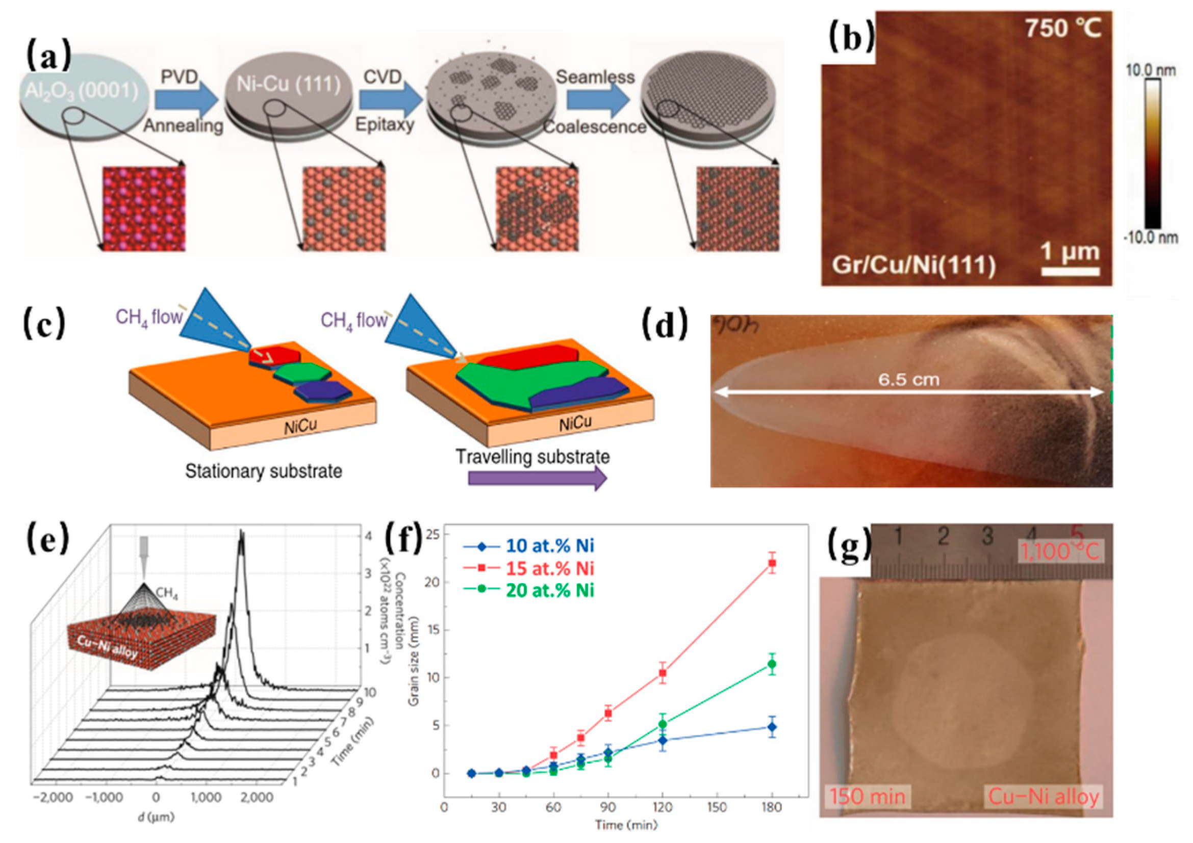
Figure 2.
Synthesis of multilayer graphene on Cu-Ni alloy. (a) illustration of bilayer graphene grown on Cu-Ni alloy, the enlarge figure shows the structure of bilayer graphene; (b) optical image of uniform bilayer graphene on SiO2 (300 nm)/Si substrate; (c) bright field low energy electron microscopy (BF LEEM) image of uniform bilayer graphene and corresponding diffraction patterns (shown in the inset) [33]; (d) Raman spectra of graphene with different thickness formed by changing growth temperature and cooling rate; (e,f) AFM height images of graphene transferred onto a 285 nm SiO2/Si substrate, the dashed lines illustrate the hexagonal multilayer islands; (g,h) height profiles from the indicated “white” location shown in (e,f), respectively [34].

Figure 3.
Synthesis of hexagonal boron nitride (h-BN) on various binary alloys. (a) illustration of single crystal h-BN grown on Cu-Ni alloy; (b) scanning electron microscope (SEM) image of as-grown h-BN domains on Cu-Ni alloy [35]; (c) phase diagram of Cu-Si binary alloy; (d) SEM image of h-BN domains on Cu-Si alloy [36]; (e) schematic of catalyst system composed of Fe/SiO2/Si; (f) SEM image of a large, tooth-edged h-BN domain grown on Fe (1000 nm)/SiO2 (300 nm)/Si substrates. [37]; (g) schematic of multilayer h-BN grown on a Ni−Fe catalyst, the enlarge figure shows the diffusion path of B and N atoms; (h) cross-sectional transmission electron microscopy (TEM) image of the as-grown h-BN on Ni−Fe/spinel (100) [38]; (i) illustration of multilayer h-BN grown on Fe2B alloy by using N2 as a precursor; (j) SEM image of h-BN films grown on Fe–B alloy. A corresponding AFM image with height profile was displayed in the inset; (k) high resolution (HR) TEM image of multilayer h-BN, the inset displays the selected area electron diffraction (SAED) pattern; (l) typical TEM image of as-grown multilayer h-BN [39].
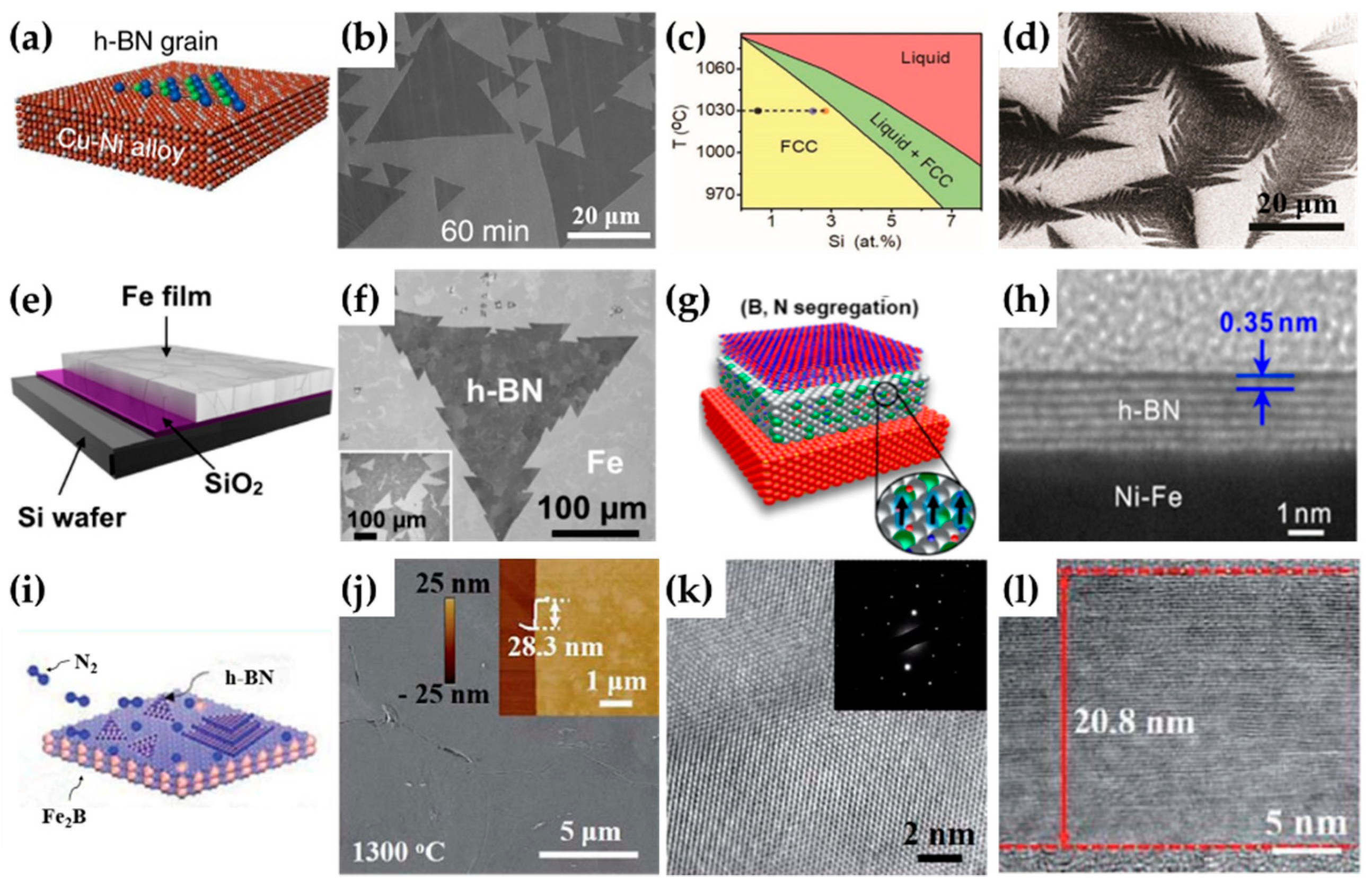
Figure 4.
Synthesis of MXn on various binary alloys. (a) schematic of the synthesis process of perfect α-Mo2C crystals (shown in the inset) through vapor-solid reaction [46]; (b) typical optical image of ultrathin α-Mo2C crystals on a Cu/Mo substrate; (c) scanning transmission electron microscopy (STEM) image of α-Mo2C. Note that the C atoms (indicated by red circle) are located at the center of six Mo atoms (indicated by green circles), forming an orthorhombic structure [43]; (d) schematic overview of the synthesis process of MXn on Au-M alloy; (e) SEM image of an individual MoS2 domain on Au-Mo catalyst; (f) low energy electron diffraction (LEED) pattern of as-grown MoS2 on Au-Mo alloy [47]; (g) AFM image taken at the edge of transferred MoS2 atomic layers; (h) Fourier-filtered image of high-resolution TEM (HRTEM) of MoS2 [48].

Figure 5.
Assembling of graphene/h-BN heterostructures on binary alloy. (a) illustration of the formation of graphene/h-BN in-plane heterostructure on the Cu-Ni alloy, the red line shows the growth path of carbon atoms; (b) typical SEM image of as-grown graphene/h-BN in-plane heterostructure; (c) survey auger electron spectroscopy (AES) spectra taken in the dotted areas shown in (b). [65]; (d) illustration of the formation of h-BN/Graphene stacked heterostructures after the above-mentioned in-plane heterostructure obtained; (e) the SEM image of as-grown stacked heterostructures; (f) survey AES spectra taken in the dotted areas shown in (e) [66].
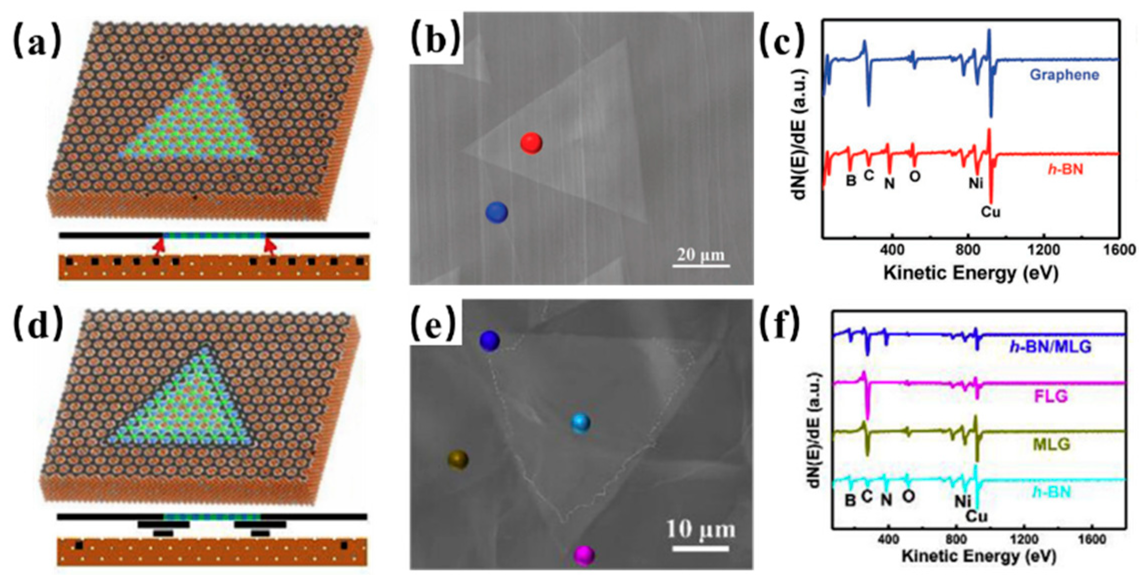
Figure 6.
Assembling of other 2D heterostructures on binary alloy. (a) schematic for the twinned growth of ReS2/WS2. Au is chosen as the growth substrate and W-Re alloy foil serves as the support substrate; (b) SEM image of the triangular ReS2/WS2 vertical crystalline heterostructures. A ReS2/WS2 crystal with grain size up to 600 mm2 is indicated; (c) Fast Fourier transform (FFT) patterns of the ReS2/WS2 heterostructures. The inset shows the two patterns of ReS2 (green) and WS2 (purple) with a rotation angle to be about 5.6° [69]; (d) schematic of the synthesis process for transition metal dichalcogenides/h-BN (TMDCs/h-BN) heterostructures on the Ni-Ga alloy; (e) SEM image of the directly grown single-crystal MoS2 on h-BN; (f) TEM characterizations of MoS2/h-BN heterostructures. The inset shows the corresponding SAED pattern [70].

Table 1.
Summary of the chemical vapor deposition (CVD)-grown 2D materials and heterostructures on rational designed alloys.
Table 1.
Summary of the chemical vapor deposition (CVD)-grown 2D materials and heterostructures on rational designed alloys.
| Substrate | CVD Route | Material Obtained | Precursors | Growth Temp. (°C) | Growth Time (min) | Domain Size | Thickness | Year | Ref. |
|---|---|---|---|---|---|---|---|---|---|
| Cu/Ni | APCVD | graphene | CH4 | 750 | 60 | >2 µm | Monolayer | 2019 | [30] |
| Cu/Ni | APCVD | graphene | CH4/C2H6 | 1100 | 45 | -- | Monolayer | 2018 | [31] |
| Cu/Ni | APCVD | graphene | CH4 | 1050–1100 | 150 | ~4 cm | Monolayer | 2016 | [32] |
| Cu/Ni | APCVD | graphene | CH4 | 1075 | 30 | -- | Bilayer | 2016 | [33] |
| Cu/Ni | LPCVD (cold-wall) | graphene | CH4 | 930–1030 | 3 | -- | Monolayer-19 nm | 2011 | [34] |
| Au/Ni | LPCVD (cold-wall) | graphene | C2H2 | 450 | 7 | >15 µm | Monolayer | 2011 | [73] |
| Co/Cu | APCVD | graphene | CH4 | 850–1050 | 5 | -- | 1–4 layers | 2013 | [74] |
| Mo/Ni | APCVD | graphene | CH4 | 1000 | 25 | 120 nm | Monolayer | 2013 | [75] |
| Cu/Ni | LPCVD | h-BN | H3BNH3 | 1050–1090 | 60 | 70–90 µm | Monolayer | 2015 | [35] |
| Cu/Si | LPCVD | h-BN | H2BNH2 | 1035 | 60 | 0.25 mm | Monolayer | 2019 | [36] |
| Fe/Si | UHV-CVD (cold-wall) | h-BN | (HBNH)3 | 940 | 5 | 0.33 mm | Monolayer | 2015 | [37] |
| Fe/Ni | LPCVD | h-BN | B3H6N3 | 1100 | 30 | -- | 2−5 nm | 2018 | [38] |
| Fe2B | APCVD | h-BN | N2 | 1300 | 60 | -- | ~30 nm | 2019 | [39] |
| Cu/Mo | APCVD | Mo2C | CH4 | 1092 | 3 | 10 nm | ∼3 nm | 2015 | [43] |
| Cu/Mo | APCVD | Mo2C/Gr | CH4 | 1100 | 60 | 100 µm | 170–250 nm | 2017 | [44] |
| Au/Mo | APCVD | MoS2 | H2S | 300 | 30 | -- | 1.66 nm | 2014 | [48] |
© 2020 by the authors. Licensee MDPI, Basel, Switzerland. This article is an open access article distributed under the terms and conditions of the Creative Commons Attribution (CC BY) license (http://creativecommons.org/licenses/by/4.0/).
Share and Cite
MDPI and ACS Style
Zhu, H.; Zhang, C.; Zhang, X.; Shi, Z.; Wu, T.; Yu, G. Overview of Rational Design of Binary Alloy for the Synthesis of Two-Dimensional Materials. Surfaces 2020, 3, 26-39. https://doi.org/10.3390/surfaces3010003
AMA Style
Zhu H, Zhang C, Zhang X, Shi Z, Wu T, Yu G. Overview of Rational Design of Binary Alloy for the Synthesis of Two-Dimensional Materials. Surfaces. 2020; 3(1):26-39. https://doi.org/10.3390/surfaces3010003
Chicago/Turabian StyleZhu, Hongyan, Chao Zhang, Xuefu Zhang, Zhiyuan Shi, Tianru Wu, and Guanghui Yu. 2020. "Overview of Rational Design of Binary Alloy for the Synthesis of Two-Dimensional Materials" Surfaces 3, no. 1: 26-39. https://doi.org/10.3390/surfaces3010003