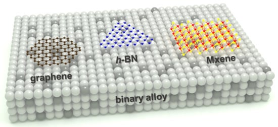
Overview of Rational Design of Binary Alloy for the Synthesis of Two-Dimensional Materials

 ,
,
Abstract
:
1. Introduction
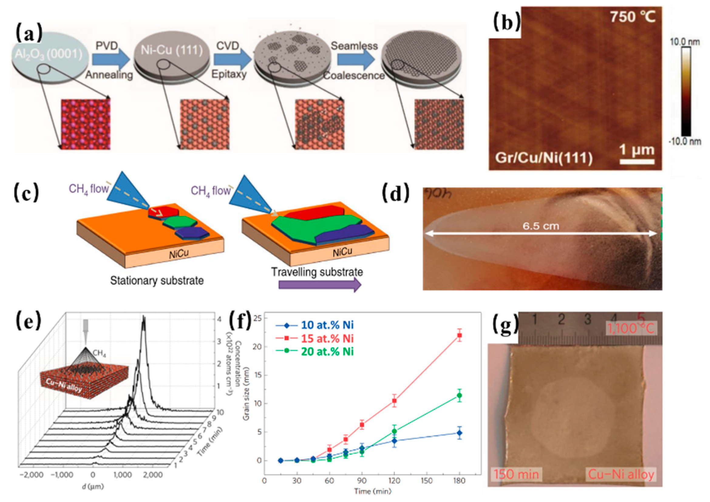
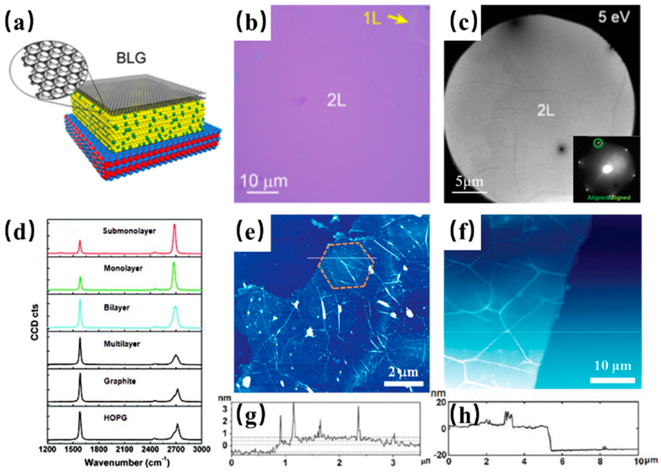
2. Synthesis of Graphene on Cu-Ni Alloy
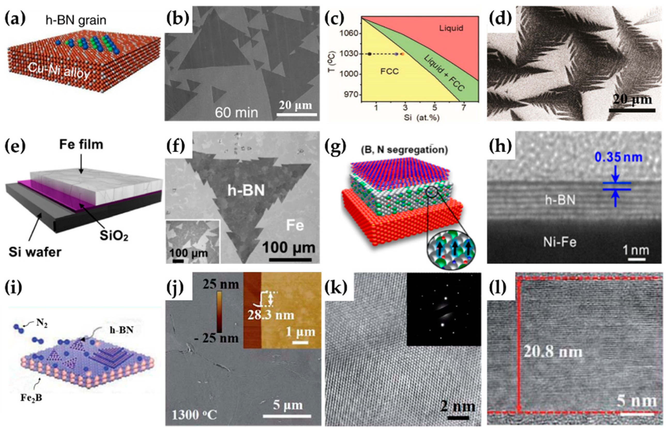
3. Synthesis of h-BN on Binary Alloy
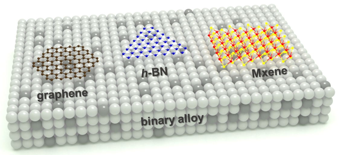
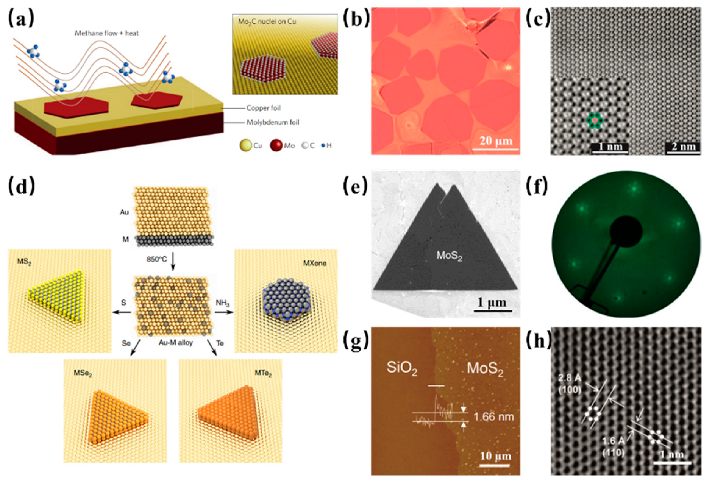
4. Other 2D Materials Grown on Binary Alloy
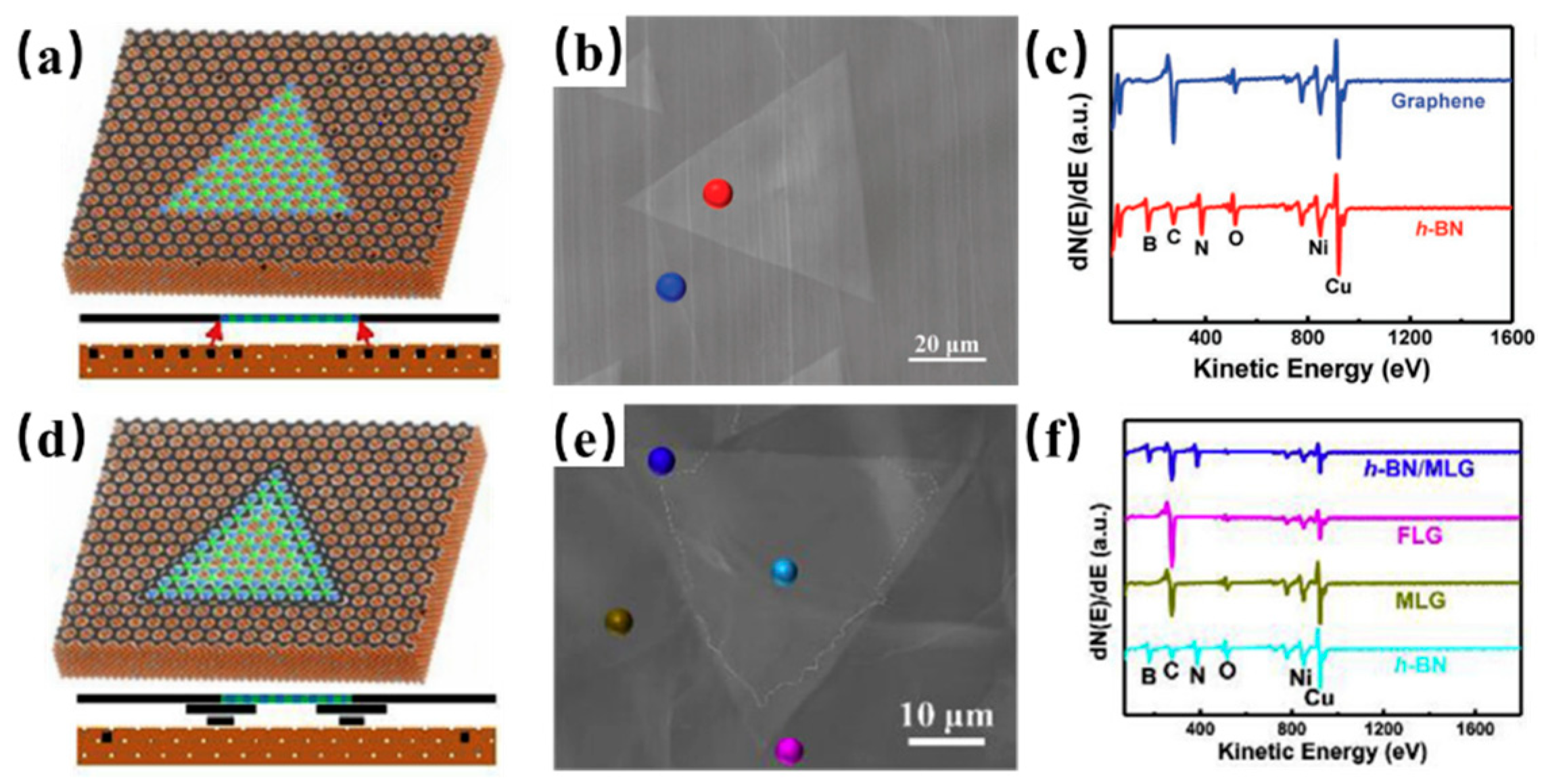
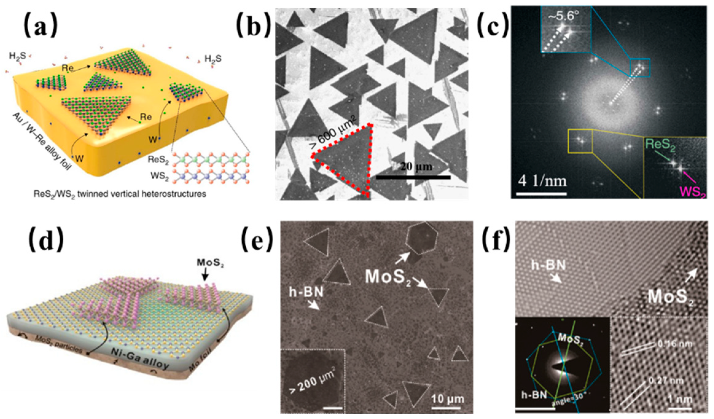
5. 2D Heterostructures Assembled on a Binary Alloy
6. Conclusions
Author Contributions
Funding
Conflicts of Interest
Abbreviations
| 2D | Two-dimensional |
| h-BN | Hexagonal boron nitride |
| TMC | Transition metal carbide |
| TMDCs | Transition metal dichalcogenides |
| CVD | Chemical vapor deposition |
| AFM | Atomic force microscopy |
| RMS | Root mean square |
| SIMS | Secondary ion mass spectrometry |
| BF | Bright field |
| LEEM | Low energy electron microscopy |
| LPCVD | Low-pressure chemical vapor deposition |
| FCC | Face-center cubic |
| SEM | Scanning electron microscope |
| TEM | Transmission electron microscopy |
| HRTEM | High resolution transmission electron microscopy |
| SAED | Selected area electron diffraction |
| STEM | Scanning transmission electron microscopy |
| LEED | Low energy electron diffraction |
| FFT | Fast Fourier transform |
| AES | Auger electron spectroscopy |
| Gr/h-BN | Graphene/hexagonal boron nitride heterostructure |
| APCVD | Atmospheric pressure chemical vapor deposition |
References
- Novoselov, K.S.; Geim, A.K.; Morozov, S.V.; Jiang, D.; Zhang, Y.; Dubonos, S.V.; Grigorieva, I.V.; Firsov, A.A. Electric field effect in atomically thin carbon films. Science 2004, 306, 666–669. [Google Scholar] [CrossRef] [PubMed] [Green Version]
- Lien, D.-H.; Kang, J.S.; Amani, M.; Chen, K.; Tosun, M.; Wang, H.-P.; Roy, T.; Eggleston, M.S.; Wu, M.C.; Dubey, M.; et al. Engineering Light Outcoupling in 2D Materials. Nano Lett. 2015, 15, 1356–1361. [Google Scholar] [CrossRef] [PubMed]
- Zhang, X.; Hou, L.; Ciesielski, A.; Samori, P. 2D Materials Beyond Graphene for High-Performance Energy Storage Applications. Adv. Energy Mater. 2016, 6, 1600671. [Google Scholar] [CrossRef] [Green Version]
- Xu, X.; Chen, J.; Li, B. Phonon thermal conduction in novel 2D materials. J. Phys. Condens. Matter 2016, 28, 48. [Google Scholar] [CrossRef]
- Wang, H.; Huang, X.; Lin, J.; Cui, J.; Chen, Y.; Zhu, C.; Liu, F.; Zeng, Q.; Zhou, J.; Yu, P.; et al. High-quality monolayer superconductor NbSe2 grown by chemical vapour deposition. Nat. Commun. 2017, 8, 394. [Google Scholar] [CrossRef] [PubMed]
- Wang, L.; Zhu, Y.; Wang, J.-Q.; Liu, F.; Huang, J.; Meng, X.; Basset, J.-M.; Han, Y.; Xiao, F.-S. Two-dimensional gold nanostructures with high activity for selective oxidation of carbon-hydrogen bonds. Nat. Commun. 2015, 6, 6957. [Google Scholar] [CrossRef] [PubMed] [Green Version]
- Lee, Y.-H.; Zhang, X.-Q.; Zhang, W.; Chang, M.-T.; Lin, C.-T.; Chang, K.-D.; Yu, Y.-C.; Wang, J.T.-W.; Chang, C.-S.; Li, L.-J.; et al. Synthesis of Large-Area MoS2 Atomic Layers with Chemical Vapor Deposition. Adv. Mater. 2012, 24, 2320–2325. [Google Scholar] [CrossRef] [Green Version]
- Smith, J.B.; Hagaman, D.; Ji, H.-F. Growth of 2D black phosphorus film from chemical vapor deposition. Nanotechnology 2016, 27, 21. [Google Scholar] [CrossRef]
- Shi, Y.; Hamsen, C.; Jia, X.; Kim, K.K.; Reina, A.; Hofmann, M.; Hsu, A.L.; Zhang, K.; Li, H.; Juang, Z.-Y.; et al. Synthesis of Few-Layer Hexagonal Boron Nitride Thin Film by Chemical Vapor Deposition. Nano Lett. 2010, 10, 4134–4139. [Google Scholar] [CrossRef]
- Zhuang, A.; Li, J.-J.; Wang, Y.-C.; Wen, X.; Lin, Y.; Xiang, B.; Wang, X.; Zeng, J. Screw-Dislocation-Driven Bidirectional Spiral Growth of Bi2Se3 Nanoplates. Angew. Chem. Int. Ed. 2014, 53, 6425–6429. [Google Scholar] [CrossRef]
- Geim, A.K.; Grigorieva, I.V. Van der Waals heterostructures. Nature 2013, 499, 419–425. [Google Scholar] [CrossRef] [PubMed]
- Iannaccone, G.; Bonaccorso, F.; Colombo, L.; Fiori, G. Quantum engineering of transistors based on 2D materials heterostructures. Nat. Nanotechnol. 2018, 13, 183–191. [Google Scholar] [CrossRef] [PubMed]
- Chen, K.; Wan, X.; Wen, J.; Xie, W.; Kang, Z.; Zeng, X.; Chen, H.; Xu, J.-B. Electronic Properties of MoS2-WS2 Heterostructures Synthesized with Two-Step Lateral Epitaxial Strategy. ACS Nano 2015, 9, 9868–9876. [Google Scholar] [CrossRef] [PubMed]
- Novoselov, K.S.; Fal’ko, V.I.; Colombo, L.; Gellert, P.R.; Schwab, M.G.; Kim, K. A roadmap for graphene. Nature 2012, 490, 192–200. [Google Scholar] [CrossRef] [PubMed]
- Tan, L.; Zeng, M.; Zhang, T.; Fu, L. Design of catalytic substrates for uniform graphene films: From solid-metal to liquid-metal. Nanoscale 2015, 7, 9105–9121. [Google Scholar] [CrossRef] [PubMed]
- Li, X.; Cai, W.; An, J.; Kim, S.; Nah, J.; Yang, D.; Piner, R.; Velamakanni, A.; Jung, I.; Tutuc, E.; et al. Large-Area Synthesis of High-Quality and Uniform Graphene Films on Copper Foils. Science 2009, 324, 1312–1314. [Google Scholar] [CrossRef] [Green Version]
- Wang, L.; Wu, B.; Jiang, L.; Chen, J.; Li, Y.; Guo, W.; Hu, P.; Liu, Y. Growth and Etching of Monolayer Hexagonal Boron Nitride. Adv. Mater. 2015, 27, 4858–4864. [Google Scholar] [CrossRef]
- Kim, K.S.; Zhao, Y.; Jang, H.; Lee, S.Y.; Kim, J.M.; Kim, K.S.; Ahn, J.-H.; Kim, P.; Choi, J.-Y.; Hong, B.H. Large-scale pattern growth of graphene films for stretchable transparent electrodes. Nature 2009, 457, 706–710. [Google Scholar] [CrossRef]
- Gao, L.; Ren, W.; Xu, H.; Jin, L.; Wang, Z.; Ma, T.; Ma, L.-P.; Zhang, Z.; Fu, Q.; Peng, L.-M.; et al. Repeated growth and bubbling transfer of graphene with millimetre-size single-crystal grains using platinum. Nat. Commun. 2012, 3, 699. [Google Scholar] [CrossRef]
- Sutter, E.; Albrecht, P.; Sutter, P. Graphene growth on polycrystalline Ru thin films. Appl. Phys. Lett. 2009, 95, 133109. [Google Scholar] [CrossRef]
- Nie, S.; Bartelt, N.C.; Wofford, J.M.; Dubon, O.D.; McCarty, K.F.; Thuermer, K. Scanning tunneling microscopy study of graphene on Au(111): Growth mechanisms and substrate interactions. Phys. Rev. B 2012, 85, 205406. [Google Scholar] [CrossRef] [Green Version]
- An, H.; Lee, W.-J.; Jung, J. Graphene synthesis on Fe foil using thermal CVD. Curr. Appl. Phys. 2011, 11, S81–S85. [Google Scholar] [CrossRef]
- Kim, E.; An, H.; Jang, H.; Cho, W.-J.; Lee, N.; Lee, W.-G.; Jung, J. Growth of Few-Layer Graphene on a Thin Cobalt Film on a Si/SiO2 Substrate. Chem. Vap. Depos. 2011, 17, 9–14. [Google Scholar] [CrossRef]
- Ago, H.; Ogawa, Y.; Tsuji, M.; Mizuno, S.; Hibino, H. Catalytic Growth of Graphene: Toward Large-Area Single-Crystalline Graphene. J. Phys. Chem. Lett. 2012, 3, 2228–2236. [Google Scholar] [CrossRef] [PubMed]
- Patera, L.L.; Africh, C.; Weatherup, R.S.; Blume, R.; Bhardwaj, S.; Castellarin-Cudia, C.; Knop-Gericke, A.; Schloegl, R.; Comelli, G.; Hofmann, S.; et al. In Situ Observations of the Atomistic Mechanisms of Ni Catalyzed Low Temperature Graphene Growth. ACS Nano 2013, 7, 7901–7912. [Google Scholar] [CrossRef] [Green Version]
- Wang, H.; Wang, G.; Bao, P.; Yang, S.; Zhu, W.; Xie, X.; Zhang, W.-J. Controllable Synthesis of Submillimeter Single-Crystal Monolayer Graphene Domains on Copper Foils by Suppressing Nucleation. J. Am. Chem. Soc. 2012, 134, 3627–3630. [Google Scholar] [CrossRef]
- Yan, Z.; Lin, J.; Peng, Z.; Sun, Z.; Zhu, Y.; Li, L.; Xiang, C.; Samuel, E.L.; Kittrell, C.; Tour, J.M. Toward the Synthesis of Wafer-Scale Single-Crystal Graphene on Copper Foils. ACS Nano 2012, 6, 9110–9117. [Google Scholar] [CrossRef]
- Yu, Q.; Lian, J.; Siriponglert, S.; Li, H.; Chen, Y.P.; Pei, S.-S. Graphene segregated on Ni surfaces and transferred to insulators. Appl. Phys. Lett. 2008, 93, 113103. [Google Scholar] [CrossRef] [Green Version]
- Liu, Y.; Wu, T.; Yin, Y.; Zhang, X.; Yu, Q.; Searles, D.J.; Ding, F.; Yuan, Q.; Xie, X. How Low Nucleation Density of Graphene on Cu-Ni Alloy is Achieved. Adv. Sci. 2018, 5, 1700961. [Google Scholar] [CrossRef]
- Zhang, X.; Wu, T.; Jiang, Q.; Wang, H.; Zhu, H.; Chen, Z.; Jiang, R.; Niu, T.; Li, Z.; Zhang, Y.; et al. Epitaxial Growth of 6 in. Single-Crystalline Graphene on a Cu/Ni (111) Film at 750 °C via Chemical Vapor Deposition. Small 2019, 15, 1805395. [Google Scholar] [CrossRef]
- Vlassiouk, I.V.; Stehle, Y.; Pudasaini, P.R.; Unocic, R.R.; Rack, P.D.; Baddorf, A.P.; Ivanov, I.N.; Lavrik, N.V.; List, F.; Gupta, N.; et al. Evolutionary selection growth of two-dimensional materials on polycrystalline substrates. Nat. Mater. 2018, 17, 318. [Google Scholar] [CrossRef]
- Wu, T.; Zhang, X.; Yuan, Q.; Xue, J.; Lu, G.; Liu, Z.; Wang, H.; Wang, H.; Ding, F.; Yu, Q.; et al. Fast growth of inch-sized single-crystalline graphene from a controlled single nucleus on Cu-Ni alloys. Nat. Mater. 2016, 15, 43. [Google Scholar] [CrossRef] [PubMed]
- Takesaki, Y.; Kawahara, K.; Hibino, H.; Okada, S.; Tsuji, M.; Ago, H. Highly Uniform Bilayer Graphene on Epitaxial Cu-Ni(111) Alloy. Chem. Mater. 2016, 28, 4583–4592. [Google Scholar] [CrossRef]
- Chen, S.; Cai, W.; Piner, R.D.; Suk, J.W.; Wu, Y.; Ren, Y.; Kang, J.; Ruoff, R.S. Synthesis and Characterization of Large-Area Graphene and Graphite Films on Commercial Cu-Ni Alloy Foils. Nano Lett. 2011, 11, 3519–3525. [Google Scholar] [CrossRef] [PubMed]
- Lu, G.; Wu, T.; Yuan, Q.; Wang, H.; Wang, H.; Ding, F.; Xie, X.; Jiang, M. Synthesis of large single-crystal hexagonal boron nitride grains on Cu-Ni alloy. Nat. Commun. 2015, 6, 6160. [Google Scholar] [CrossRef] [PubMed]
- Li, J.; Hu, Z.; Yi, Y.; Yu, M.; Li, X.; Zhou, J.; Yin, J.; Wu, S.; Guo, W. Hexagonal Boron Nitride Growth on Cu-Si Alloy: Morphologies and Large Domains. Small 2019, 15, 1805188. [Google Scholar] [CrossRef] [PubMed]
- Caneva, S.; Weatherup, R.S.; Bayer, B.C.; Brennan, B.; Spencer, S.J.; Mingard, K.; Cabrero-Vilatela, A.; Baehtz, C.; Pollard, A.J.; Hofmann, S. Nucleation Control for Large, Single Crystalline Domains of Mono layer Hexagonal Boron Nitride via Si-Doped Fe Catalysts. Nano Lett. 2015, 15, 1867–1875. [Google Scholar] [CrossRef]
- Uchida, Y.; Nakandakari, S.; Kawahara, K.; Yamasaki, S.; Mitsuhara, M.; Ago, H. Controlled Growth of Large-Area Uniform Multilayer Hexagonal Boron Nitride as an Effective 2D Substrate. ACS Nano 2018, 12, 6236–6244. [Google Scholar] [CrossRef]
- Shi, Z.; Lu, G.; Yang, P.; Wu, T.; Yin, W.; Zhang, C.; Jiang, R.; Xie, X. Controlled synthesis of uniform multilayer hexagonal boron nitride films on Fe2B alloy. RSC Adv. 2019, 9, 10155–10158. [Google Scholar] [CrossRef] [Green Version]
- Butler, S.Z.; Hollen, S.M.; Cao, L.; Cui, Y.; Gupta, J.A.; Gutierrez, H.R.; Heinz, T.F.; Hong, S.S.; Huang, J.; Ismach, A.F.; et al. Progress, Challenges, and Opportunities in Two-Dimensional Materials Beyond Graphene. ACS Nano 2013, 7, 2898–2926. [Google Scholar] [CrossRef]
- Zhong, Y.; Xia, X.; Shi, F.; Zhan, J.; Tu, J.; Fan, H.J. Transition Metal Carbides and Nitrides in Energy Storage and Conversion. Adv. Sci. 2016, 3, 1500286. [Google Scholar] [CrossRef]
- Hantanasirisakul, K.; Gogotsi, Y. Electronic and Optical Properties of 2D Transition Metal Carbides and Nitrides (MXenes). Adv. Mater. 2018, 30, 1804779. [Google Scholar] [CrossRef]
- Xu, C.; Wang, L.; Liu, Z.; Chen, L.; Guo, J.; Kang, N.; Ma, X.-L.; Cheng, H.-M.; Ren, W. Large-area high-quality 2D ultrathin Mo2C superconducting crystals. Nat. Mater. 2015, 14, 1135. [Google Scholar] [CrossRef]
- Geng, D.; Zhao, X.; Chen, Z.; Sun, W.; Fu, W.; Chen, J.; Liu, W.; Zhou, W.; Loh, K.P. Direct Synthesis of Large-Area 2D Mo2C on In Situ Grown Graphene. Adv. Mater. 2017, 29, 1700072. [Google Scholar] [CrossRef]
- Wang, Z.; Kochat, V.; Pandey, P.; Kashyap, S.; Chattopadhyay, S.; Samanta, A.; Sarkar, S.; Manimunda, P.; Zhang, X.; Asif, S.; et al. Metal Immiscibility Route to Synthesis of Ultrathin Carbides, Borides, and Nitrides. Adv. Mater. 2017, 29, 1700364. [Google Scholar] [CrossRef]
- Gogotsi, Y. Chemical Vapour Deposition Transition metal carbides go 2D. Nat. Mater. 2015, 14, 1079–1080. [Google Scholar] [CrossRef]
- Shivayogimath, A.; Thomsen, J.D.; Mackenzie, D.M.A.; Geisler, M.; Stan, R.-M.; Holt, A.J.; Bianchi, M.; Crovetto, A.; Whelan, P.R.; Carvalho, A.; et al. A universal approach for the synthesis of two-dimensional binary compounds. Nat. Commun. 2019, 10, 2957. [Google Scholar] [CrossRef] [Green Version]
- Song, I.; Park, C.; Hong, M.; Baik, J.; Shin, H.-J.; Choi, H.C. Patternable Large-Scale Molybdenium Disulfide Atomic Layers Grown by Gold-Assisted Chemical Vapor Deposition. Angew. Chem. Int. Ed. 2014, 53, 1266–1269. [Google Scholar] [CrossRef] [PubMed]
- Fleurence, A.; Gill, T.G.; Friedlein, R.; Sadowski, J.T.; Aoyagi, K.; Copel, M.; Tromp, R.M.; Hirjibehedin, C.F.; Yamada-Takamura, Y. Single-domain epitaxial silicene on diboride thin films. Appl. Phys. Lett. 2016, 108, 151902. [Google Scholar] [CrossRef] [Green Version]
- Fleurence, A.; Friedlein, R.; Ozaki, T.; Kawai, H.; Wang, Y.; Yamada-Takamura, Y. Experimental Evidence for Epitaxial Silicene on Diboride Thin Films. Phys. Rev. Lett. 2012, 108, 245501. [Google Scholar] [CrossRef] [PubMed]
- Aizawa, T.; Suehara, S.; Otani, S. Silicene on Zirconium Carbide (111). J. Phys. Chem. C 2014, 118, 23049–23057. [Google Scholar] [CrossRef]
- Bampoulis, P.; Zhang, L.; Safaei, A.; van Gastel, R.; Poelsema, B.; Zandvliet, H.J.W. Germanene termination of Ge2Pt crystals on Ge (110). J. Phys. Condens. Matter 2014, 26, 442001. [Google Scholar] [CrossRef] [PubMed] [Green Version]
- Dong, F.; Xiong, T.; Sun, Y.; Zhang, Y.; Zhou, Y. Controlling interfacial contact and exposed facets for enhancing photocatalysis via 2D-2D heterostructures. Chem. Commun. 2015, 51, 8249–8252. [Google Scholar] [CrossRef] [PubMed]
- Wilson, N.R.; Nguyen, P.V.; Seyler, K.; Rivera, P.; Marsden, A.J.; Laker, Z.P.L.; Constantinescu, G.C.; Kandyba, V.; Barinov, A.; Hine, N.D.M.; et al. Determination of band offsets, hybridization, and exciton binding in 2D semiconductor heterostructures. Sci. Adv. 2017, 3, e1601832. [Google Scholar] [CrossRef] [PubMed] [Green Version]
- Wu, Z.-S.; Zheng, Y.; Zheng, S.; Wang, S.; Sun, C.; Parvez, K.; Ikeda, T.; Bao, X.; Muellen, K.; Feng, X. Stacked-Layer Heterostructure Films of 2D Thiophene Nanosheets and Graphene for High-Rate All-Solid-State Pseudocapacitors with Enhanced Volumetric Capacitance. Adv. Mater. 2017, 29, 1602960. [Google Scholar] [CrossRef]
- Dean, C.R.; Young, A.F.; Meric, I.; Lee, C.; Wang, L.; Sorgenfrei, S.; Watanabe, K.; Taniguchi, T.; Kim, P.; Shepard, K.L.; et al. Boron nitride substrates for high-quality graphene electronics. Nat. Nanotechnol. 2010, 5, 722–726. [Google Scholar] [CrossRef]
- Tang, S.; Wang, H.; Wang, H.S.; Sun, Q.; Zhang, X.; Cong, C.; Xie, H.; Liu, X.; Zhou, X.; Huang, F.; et al. Silane-catalysed fast growth of large single-crystalline graphene on hexagonal boron nitride. Nat. Commun. 2015, 6, 6499. [Google Scholar] [CrossRef]
- Wang, J.; Yao, Q.; Huang, C.-W.; Zou, X.; Liao, L.; Chen, S.; Fan, Z.; Zhang, K.; Wu, W.; Xiao, X.; et al. High Mobility MoS2 Transistor with Low Schottky Barrier Contact by Using Atomic Thick h-BN as a Tunneling Layer. Adv. Mater. 2016, 28, 8302–8308. [Google Scholar] [CrossRef]
- Wang, M.; Jang, S.K.; Jang, W.-J.; Kim, M.; Park, S.-Y.; Kim, S.-W.; Kahng, S.-J.; Choi, J.-Y.; Ruoff, R.S.; Song, Y.J.; et al. A Platform for Large-Scale Graphene Electronics-CVD Growth of Single-Layer Graphene on CVD-Grown Hexagonal Boron Nitride. Adv. Mater. 2013, 25, 2746–2752. [Google Scholar] [CrossRef]
- Zhang, C.; Zhao, S.; Jin, C.; Koh, A.L.; Zhou, Y.; Xu, W.; Li, Q.; Xiong, Q.; Peng, H.; Liu, Z. Direct growth of large-area graphene and boron nitride heterostructures by a co-segregation method. Nat. Commun. 2015, 6, 6519. [Google Scholar] [CrossRef] [Green Version]
- Miwa, J.A.; Dendzik, M.; Gronborg, S.S.; Bianchi, M.; Lauritsen, J.V.; Hofmann, P.; Ulstrup, S. Van der Waals Epitaxy of Two-Dimensional MoS2-Graphene Heterostructures in Ultrahigh Vacuum. ACS Nano 2015, 9, 6502–6510. [Google Scholar] [CrossRef] [PubMed]
- Liu, Z.; Ma, L.; Shi, G.; Zhou, W.; Gong, Y.; Lei, S.; Yang, X.; Zhang, J.; Yu, J.; Hackenberg, K.P.; et al. In-plane heterostructures of graphene and hexagonal boron nitride with controlled domain sizes. Nat. Nanotechnol. 2013, 8, 119–124. [Google Scholar] [CrossRef] [PubMed]
- Gong, Y.; Lin, J.; Wang, X.; Shi, G.; Lei, S.; Lin, Z.; Zou, X.; Ye, G.; Vajtai, R.; Yakobson, B.I.; et al. Vertical and in-plane heterostructures from WS2/MoS2 monolayers. Nat. Mater. 2014, 13, 1135–1142. [Google Scholar] [CrossRef] [PubMed] [Green Version]
- Wang, S.; Wang, X.; Warner, J.H. All Chemical Vapor Deposition Growth of MoS2:h-BN Vertical van der Waals Heterostructures. ACS Nano 2015, 9, 5246–5254. [Google Scholar] [CrossRef] [PubMed]
- Lu, G.; Wu, T.; Yang, P.; Yang, Y.; Jin, Z.; Chen, W.; Jia, S.; Wang, H.; Zhang, G.; Sun, J.; et al. Synthesis of High-Quality Graphene and Hexagonal Boron Nitride Monolayer In-Plane Heterostructure on Cu-Ni Alloy. Adv. Sci. 2017, 4, 1700076. [Google Scholar] [CrossRef] [Green Version]
- Lu, G.; Zhang, G.; Sun, J.; Wang, X.; Shi, Z.; Jiang, D.; Wang, H.; Li, A.; Wu, T.; Yu, Q.; et al. Synthesis and stacking sequence characterization of h-BN/graphene heterostructures on Cu-Ni alloy. Carbon 2019, 152, 521–526. [Google Scholar] [CrossRef]
- Cheng, R.; Li, D.; Zhou, H.; Wang, C.; Yin, A.; Jiang, S.; Liu, Y.; Chen, Y.; Huang, Y.; Duan, X. Electroluminescence and Photocurrent Generation from Atomically Sharp WSe2/MoS2 Heterojunction p-n Diodes. Nano Lett. 2014, 14, 5590–5597. [Google Scholar] [CrossRef] [Green Version]
- Komsa, H.-P.; Krasheninnikov, A.V. Electronic structures and optical properties of realistic transition metal dichalcogenide heterostructures from first principles. Phys. Rev. B 2013, 88, 085318. [Google Scholar] [CrossRef] [Green Version]
- Zhang, T.; Jiang, B.; Xu, Z.; Mendes, R.G.; Xiao, Y.; Chen, L.; Fang, L.; Gemming, T.; Chen, S.; Ruemmeli, M.H.; et al. Twinned growth behaviour of two-dimensional materials. Nat. Commun. 2016, 7, 13911. [Google Scholar] [CrossRef]
- Fu, L.; Sun, Y.; Wu, N.; Mendes, R.G.; Chen, L.; Xu, Z.; Zhang, T.; Ruemmeli, M.H.; Rellinghaus, B.; Pohl, D.; et al. Direct Growth of MoS2/h-BN Heterostructures via a Sulfide-Resistant Alloy. ACS Nano 2016, 10, 2063–2070. [Google Scholar] [CrossRef]
- Okada, M.; Sawazaki, T.; Watanabe, K.; Taniguch, T.; Hibino, H.; Shinohara, H.; Kitaura, R. Direct Chemical Vapor Deposition Growth of WS2 Atomic Layers on Hexagonal Boron Nitride. ACS Nano 2014, 8, 8273–8277. [Google Scholar] [CrossRef] [PubMed]
- Zhang, M.; Zhu, Y.; Wang, X.; Feng, Q.; Qiao, S.; Wen, W.; Chen, Y.; Cui, M.; Zhang, J.; Cai, C.; et al. Controlled Synthesis of ZrS2 Mono layer and Few Layers on Hexagonal Boron Nitride. J. Am. Chem. Soc. 2015, 137, 7051–7054. [Google Scholar] [CrossRef] [PubMed]
- Weatherup, R.S.; Bayer, B.C.; Blume, R.; Ducati, C.; Baehtz, C.; Schloegl, R.; Hofmann, S. In Situ Characterization of Alloy Catalysts for Low-Temperature Graphene Growth. Nano Lett. 2011, 11, 4154–4160. [Google Scholar] [CrossRef] [PubMed]
- Lin, T.; Huang, F.; Wan, D.; Bi, H.; Xie, X.; Jiang, M. Self-regulating homogenous growth of high-quality graphene on Co-Cu composite substrate for layer control. Nanoscale 2013, 5, 5847–5853. [Google Scholar] [CrossRef] [PubMed]
- Ruemmeli, M.H.; Zeng, M.; Melkhanova, S.; Gorantla, S.; Bachmatiuk, A.; Fu, L.; Yan, C.; Oswald, S.; Mendes, R.G.; Makarov, D.; et al. Insights into the Early Growth of Homogeneous Single-Layer Graphene over Ni-Mo Binary Substrates. Chem. Mater. 2013, 25, 3880–3887. [Google Scholar] [CrossRef]


| Substrate | CVD Route | Material Obtained | Precursors | Growth Temp. (°C) | Growth Time (min) | Domain Size | Thickness | Year | Ref. |
|---|---|---|---|---|---|---|---|---|---|
| Cu/Ni | APCVD | graphene | CH4 | 750 | 60 | >2 µm | Monolayer | 2019 | [30] |
| Cu/Ni | APCVD | graphene | CH4/C2H6 | 1100 | 45 | -- | Monolayer | 2018 | [31] |
| Cu/Ni | APCVD | graphene | CH4 | 1050–1100 | 150 | ~4 cm | Monolayer | 2016 | [32] |
| Cu/Ni | APCVD | graphene | CH4 | 1075 | 30 | -- | Bilayer | 2016 | [33] |
| Cu/Ni | LPCVD (cold-wall) | graphene | CH4 | 930–1030 | 3 | -- | Monolayer-19 nm | 2011 | [34] |
| Au/Ni | LPCVD (cold-wall) | graphene | C2H2 | 450 | 7 | >15 µm | Monolayer | 2011 | [73] |
| Co/Cu | APCVD | graphene | CH4 | 850–1050 | 5 | -- | 1–4 layers | 2013 | [74] |
| Mo/Ni | APCVD | graphene | CH4 | 1000 | 25 | 120 nm | Monolayer | 2013 | [75] |
| Cu/Ni | LPCVD | h-BN | H3BNH3 | 1050–1090 | 60 | 70–90 µm | Monolayer | 2015 | [35] |
| Cu/Si | LPCVD | h-BN | H2BNH2 | 1035 | 60 | 0.25 mm | Monolayer | 2019 | [36] |
| Fe/Si | UHV-CVD (cold-wall) | h-BN | (HBNH)3 | 940 | 5 | 0.33 mm | Monolayer | 2015 | [37] |
| Fe/Ni | LPCVD | h-BN | B3H6N3 | 1100 | 30 | -- | 2−5 nm | 2018 | [38] |
| Fe2B | APCVD | h-BN | N2 | 1300 | 60 | -- | ~30 nm | 2019 | [39] |
| Cu/Mo | APCVD | Mo2C | CH4 | 1092 | 3 | 10 nm | ∼3 nm | 2015 | [43] |
| Cu/Mo | APCVD | Mo2C/Gr | CH4 | 1100 | 60 | 100 µm | 170–250 nm | 2017 | [44] |
| Au/Mo | APCVD | MoS2 | H2S | 300 | 30 | -- | 1.66 nm | 2014 | [48] |
© 2020 by the authors. Licensee MDPI, Basel, Switzerland. This article is an open access article distributed under the terms and conditions of the Creative Commons Attribution (CC BY) license (http://creativecommons.org/licenses/by/4.0/).
Share and Cite
Zhu, H.; Zhang, C.; Zhang, X.; Shi, Z.; Wu, T.; Yu, G. Overview of Rational Design of Binary Alloy for the Synthesis of Two-Dimensional Materials. Surfaces 2020, 3, 26-39. https://doi.org/10.3390/surfaces3010003
Zhu H, Zhang C, Zhang X, Shi Z, Wu T, Yu G. Overview of Rational Design of Binary Alloy for the Synthesis of Two-Dimensional Materials. Surfaces. 2020; 3(1):26-39. https://doi.org/10.3390/surfaces3010003
Chicago/Turabian StyleZhu, Hongyan, Chao Zhang, Xuefu Zhang, Zhiyuan Shi, Tianru Wu, and Guanghui Yu. 2020. "Overview of Rational Design of Binary Alloy for the Synthesis of Two-Dimensional Materials" Surfaces 3, no. 1: 26-39. https://doi.org/10.3390/surfaces3010003