Interface Behaviour and Work Function Modification of Self-Assembled Monolayers on Sn-Doped In2O3


Abstract
:1. Introduction
2. Experimental
3. Results and Discussion
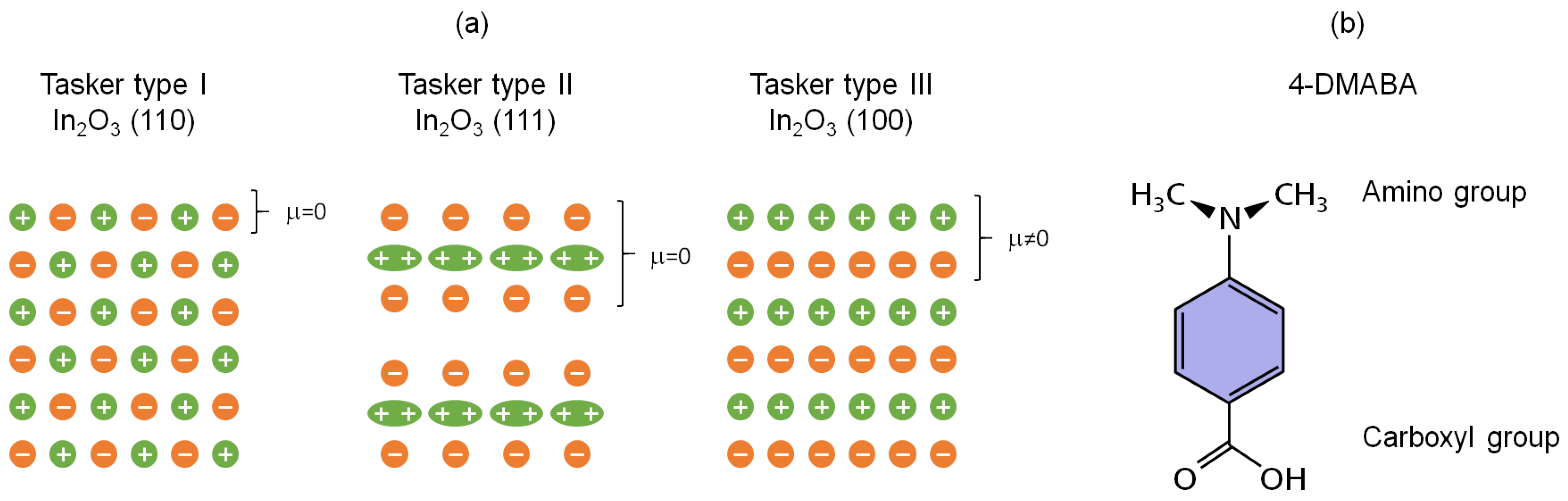
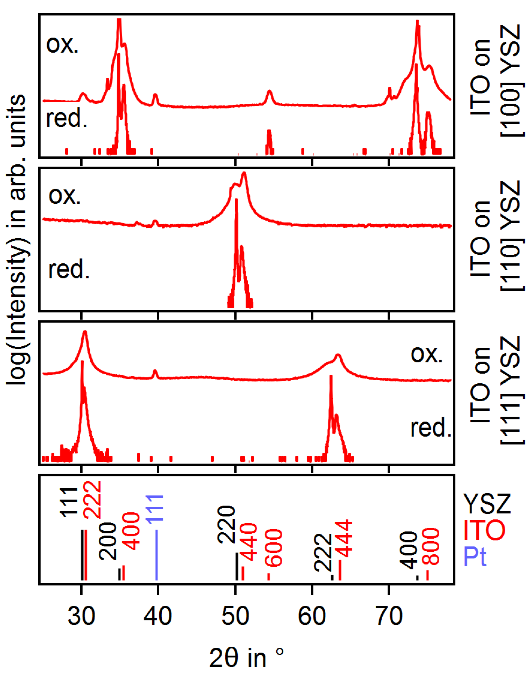
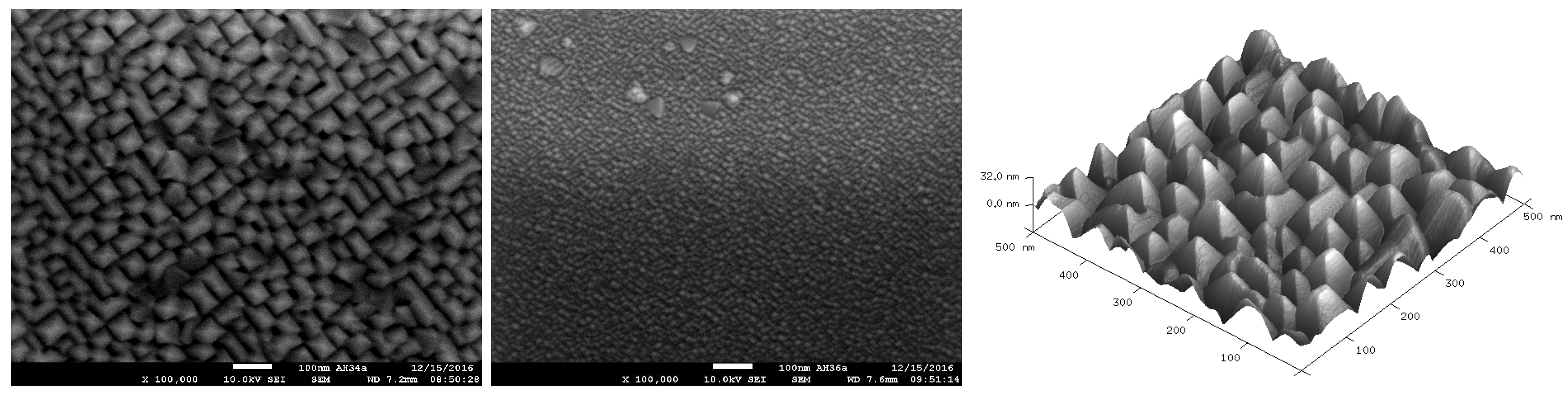
3.1. Oriented ITO Films
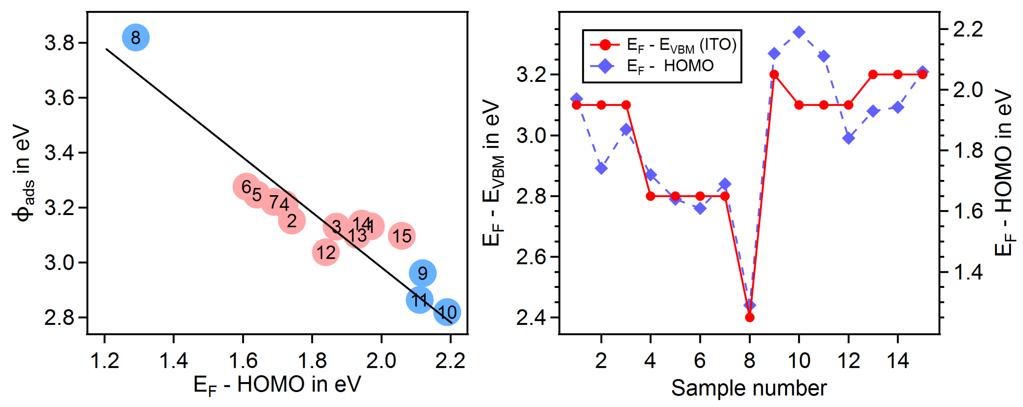
3.2. ITO Surface Potentials
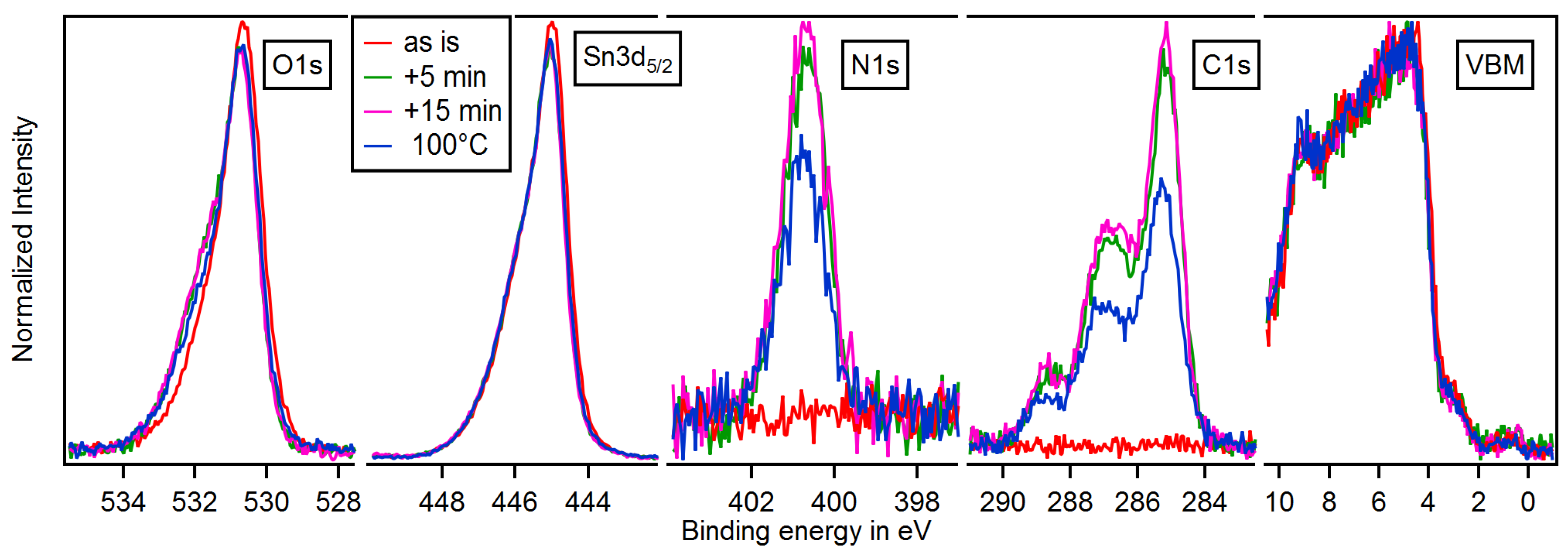
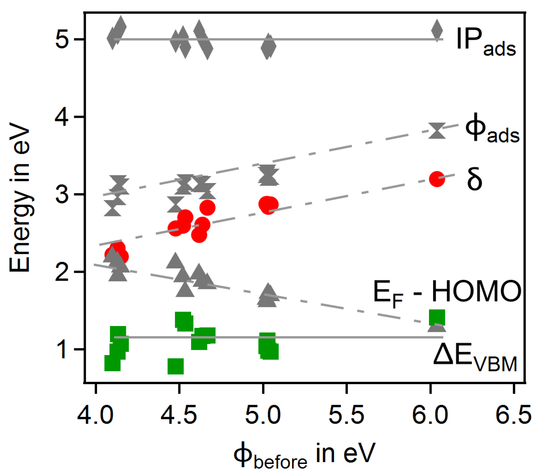
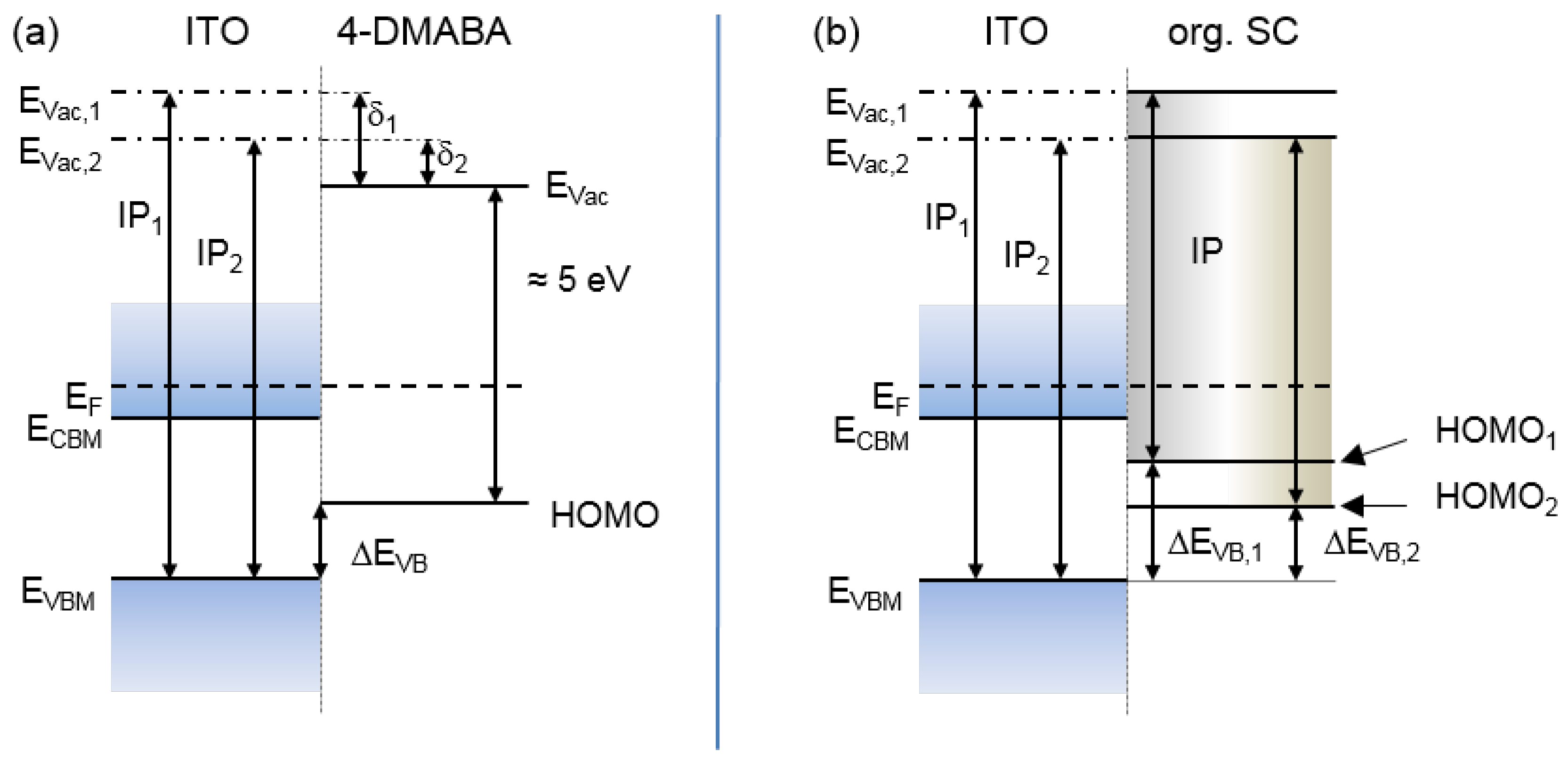
3.3. Adsorption of 4-DMABA
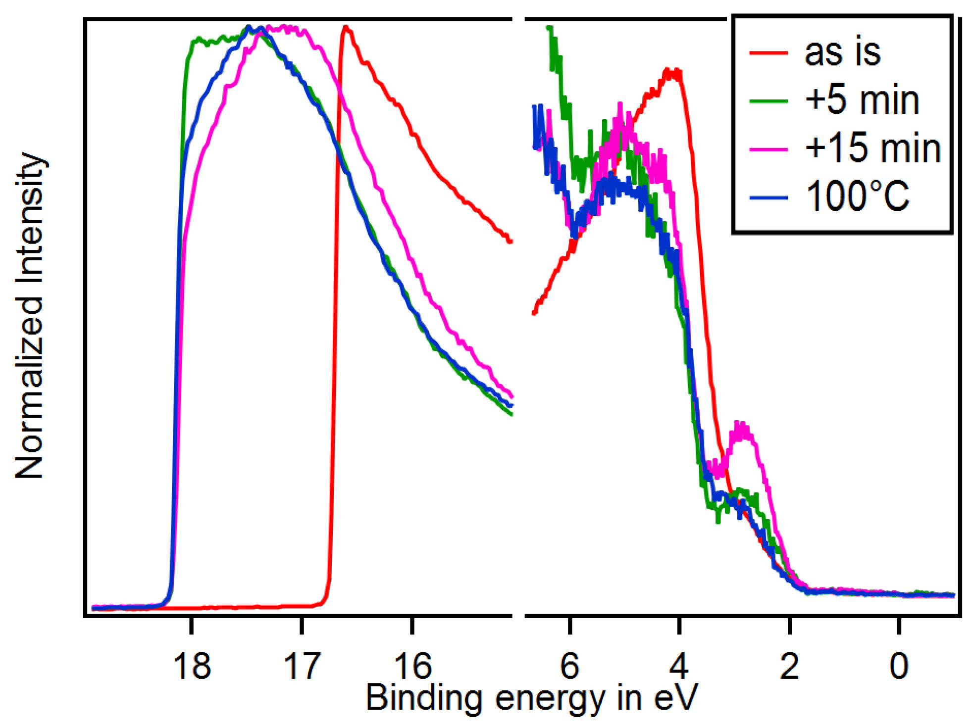
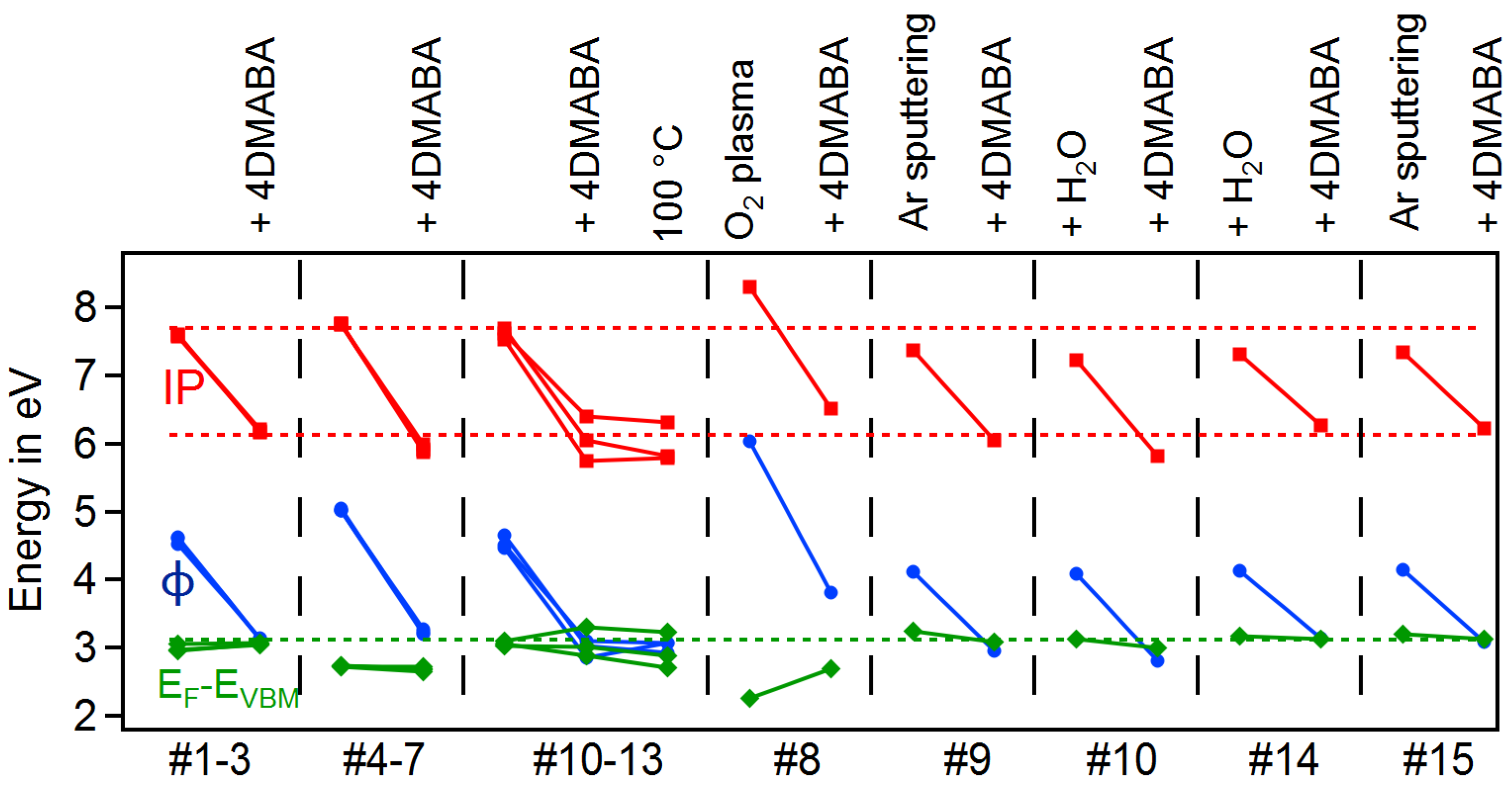
3.4. Dependence on Surface Orientation and Treatment
4. Summary and Conclusions
Author Contributions
Funding
Conflicts of Interest
Abbreviations
| 4-DMABA | 4-(Dimethylamino)benzoic acid |
| ITO | Sn-doped In2O3 |
| YSZ | Y-stabilized zirconia (ZrO:Y) |
| HOMO | higher occupied molecular orbital |
| VBM | valence band maximum |
| SAM | self-assembled monolayer |
| XPS | X-ray photoelectron spectroscopy |
| UPS | ultraviolet photoelectron spectroscopy |
| XRD | X-ray diffraction |
| AFM | atomic force microscopy |
| SEM | scanning electron microscopy |
References
- Cui, J.; Wang, A.; Edleman, N.L.; Ni, J.; Lee, P.; Armstrong, N.R.; Marks, T.J. Indium tin oxide alternatives—High work function transparent conducting oxides as anodes for organic light-emitting diodes. Adv. Mater. 2001, 13, 1476–1480. [Google Scholar] [CrossRef]
- Marks, T.J.; Veinot, J.G.C.; Cui, J.; Yan, H.; Wang, A.; Edleman, N.L.; Ni, J.; Huang, Q.; Lee, P.; Armstrong, N.R. Progress in high work function TCO OLED anode alternatives and OLED nanopixelation. Synth. Met. 2002, 127, 29–35. [Google Scholar] [CrossRef]
- Schulze, K.; Maennig, B.; Leo, K.; Tomita, Y.; May, C.; Hüpkes, J.; Brier, E.; Reinold, E.; Bäuerle, P. Organic solar cells on indium tin oxide and aluminum doped zinc oxide anodes. Appl. Phys. Lett. 2007, 91, 073521. [Google Scholar] [CrossRef]
- Fortunato, E.; Ginley, D.; Hosono, H.; Paine, D.C. Transparent conducting oxides for photovoltaics. MRS Bull. 2007, 32, 242–247. [Google Scholar] [CrossRef]
- Klein, A.; Körber, C.; Wachau, A.; Säuberlich, F.; Gassenbauer, Y.; Harvey, S.P.; Proffit, D.E.; Mason, T.O. Transparent Conducting Oxides for Photovoltaics: Manipulation of Fermi Level, Work Function, and Energy Band Alignment. Materials 2010, 3, 4892–4914. [Google Scholar] [CrossRef] [PubMed]
- Armstrong, N.R.; Veneman, P.A.; Ratcliff, E.; Placencia, D.; Brumbach, M. Oxide Contacts in Organic Photovoltaics: Characterization and Control of Near-Surface Composition in Indium-Tin Oxide (ITO) Electrodes. Acc. Chem. Res. 2009, 42, 1748–1757. [Google Scholar] [CrossRef] [PubMed]
- Cao, W.R.; Li, J.; Chen, H.Z.; Xue, J.G. Transparent electrodes for organic optoelectronic devices: A review. J. Photonics Energy 2014, 4, 040990. [Google Scholar] [CrossRef]
- Kugler, T.; Salaneck, W.R.; Rost, H.; Holmes, A.B. Polymer band alignment at the interface with indium tin oxide: Consequences for light emitting diodes. Chem. Phys. Lett. 1999, 310, 391–396. [Google Scholar] [CrossRef]
- Mason, M.G.; Hung, L.S.; Tang, C.W.; Lee, S.T.; Wong, K.W.; Wang, M. Characterization of treated indium-tin-oxide surfaces used in electroluminescent devices. J. Appl. Phys. 1999, 86, 1688–1692. [Google Scholar] [CrossRef]
- Yan, C.; Zharnikov, M.; Golzhauser, A.; Grunze, M. Preparation and characterization of self-assembled monolayers on indium tin oxide. Langmuir 2000, 16, 6208–6215. [Google Scholar] [CrossRef]
- Purvis, K.L.; Lu, G.; Schwartz, J.; Bernasek, S.L. Surface characterization and modification of indium tin oxide in ultrahigh vacuum. J. Am. Chem. Soc. 2000, 122, 1808–1809. [Google Scholar] [CrossRef]
- Span, A.R.; Bruner, E.L.; Bernasek, S.L.; Schwartz, J. Surface modification of indium tin oxide by phenoxytin complexes. Langmuir 2001, 17, 948–952. [Google Scholar] [CrossRef]
- Carrara, M.; Nüesch, F.; Zuppiroli, L. Carboxylic acid anchoring groups for the construction of self-assembled monolayers on organic device electrodes. Synth. Met. 2001, 121, 1633–1634. [Google Scholar] [CrossRef]
- Donley, C.; Dunphy, D.; Paine, D.; Carter, C.; Nebesny, K.; Lee, P.; Alloway, D.; Armstrong, N.R. Characterization of Indium-Tin Oxide Interfaces Using X-ray Photoelectron Spectroscopy and Redox Processes of a Chemisorbed Probe Molecule: Effect of Surface Pretreatment Conditions. Langmuir 2002, 18, 450–457. [Google Scholar] [CrossRef]
- Hsu, C.M.; Wu, W.T. Improved characteristics of organic light-emitting devicesby surface modification of nickel-doped indium tin oxide anode. Appl. Phys. Lett. 2004, 85, 840–842. [Google Scholar] [CrossRef]
- Lägel, B.; Beerbom, M.M.; Doran, B.V.; Lägel, M.; Cascio, A.; Schlaf, R. Investigation of the poly[2-methoxy-5-(2’-ethyl-hexyloxy)-1,4-phenylene vinylene]/indium tin oxide interface using photoemission spectroscopy. J. Appl. Phys. 2005, 98, 023512. [Google Scholar] [CrossRef]
- Bermudez, V.M.; Berry, A.D.; Kim, H.; Pique, A. Functionalization of indium tin oxide. Langmuir 2006, 22, 11113–11125. [Google Scholar] [CrossRef]
- Brumbach, M.; Veneman, P.A.; Marrikar, F.S.; Schulmeyer, T.; Simmonds, A.; Xia, W.; Lee, P.; Armstrong, N.R. Surface Composition and Electrical and Electrochemical Properties of Freshly Deposited and Acid-Etched Indium Tin Oxide Electrodes. Langmuir 2007, 23, 11089–11099. [Google Scholar] [CrossRef]
- Kim, H.; Sohn, S.; Jung, D.; Maeng, W.J.; Kim, H.; Kim, T.S.; Hahn, J.; Lee, S.; Yi, Y.; Cho, M.H. Improvement of the contact resistance between ITO and pentacene using various metal-oxide interlayers. Org. Electron. 2008, 9, 1140–1145. [Google Scholar] [CrossRef]
- Klein, A.; Körber, C.; Wachau, A.; Säuberlich, F.; Gassenbauer, Y.; Schafranek, R.; Harvey, S.P.; Mason, T.O. Surface potentials of magnetron sputtered transparent conducting oxides. Thin Solid Films 2009, 518, 1197–1203. [Google Scholar] [CrossRef]
- Hotchkiss, P.J.; Jones, S.C.; Paniagua, S.A.; Sharma, A.; Kippelen, B.; Armstrong, N.R.; Marder, S.R. The Modification of Indium Tin Oxide with Phosphonic Acids: Mechanism of Binding, Tuning of Surface Properties, and Potential for Use in Organic Electronic Applications. Acc. Chem. Res. 2012, 45, 337–346. [Google Scholar] [CrossRef] [PubMed]
- Rittich, J.; Jung, S.; Siekmann, J.; Wuttig, M. Indium-Tin-Oxide (ITO) Work Function Tailoring by Covalently Bound Carboxylic Acid Self-Assembled Monolayers. Phys. Status Solidi (b) 2018, 255, 1800075. [Google Scholar] [CrossRef]
- Heimel, G.; Romaner, L.; Zojer, E.; Bredas, J.L. The interface energetics of self-assembled monolayers on metals. Acc. Chem. Res. 2008, 41, 721–729. [Google Scholar] [CrossRef] [PubMed]
- Würfel, U.; Seßler, M.; Unmüssig, M.; Hofmann, N.; List, M.; Mankel, E.; Mayer, T.; Reiter, G.; Bubendorff, J.L.; Simon, L.; et al. How Molecules with Dipole Moments Enhance the Selectivity of Electrodes in Organic Solar Cells—A Combined Experimental and Theoretical Approach. Adv. Energy Mater. 2016, 6, 1600594. [Google Scholar] [CrossRef]
- Tasker, P.W. The stability of ionic crystal surfaces. J. Phys. C 1979, 12, 4977. [Google Scholar] [CrossRef]
- Morales, E.H.; He, Y.; Vinnichenko, M.; Delley, B.; Diebold, U. Surface structure of Sn-doped In2O3 (111) thin films by STM. New J. Phys. 2008, 10, 125030. [Google Scholar] [CrossRef]
- Morales, E.H.; Diebold, U. The structure of the polar Sn-doped indium oxide (001) surface. Appl. Phys. Lett. 2009, 95, 253105. [Google Scholar] [CrossRef]
- Walsh, A.; Catlow, C.R.A. Structure, stability and work functions of the low index surfaces of pure indium oxide and Sn-doped indium oxide (ITO) from density functional theory. J. Mater. Chem. 2010, 20, 10438–10444. [Google Scholar] [CrossRef]
- Hohmann, M.V.; Ágoston, P.; Wachau, A.; Bayer, T.J.M.; Brötz, J.; Albe, K.; Klein, A. Orientation Dependent Ionization Potential of In2O3: A Natural Source for Inhomogeneous Barrier Formation at Electrode Interfaces in Organic Electronics. J. Phys. Condens. Matter 2011, 23, 334203. [Google Scholar] [CrossRef] [PubMed]
- Ágoston, P.; Albe, K. Thermodynamic stability, stoichiometry and electronic structure of bcc-In2O3 surfaces. Phys. Rev. B 2011, 84, 045311. [Google Scholar] [CrossRef]
- Hagleitner, D.R.; Menhart, M.; Jacobson, P.; Blomberg, S.; Schulte, K.; Lundgren, E.; Kubicek, M.; Fleig, J.; Kubel, F.; Puls, C.; et al. Bulk and surface characterization of In2O3(001) single crystals. Phys. Rev. B 2012, 85, 115441. [Google Scholar] [CrossRef]
- Klein, A. Transparent Conducting Oxides: Electronic Structure—Property Relationship from Photoelectron Spectroscopy with in situ Sample Preparation. J. Am. Ceram. Soc. 2013, 96, 331–345. [Google Scholar] [CrossRef]
- Gassmann, A.; Yampolskii, S.V.; Klein, A.; Albe, K.; Vilbrandt, N.; Pekkola, O.; Genenko, Y.A.; Rehahn, M.; von Seggern, H. Study of electrical fatigue by defect engineering in organic light-emitting diodes. Mater. Sci. Eng. B 2015, 192, 26–51. [Google Scholar] [CrossRef]
- Gassenbauer, Y.; Schafranek, R.; Klein, A.; Zafeiratos, S.; Hävecker, M.; Knop-Gericke, A.; Schlögl, R. Surface states, surface potentials and segregation at surfaces of tin-doped In2O3. Phys. Rev. B 2006, 73, 245312. [Google Scholar] [CrossRef]
- Hoyer, K.L.; Hubmann, A.H.; Klein, A. Influence of dopant segregation on the work function and electrical properties of Ge-doped in comparison to Sn-doped In2O3 thin films. Phys. Status Solidi (a) 2017, 214, 1600486. [Google Scholar] [CrossRef]
- Frischbier, M.V.; Wardenga, H.F.; Weidner, M.; Bierwagen, O.; Jia, J.; Shigesato, Y.; Klein, A. Influence of dopant species and concentration on grain boundary scattering in degenerately doped In2O3 thin films. Thin Solid Films 2016, 614, 62–68. [Google Scholar] [CrossRef]
- Nüesch, F.; Carrara, M.; Zuppiroli, L. Solution versus Vapor Growth of Dipolar Layers on Activated Oxide Substrates. Langmuir 2003, 19, 4871–4875. [Google Scholar] [CrossRef]
- Ishii, H.; Sugiyama, K.; Ito, E.; Seki, K. Energy Level Alignment and Interfacial Electronic Structures at Organic/Metal and Organic/Organic Interfaces. Adv. Mater. 1999, 11, 605–625. [Google Scholar] [CrossRef]
- Fahlman, M.; Crispin, A.; Crispin, X.; Henze, S.K.M.; de Jong, M.P.; Osikowicz, W.; Tengstedt, C.; Salaneck, W.R. Electronic structure of hybrid interfaces for polymer-based electronics. J. Phys. Condens. Matter 2007, 19, 183202. [Google Scholar] [CrossRef] [PubMed]
- Gao, Y. Surface analytical studies of interfaces in organic semiconductor devices. Mater. Sci. Eng. R 2010, 68, 39–87. [Google Scholar] [CrossRef]
- Schlaf, R.; Lang, O.; Pettenkofer, C.; Jaegermann, W. Band lineup of layered semiconductor heterointerfaces prepared by van der Waals epitaxy: Charge transfer correction term for the electron affinity rule. J. Appl. Phys. 1999, 85, 2732–2753. [Google Scholar] [CrossRef]
- Tersoff, J. Schottky barrier heights and the continuum of gap states. Phys. Rev. Lett. 1984, 52, 465–468. [Google Scholar] [CrossRef]
- Tersoff, J. Theory of semiconductor heterojunction: The role of quantum dipoles. Phys. Rev. B 1984, 30, 4874–4877. [Google Scholar] [CrossRef]
- Klein, A. Energy band alignment at interfaces of semiconducting oxides: A review of experimental determination using photoelectron spectroscopy and comparison with theoretical predictions by the electron affinity rule, charge neutrality levels, and the common anion rule. Thin Solid Films 2012, 520, 3721–3728. [Google Scholar]
- Li, S.; Morasch, J.; Klein, A.; Chirila, C.; Pintilie, L.; Jia, L.; Ellmer, K.; Naderer, M.; Reichmann, K.; Gröting, M.; et al. Influence of orbital contributions to valence band alignment of Bi2O3, Fe2O3, BiFeO3, and Bi0.5Na0.5TiO3. Phys. Rev. B 2013, 88, 045428. [Google Scholar] [CrossRef]
- Li, S.; Chen, F.; Schafranek, R.; Bayer, T.J.M.; Rachut, K.; Fuchs, A.; Siol, S.; Weidner, M.; Hohmann, M.; Pfeifer, V.; et al. Intrinsic energy band alignment of functional oxides. Phys. Status Solidi (RRL) 2014, 8, 571–576. [Google Scholar] [CrossRef]
- Klein, A. Energy Band Alignment in Chalcogenide Thin Film Solar Cells from Photoelectron Spectroscopy. J. Phys. Condens. Matter 2015, 27, 134201. [Google Scholar] [CrossRef]
- Nüesch, F.; Rotzinger, F.; Si-Ahmed, L.; Zuppiroli, L. Chemical potential shifts at organic device electrodes induced by grafted monolayers. Chem. Phys. Lett. 1998, 288, 861–867. [Google Scholar] [CrossRef]
- Gassenbauer, Y.; Klein, A. Electronic and chemical properties of ITO surfaces and ITO/ZnPc interfaces studied in situ by photoelectron spectroscopy. J. Phys. Chem. B 2006, 110, 4793–4801. [Google Scholar] [CrossRef]
- Harvey, S.P.; Mason, T.O.; Gassenbauer, Y.; Schafranek, R.; Klein, A. Surface vs. Bulk Electronic/Defect Structures of Transparent Conducting Oxides. Part I. Indium Oxide and ITO. J. Phys. D Appl. Phys. 2006, 39, 3959–3968. [Google Scholar] [CrossRef]
- Harvey, S.P.; Mason, T.O.; Körber, C.; Gassenbauer, Y.; Klein, A. Evidence for surface dipole modifications in In2O3-based transparent conductors. Appl. Phys. Lett. 2008, 92, 252106. [Google Scholar] [CrossRef]
- Chaney, J.A.; Koh, S.E.; Dulcey, C.S.; Pehrsson, P.E. Surface chemistry of carbon removal from indium tin oxide by base and plasma treatment, with implications on hydroxyl termination. Appl. Surf. Sci. 2003, 218, 259–267. [Google Scholar] [CrossRef]
- Shirley, D.A. High-resolution X-Ray photoemission spectrum of the valence bands of gold. Phys. Rev. B 1972, 5, 4709–4714. [Google Scholar] [CrossRef]
- Repoux, M. Comparison of background removal methods for XPS. Surf. Interface Anal. 1992, 18, 567–570. [Google Scholar] [CrossRef]
- Körber, C.; Krishnakumar, V.; Klein, A.; Panaccione, G.; Torelli, P.; Walsh, A.; Silva, J.L.F.D.; Wei, S.H.; Egdell, R.G.; Payne, D.J. A study of the electronic structure of In2O3 and Sn-doped In2O3 by hard X-ray photoemission spectroscopy. Phys. Rev. B 2010, 81, 165207. [Google Scholar] [CrossRef]
- Yeh, J.J.; Lindau, I. Subshell photoionization cross sections. At. Data Nucl. Data Tables 1985, 32, 1–155. [Google Scholar] [CrossRef]
- Christou, V.; Etchells, M.; Renault, O.; Dobson, P.J.; Salata, O.V.; Beamson, G.; Egdell, R.G. High resolution X-ray photoemission study of plasma oxidation of indium-tin-oxide thin film surfaces. J. Appl. Phys. 2000, 88, 5180–5187. [Google Scholar] [CrossRef]
- Giesbers, M.; Marcelis, A.T.; Zuilhof, H. Simulation of XPS C1s spectra of organic monolayers by quantum chemical methods. Langmuir 2013, 29, 4782–4788. [Google Scholar] [CrossRef]
- Moulder, J.; Stickle, W.; Sobol, P.; Bomben, K. Handbook of X-Ray Photoelectron Spectroscopy; Physical Electronics, Inc.: Eden Prairie, MN, USA, 1995. [Google Scholar]
- Pujari, S.P.; Scheres, L.; Marcelis, A.T.M.; Zuilhof, H. Covalent Surface Modification of Oxide Surfaces. Angew. Chem. Int. Ed. 2014, 53, 6322–6356. [Google Scholar] [CrossRef]
- Natterer, F.D.; Patthey, F.; Brune, H. Quantifying residual hydrogen adsorption in low-temperature STMs. Surf. Sci. 2013, 615, 80–87. [Google Scholar] [CrossRef] [Green Version]


| # | Substrate | Gas | T in C | Treat | in | in | in | |||
|---|---|---|---|---|---|---|---|---|---|---|
| Dep | Treat | Dep | Treat | Dep | Treat | |||||
| 1 | YSZ | Ar | 400 | 3.1 | 4.5 | 7.6 | ||||
| 2 | YSZ | Ar | 400 | 3.1 | 4.5 | 7.6 | ||||
| 3 | YSZ | Ar | 400 | 3.1 | 4.6 | 7.6 | ||||
| 4 | YSZ | Ar/O | 400 | 2.8 | 5.0 | 7.8 | ||||
| 5 | YSZ | Ar/O | 400 | 2.8 | 5.0 | 7.8 | ||||
| 6 | YSZ | Ar/O | 400 | 2.8 | 5.0 | 7.8 | ||||
| 7 | quartz | Ar/O | 400 | 2.8 | 4.9 | 7.8 | ||||
| 8 | quartz | Ar | 25 | O-Plasma | 2.8 | 2.4 | 5.4 | 6.0 | 8.2 | 8.3 |
| 9 | quartz | Ar | 25 | Ar-Ion | 2.8 | 3.2 | 4.5 | 4.4 | 7.4 | 7.4 |
| 10 | quartz | Ar | 25 | HO-vapor | 2.5 | 3.1 | 4.9 | 4.7 | 7.3 | 7.2 |
| 11 | quartz | Ar | 25 | 3.1 | 5.0 | 7.5 | ||||
| 12 | quartz | Ar | 400 | 3.1 | 4.6 | 7.7 | ||||
| 13 | quartz | Ar | 400 | 3.2 | 4.4 | 7.6 | ||||
| 14 | quartz | Ar/O | 400 | HO-vapor | 2.6 | 3.2 | 5.1 | 4.3 | 7.7 | 7.3 |
| 15 | quartz | Ar/O | 400 | Ar-Ion | 2.6 | 3.2 | 5.1 | 4.3 | 7.7 | 7.4 |
© 2019 by the authors. Licensee MDPI, Basel, Switzerland. This article is an open access article distributed under the terms and conditions of the Creative Commons Attribution (CC BY) license (http://creativecommons.org/licenses/by/4.0/).
Share and Cite
Hubmann, A.H.; Dietz, D.; Brötz, J.; Klein, A. Interface Behaviour and Work Function Modification of Self-Assembled Monolayers on Sn-Doped In2O3. Surfaces 2019, 2, 241-256. https://doi.org/10.3390/surfaces2020019
Hubmann AH, Dietz D, Brötz J, Klein A. Interface Behaviour and Work Function Modification of Self-Assembled Monolayers on Sn-Doped In2O3. Surfaces. 2019; 2(2):241-256. https://doi.org/10.3390/surfaces2020019
Chicago/Turabian StyleHubmann, Andreas H., Dominik Dietz, Joachim Brötz, and Andreas Klein. 2019. "Interface Behaviour and Work Function Modification of Self-Assembled Monolayers on Sn-Doped In2O3" Surfaces 2, no. 2: 241-256. https://doi.org/10.3390/surfaces2020019