Article

Processing the Inner Surfaces of Hollow Ceramic Samples with the Use of Fast Argon Atom Beams

by
Alexander S. Metel
*,
Marina A. Volosova
,
Enver S. Mustafaev
,
Yury A. Melnik
and
Sergey N. Grigoriev
Department of High-Efficiency Processing Technologies, Moscow State University of Technology “STANKIN”, Vadkovskiy per. 3A, 127055 Moscow, Russia
*
Author to whom correspondence should be addressed.
Plasma 2025, 8(4), 47; https://doi.org/10.3390/plasma8040047
Submission received: 5 October 2025 / Revised: 4 November 2025 / Accepted: 19 November 2025 / Published: 21 November 2025

Abstract

To increase the wear resistance of a hollow ceramic product, it is necessary to apply wear-resistant coatings to all its surfaces, including the internal surfaces. Before the coating deposition, the surface must be processed with a beam of energetic particles to ensure its adhesion. In this study, a scheme for processing internal surfaces of hollow cylinders with fast argon atoms is proposed and tested. Simultaneous treatment of all surfaces of the rotating ceramic cylinder allowed for deposition of a uniform TiB2 coating on both sides of the cylinder and a decrease in the abrasion wear by several times.

1. Introduction

The coating deposition substantially improves the properties of various products. They increase the productivity and useful life of machines. The effectiveness of the coatings depends on their adhesion to the surface of the product.
Investigation of coatings deposited on flat substrates shows that the adhesion depends on the condition of the substrate surface. Therefore, its surface must be precleaned before the coating deposition. For this purpose, electrochemical etching can be used because it allows for processing the product’s cavities and decreasing the surface roughness to Ra = 0.01 µm [1]. Nevertheless, this etching is dangerous for the environment.
Processing with laser [2,3] is effective; however, it requires a protective atmosphere preventing the product from oxidizing. Another problem is that some sections of a complex-shaped product do not allow the laser beam to reach the other sections.
Processing with an electron beam reduces the roughness of metal products from Ra ~10 µm to Ra ~1 µm [4]. Nevertheless, it cannot decrease Ra to 0.5 µm or less.
Studies of processing with ion beams [5,6,7] revealed the main factors affecting the surface etching, which are the ion beam energy and the angle of the ion incidence to the product surface. New possibilities for processing dielectric products provide sources of broad fast atom beams [8,9].
One of the main problems is how to process with a beam of accelerated particles the inner surface of a complex-shaped product. When such a product is immovably placed in a broad beam, only one of its sides facing the beam source is etched. To make the etching more uniform, the product should be rotated.
Deposition of wear-resistant coating on the product surface etched with the beam is carried out using a magnetron sputtering system. It is less dependent on the product shape and can occur even on its surface, which is opposite to the magnetron target. However, in this case, the coating hardness is low, and its adhesion is very poor. To improve the properties of a product, it is necessary not only to etch its surface before applying the coating, but also to expose the coating to fast particles during the application process [10,11].
To carry out the study, it is reasonable to choose a cylindrical sample with a central hole as a model. To simultaneously treat the internal and external surfaces of a sample with fast argon atoms, a source of ribbon beam is required whose width is smaller than the diameter of the sample hole.

2. Materials and Methods

2.1. Plasma and Beam Generation

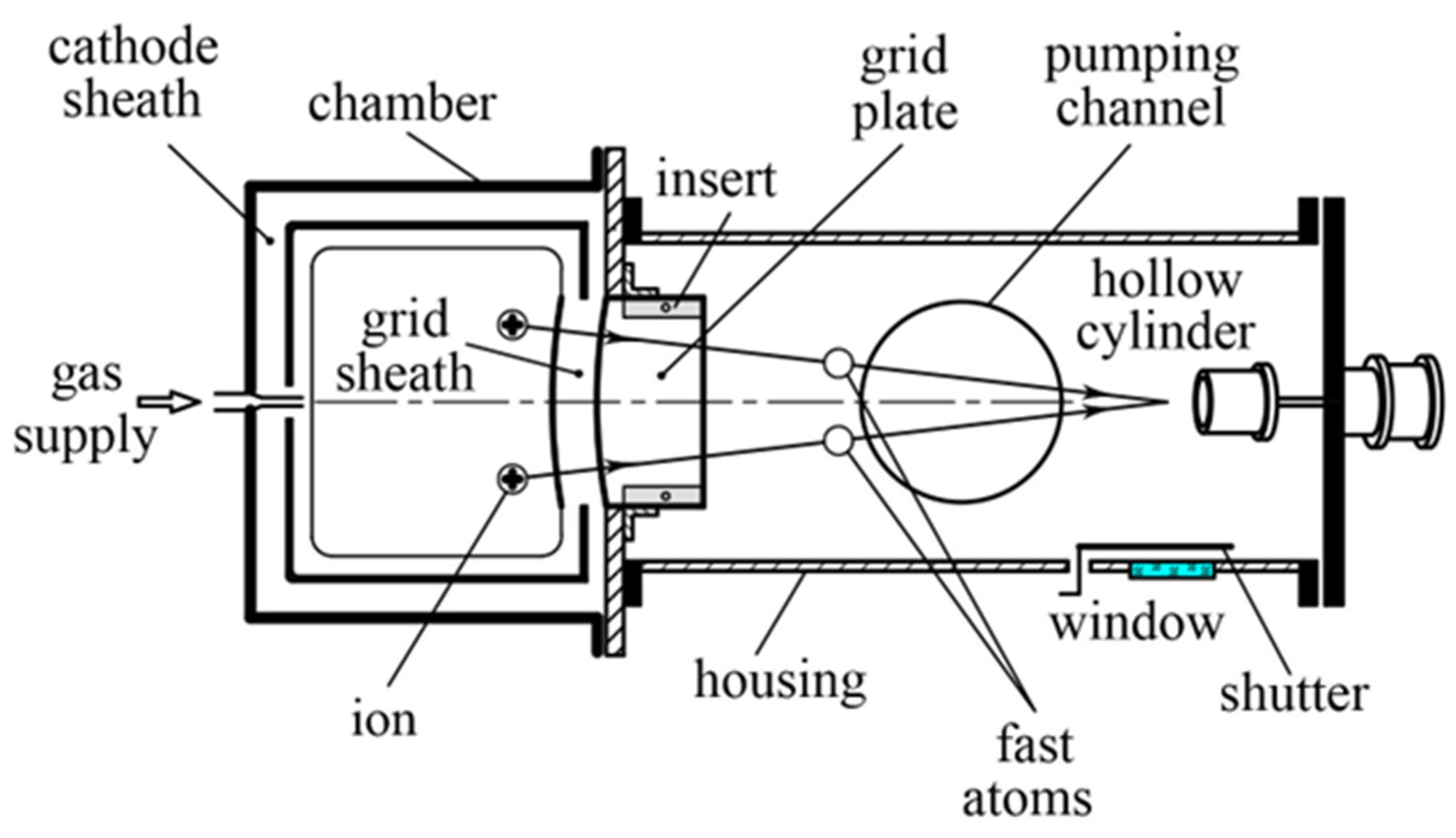
The experimental system for processing the internal surface of hollow ceramic samples is presented in Figure 1. It consists of a 36 cm diameter vacuum chamber and a rectangular housing, which is 70 cm long, 14 cm high, and 30 cm wide. There is inside the 35 cm long chamber a closed 34 cm long and 34 cm in diameter hollow cathode, which is fastened inside the chamber using 8 ceramic support isolators between them.
In the right wall of the chamber, there is a hole 7 cm high and 21 cm wide. The hole is covered with a grid consisting of plane-parallel titanium plates spaced 5 mm apart from each other. The thickness of the plates is 0.5 mm. The right wall of the hollow cathode is distant at 1 cm from the chamber wall and has a hole with the same width of 21 cm and height of 7 cm. Plates with 4.5 mm thick inserts between them are fastened together with tie rods. The accelerating grid is electrically connected to the chamber and the negative pole of the accelerating voltage power supply. Its positive pole is connected to the anode, which is inserted into the hollow cathode. Between the anode and the hollow cathode is connected a DC power supply.
Through a syringe-like stainless steel tube inserted through an orifice in the hollow cathode wall is continuously fed argon. It enters the housing through the grid and is evacuated from there by a turbomolecular pump.
Due to the curvilinear sheath between the plasma and the grid (Figure 2), trajectories of accelerated particles are directed to a focus distant at 60 cm from the grid.
On the removable flange is mounted a rotating holder for the sample. The angle between the axes of holder rotation and housing is 15°. On the housing top is mounted a magnetron sputtering system with a 10 cm in diameter cylindrical target made of TiB2.
After the chamber is pumped out, argon is fed into it and its pressure is set to 0.2 Pa. Then, a voltage of ~400 V between the anode and the cathode and a voltage of 2000 V between the anode and the grid are established, which results in glow discharge ignition. The discharge current Id is regulated in the range from 0.5 to 4 A by the discharge voltage Ud. For this purpose, an isolating transformer with insulation withstanding voltages up to 4 kV between the primary and secondary windings is used. The cathode and the grid currents are controlled with ammeters.
Due to the hollow cathode effect, the plasma inside the cathode is uniform [12], and the current density of ions emitted into the sheath between the plasma and the grid is close to the current density of ions on the surface of the cathode. The inner surface of the cathode Sc, including the area Sh = 147 cm2 of the 7 cm high and 21 cm wide hole in the cathode wall, is 5445 cm2. Hence, at the discharge current of 4 A, the mean ion current density is 0.7346 mA/cm2, and the ion currents in the circuits of the cathode and the grid should be Ic = 3.892 A and Ig = 0.108 A, respectively. Nevertheless, the ammeters showed that at the current in the cathode circuit of Ic = 4 A, the grid current is Ig = 0.2 A. It means that the plasma density near the grid approximately by two times exceeds the average value near the cathode surface.

2.2. Instruments for Characterization of the Samples

A stylus profiler Dektak XT manufactured by Bruker Nano, Inc. (Billerica, MA, USA) was used to measure the surface roughness, coating thickness, and thickness of the removed surface layer.
An infrared pyrometer IMPAC IP 140 manufactured by LumaSense Technologies GmbH (Frankfurt am Main, Germany) was used to measure the sample temperature.
Nanovea M1Hardness and Scratch Tester, produced by Nanovea Mechanical Testing (Irvine, CA, USA), was used to measure the coating microhardness and adhesion.
A Calotest instrument produced by CSM Instruments (Peseux, Switzerland) was used to evaluate the abrasion resistance of the samples.

3. Results

3.1. Sputtering

To study the processing of the internal surfaces of hollow ceramic samples using beams of fast argon atoms, 30 mm long hollow cylinders with an internal diameter of 30 mm and an external diameter of 40 mm made of aluminum oxide, silicon nitride, and zirconium dioxide were used. After fixing a sample in the holder and installing a removable flange with the holder and sample in place, the system was pumped down to ~0.001 Pa.
Turning on the rotation of the holder with the sample at a speed of 60 rpm, argon was fed to the system, and its pressure was set to 0.2 Pa. Switching on the power supplies ignited the glow discharge with the ion current in the cathode circuit of Ic = 4 A and the grid current of Ig = 0.2 A. At a distance of 5 mm between the grid plates and a plate thickness of 0.5 mm, the grid transparency is 0.9. Only 10% of the ions accelerated from plasma bombard edges of the plates, and the remaining 90% of the ions with an energy of 2 keV fly through the gaps between the grid plates. Because of contacts with plates, ions are transformed into fast neutral atoms. Because of the curvilinear grid sheath (Figure 2), the cross-section width of the beam propagating from the grid towards the sample is decreasing, and the cross-section height keeps a constant value of 7 cm. This is how a ribbon beam is formed in front of the sample.
To determine the beam cross-section, near the sample, a 0.5 mm thick titanium target was placed perpendicular to the beam axis. After the target irradiation by the beam for half an hour, the imprint on the target made it possible to measure the height of the beam cross-section of 7 cm and its width of about 2 cm. As the width of the beam cross-section near the accelerating sheath is 21 cm, the flow density of fast atoms increases by 10 times. Taking into account the grid current Ig = 0.2 A, grid transparency η = 0.9, and fast atom energy of 2 keV, we obtain the power carried by the beam equal to 360 W. For the beam cross-section of 7 × 2 = 14 cm2, the density of beam power heating the sample is 25.7 W/cm2 = 257,000 W/m2.
According to the Stefan–Boltzmann expression, treatment of a flat sample with a beam of such power density in a steady state can heat it to a temperature exceeding a thousand degrees. However, in our case, the thermal load is not so high because of the sample rotation at a speed of 60 rpm. Measurements of the sample temperature with a pyrometer through a quartz window on the lateral wall of the housing (Figure 2) showed that it does not exceed 700 °C.
To measure the sample’s sputtering rate, small masks were applied to the surface of the sample. The mask material was a water-based correction fluid with titanium dioxide (TiO2). The mask was applied to the sample with a brush and had the shape of a 2 mm diameter and 0.2 mm thick dot (after drying). After the sample had been treated with a fast atom beam for an hour, the masks were removed from its surface with a damp cloth soaked in an alcohol solution, and the height of the step between the masked and open surfaces was measured using a Dektak XT profilometer. Considering that fast argon atoms hit the surfaces of the mask and sample at an angle of 75°, the step can only be measured from the side where the atoms arrive, since on the opposite side of the mask, the sample surface is in the shadow of the mask, and the step is not formed.
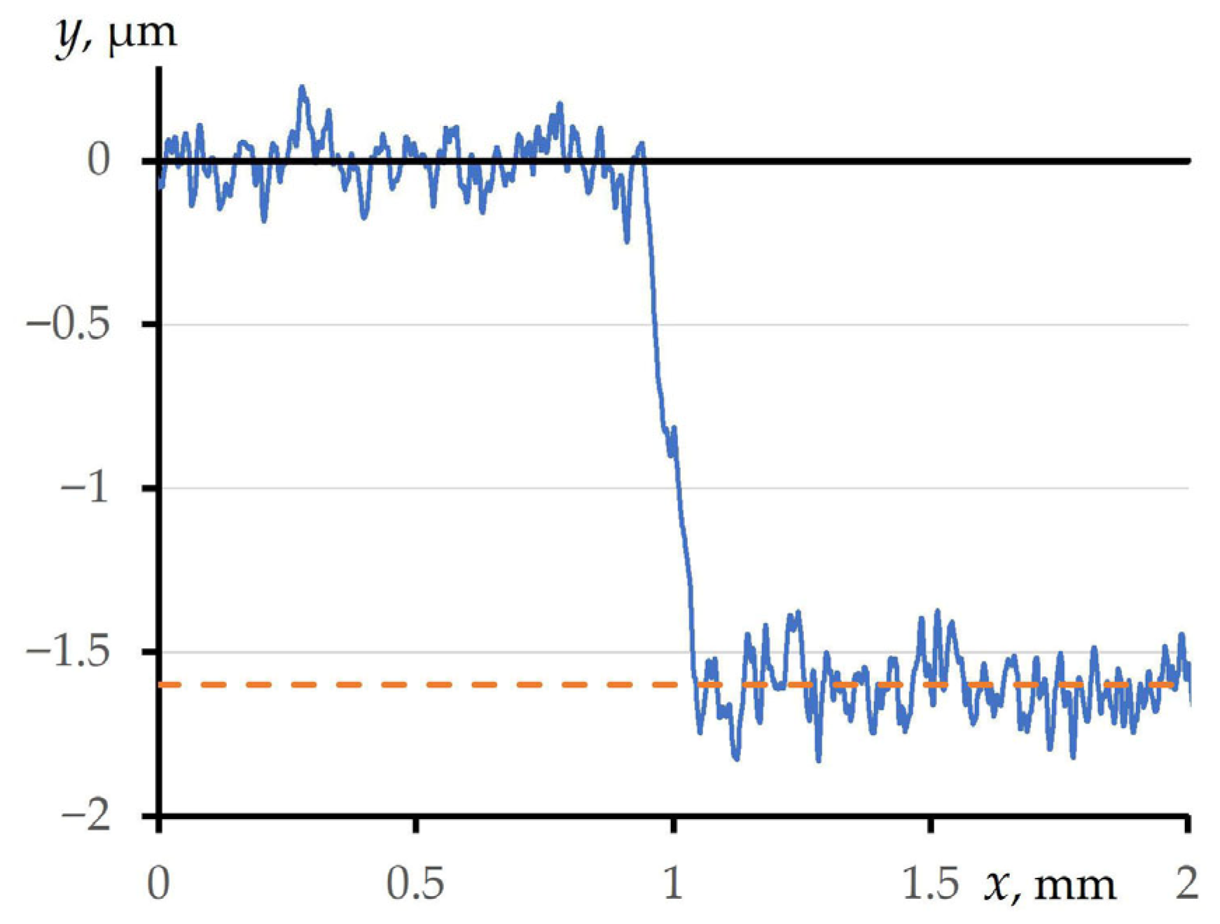
Figure 3 presents a profilogram of the external surface of an aluminum oxide sample with a masked area of 2 mm in diameter, located 3 mm from the edge of the sample. The height of the masked area over the surface surrounding it is equal to the thickness h = 1.6 µm of the removed surface layer.
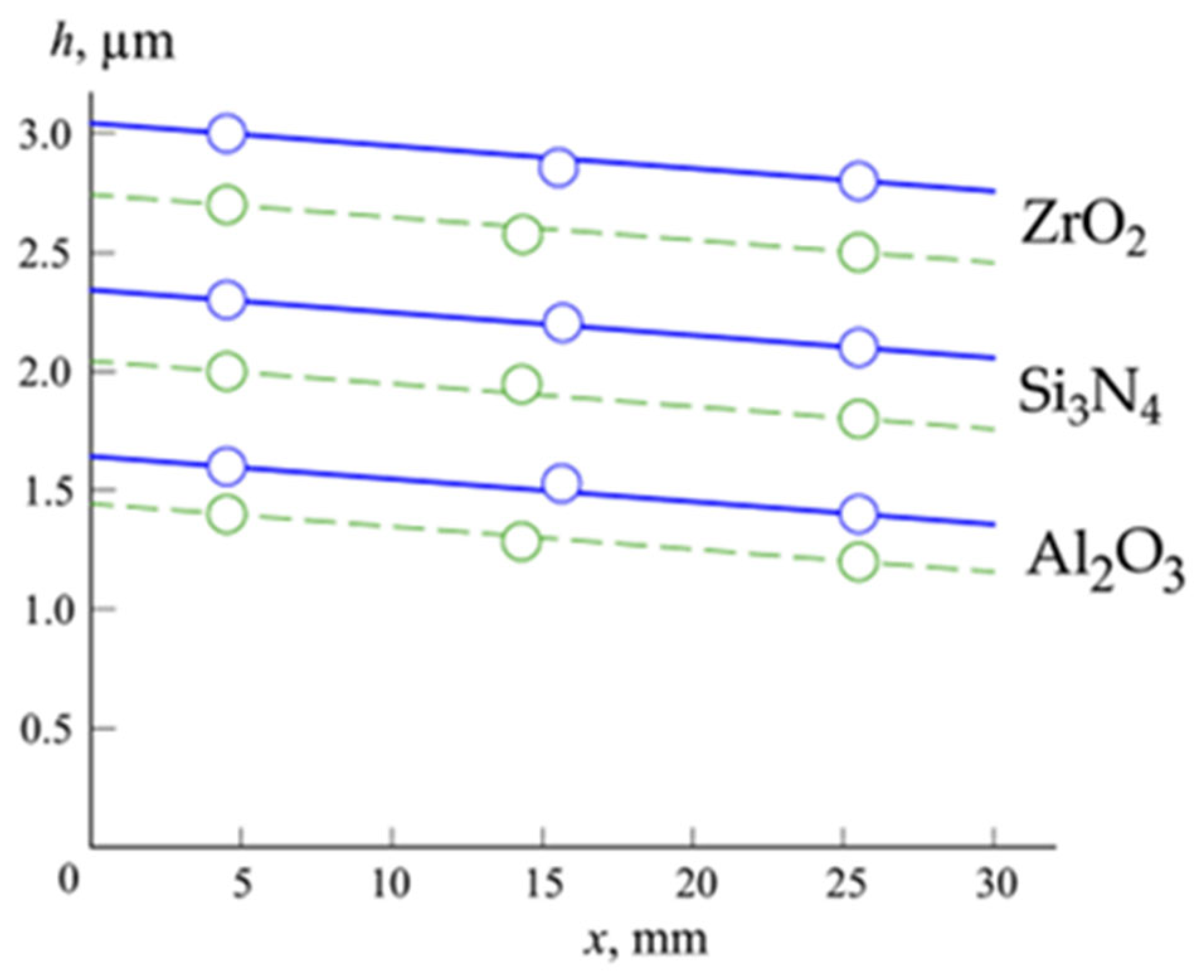
One more mask was applied in the middle of the external surface of the same sample, and two masks were applied to its internal surface. Figure 4 presents the dependence of the masked areas’ height h over the sputtered surface of the sample on the distance x from the sample edge. It shows that the sample surface is sputtered quite evenly. The thickness h of the removed layer on the outer side of the sample is 1.6 µm at a distance of 3 mm from the sample edge and decreases slightly to 1.4 µm at its opposite end. On the inner side of the sample, the thickness of the removed layer is h = 1.4 µm at a distance of x = 5 mm from the entrance of the beam into the sample cavity and slightly decreases to h = 1.2 µm at a distance of x = 25 mm.
The same measurements were carried out with two other samples of the same shape and size, but made of other ceramics—silicon nitride and zirconium oxide. Both samples were treated for one hour by argon atoms with the energy of 2 keV and a beam current of 0.18 A. Dependences of the removed surface layer thickness h on the distance x from the edges of the Si3N4 and ZrO2 samples are presented in Figure 4 together with the data for the Al2O3 sample.
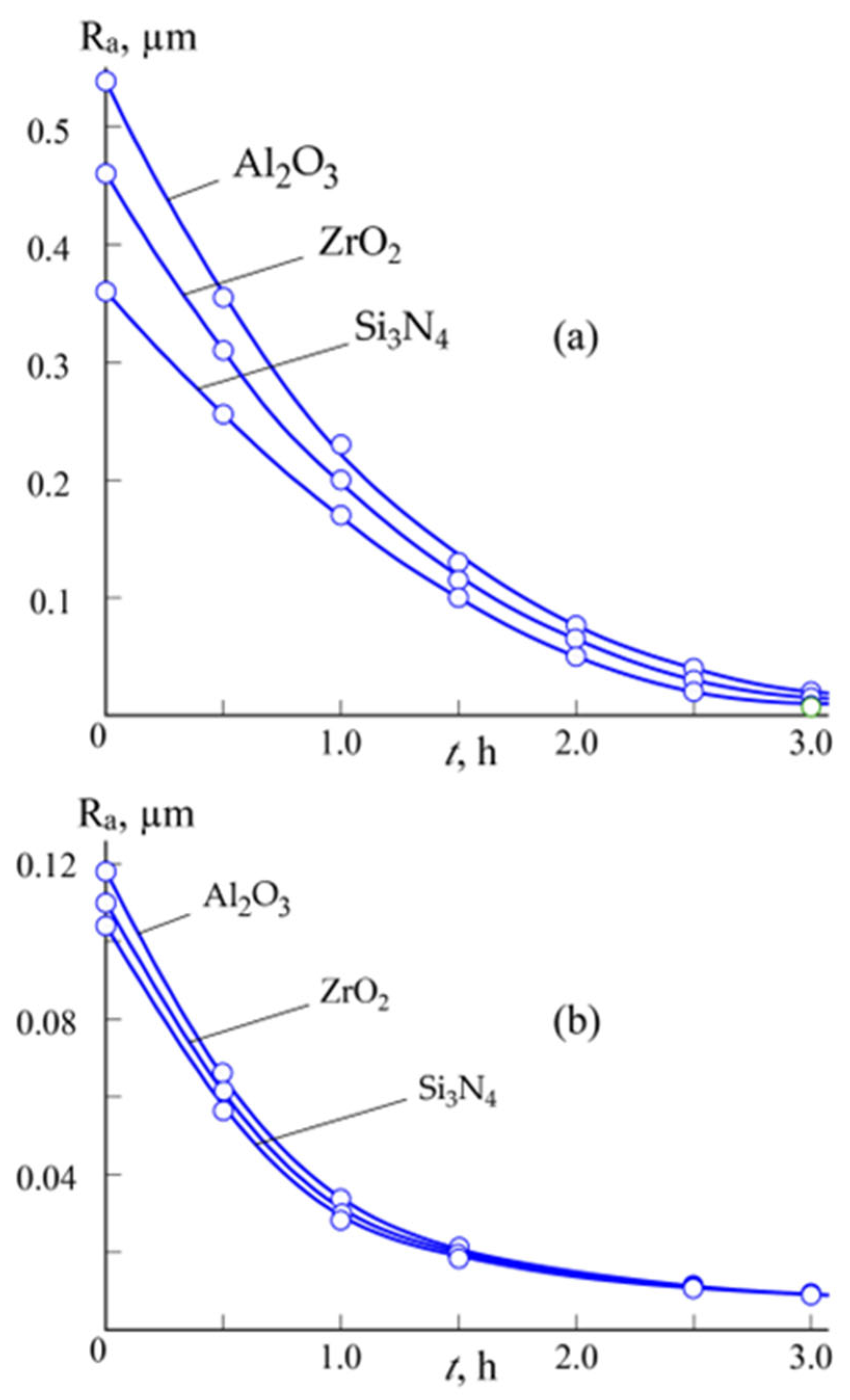
In all cases, the removed layer thickness is maximum at the entrance of the beam to the sample cavity and slightly decreases to its opposite end. For the silicon nitride sample, it decreases from 2.3 to 2.1 µm on its outer side and from 2.0 to 1.8 µm on its inner side. For the zirconium oxide sample, it decreases from 3.0 to 2.8 µm on its outer side and from 2.7 to 2.5 µm on its inner side. These results demonstrate a sufficient homogeneity of the beam-treated surfaces. The Dektak XT profilometer was also used for measuring the sample surface roughness Ra. Figure 5 presents the dependence of the sample surface roughness Ra on the treatment time t.
At first, for each hollow sample, the initial roughness was measured. It was Ra 0.118 µm for the outer sides of the Al2O3 sample and Ra 0.532 µm for its inner side, Ra 0.108 µm for the outer side of the ZrO2 sample and Ra 0.457 µm for its inner side, Ra 0.104 µm for the outer side of the Si3N4 sample and Ra 0.357 µm for its inner side.
It may be concluded that for all ceramic samples purchased to carry out experiments, the roughness of the inner surface is several times higher than that of the outer surface. It can be assumed that polishing the inner surface of the ceramic cylinder turned out to be a more difficult task for the manufacturer than polishing the outer surface.
After the Al2O3 sample was treated for half an hour by argon atoms with the energy of 2 keV and a beam current of 0.18 A, the roughness of its outer surface decreased from Ra = 0.118 µm to Ra = 0.062 µm, and the roughness of its inner surfaces decreased from Ra = 0.532 µm to Ra = 0.36 µm. When the same sample was returned to the housing and processed in the specified mode for another half hour, the roughness decreased to Ra = 0.040 µm and Ra = 0.224 µm for the outer and inner sides, respectively. A further treatment for more than an hour resulted in a decrease in the roughness to Ra = 0.008 µm for the outer and Ra = 0.08 µm for the inner side of the sample.
The obtained results show that sputtering of hollow ceramic cylinders with fast argon atoms at large angles of incidence on the surface is characterized by a fairly rapid decrease in surface roughness. The higher the roughness, the higher the rate of its reduction. After 3 h of processing, the roughness Ra of the internal surfaces decreases by an order of magnitude to ~Ra 0.02 μm and becomes closer to the roughness of the external surfaces ~Ra 0.01 μm.

3.2. Coating Deposition

Polishing ceramic products before deposition of wear-resistant coatings can improve their properties and extend their service life. In this study, we have chosen a TiB2 coating, which is remarkable for its high hardness, low resistivity, high melting point of 3225 °C, good adhesion resistance, and chemical stability.
A 10 cm diameter target made of TiB2 was mounted in the magnetron sputtering system at the top of the housing (Figure 1). The center of the target is distant from the removable flange of the housing by 10 cm. The power supply of the sputtering system ensures a magnetron target current up to 8 A. When the sputtering system is switched off, the target is protected from impurities with a movable shutter.
The trajectories of sputtered atoms from the magnetron target to the surface of a cylindrical sample differ significantly from the rectilinear trajectories of sputtered atoms arriving on a flat substrate [13,14,15]. However, low-energy sputtered atoms move by diffusion and therefore can deposit on all areas of the sample surface, both external and internal. For a flat substrate, the adhesion of the coating applied to the surface opposite the magnetron target is very poor. The adhesion can be improved when the growing coating is bombarded by energetic particles [16].
Small masks were used again to measure the thickness of the coatings applied to the surfaces of the cylindrical sample. The mask material was a water-based correction fluid with titanium dioxide (TiO2).
In the system shown in Figure 1, to ensure sufficient coating adhesion, the rotating sample was pre-treated for 10 min with a beam of fast argon atoms with an energy of 2 keV and a beam current of 0.18 A. Then the energy of fast atoms has been diminished to 1 keV, and the beam current decreased to 0.1 A. After switching on the magnetron power supply, deposition of the TiB2 coating started. The coating was bombarded during the deposition process with a beam of fast argon atoms with an energy of 1 keV and a current of 0.1 A.
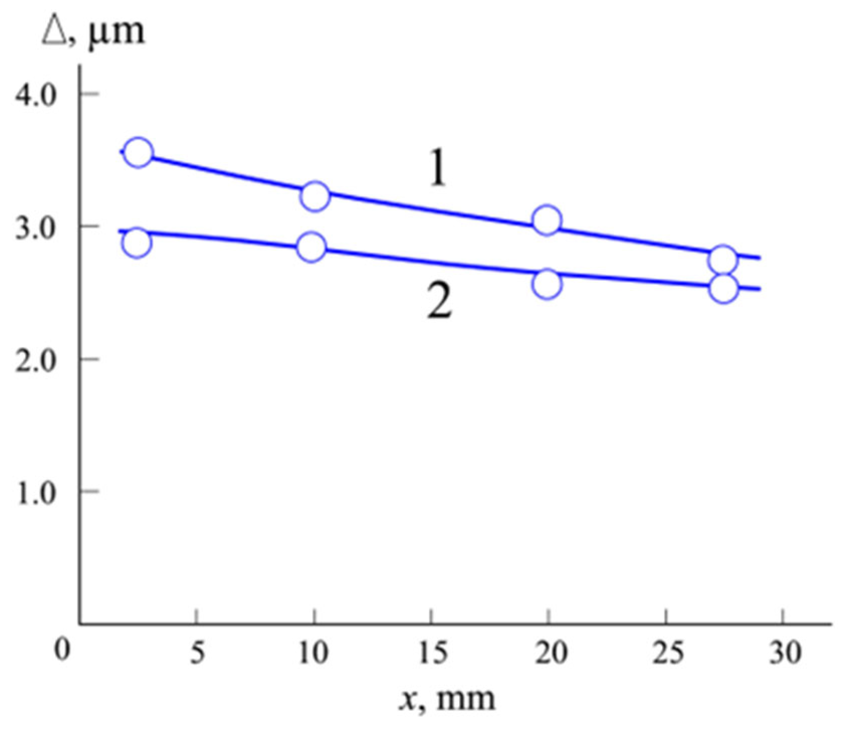
After a Si3N4 sample had been treated for an hour, the masks were removed from its surface with a damp cloth soaked in an alcohol solution, and the height of the step between the masked and open surfaces was measured using a Dektak XT stylus profilometer. Figure 6 presents dependencies of the coating thickness Δ on the distance x from the end of the sample on its outer (1) and inner (2) surfaces.
Similar measurements were carried out on two other samples of aluminum oxide and zirconium oxide. The results were identical to those obtained for the silicon nitride sample. This indicates that the thickness of the deposited coating is independent of the sample material. Since the data from these two samples overlap with the data from the zirconium oxide sample, in Figure 6, the latter characterizes all three materials.
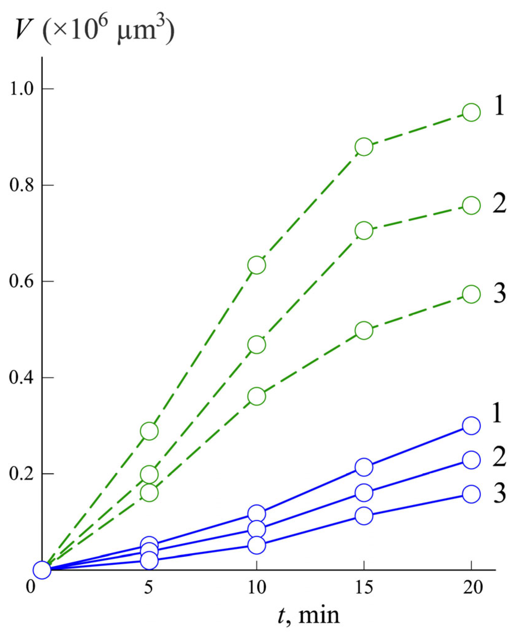
To determine how fast argon atom treatment and the application of a wear-resistant coating affect the wear resistance of hollow ceramic samples, their abrasive resistance was measured. For the convenience of measuring the abrasive resistance of the applied coating, fragments of 3 cm in length and 6 mm in width were cut from the samples along the generatrix of the cylinder. A Calotest instrument was used for measuring.
On a fragment cut from the sample, a rotating ball with a radius of R = 10 mm was placed with a load of 0.2 N, and into the contact zone, an abrasive suspension was supplied. As a result of the rotation of the ball, the abrasive particles form an elliptical depression on the surface of the sample. The major axis d of the depression is measured using an optical microscope. The abrasive wear can be characterized by the volume V of material worn from the sample depression. Since the major axis d of the depression is many times smaller than the radius of the ball, the volume of worn material can be determined by the formula V = (π∙d4/64R)[r/(r ± R)]0.5, in which the “+” sign is for a depression on the outer (convex)surface of the samples with a radius r = 20 mm and “−” for a depression on the inner (concave) surface with a radius r = 15 mm [17].
Figure 7 presents the dependencies of the abrasion volume V on the test time t for zirconium oxide, silicon nitride, and aluminum oxide samples before treatment and after deposition of 3.5 µm thick TiB2 coatings on polished surfaces of the samples.
The obtained results show that, as a result of the samples’ treatment with a beam of fast argon atoms and the application of a wear-resistant TiB2 coating, abrasive wear was reduced by approximately three times.
For characterization of the coating applied to the sample, a Hardness and Scratch Tester with a diamond Rockwell Indenter tip (R = 100 μm) was used. The coating microhardness amounted to 2150 HV40. The first critical load to result in the appearance of an acoustic emission and first cracks on the coating amounted to 18 N. It should be mentioned that the first critical load of TiN coatings applied to flat WC substrates never exceeded 14 N. Quite a good adhesion was achieved due to the surface activation by the fast argon atoms before the coating deposition and the coating bombardment by the fast argon atoms during the deposition process.

4. Discussion

The coatings applied to ceramic products can substantially improve their quality. As the coating’s properties depend on the surface conditions, they are desired to be improved before the coating. Usually, this is realized through cleaning and polishing the product surface with energetic particles, accelerated ions [18,19,20,21] or fast atoms [8,9,22,23]. Previously, beams of fast neutral atoms were produced due to charge exchange collisions of accelerated ions with gas molecules [24,25].
In the case of products with cavities, other technical solutions are required [26,27]. We proposed to use a ribbon beam of fast argon atoms at a high angle of incidence [28,29] for sputtering of the inner and outer surfaces of a rotating cylinder. When the angle between the axes of rotating sample and housing amounts to 15°, the upper half of the beam cross-section sputters at an angle of incidence of 75° the upper part of the inner surface of the rotating sample, and the lower half of the beam cross-section sputters at an angle of incidence of 75° the lower part of its outer surface (Figure 1). By rotating the sample at 60 rpm, the coating is continuously deposited on its surface and is periodically treated with fast atoms for half a second after a half-second pause. At a coating deposition rate of 10 μm/h, the thickness of coating deposited per one revolution is ~3 nm, which is easily penetrated by fast atoms with an energy of 2 keV. This ensures an increased strength and density of the coating.
The tests showed that polishing the inner and outer surfaces of a complex-shaped sample with fast argon atoms allows for the reduction in the surface roughness from Ra ~ 0.5 µm to Ra ~ 0.02 µm within 3 h (Figure 5). Treatment of the ceramic surface by fast argon atoms at an angle of incidence exceeding 75° allows for a significant increase in the surface finish class.

5. Conclusions

  • Using beams of fast argon atoms, it is possible to deposit wear-resistant coatings on inner surfaces of complex-shaped products and noticeably increase their wear-resistance.
  • Polishing a product with a beam of fast argon atoms with a large angle of incidence on its surface makes it possible to reduce the surface roughness to Ra ~ 0.01.
  • Due to pretreatment of the products with a beam of fast neutral atoms, before the deposition of wear-resistant coating, the coating adhesion was substantially improved, and the abrasive wear became three times smaller.

Author Contributions

Conceptualization, A.S.M., M.A.V. and S.N.G.; methodology, A.S.M. and M.A.V.; software, E.S.M.; validation, A.S.M., M.A.V. and Y.A.M.; formal analysis, Y.A.M.; investigation, E.S.M. and Y.A.M.; resources, E.S.M. and Y.A.M.; data curation, M.A.V. and Y.A.M.; writing—original draft preparation, A.S.M. and M.A.V.; writing—review and editing, A.S.M. and S.N.G.; visualization, E.S.M.; supervision, A.S.M. and S.N.G.; project administration, M.A.V.; funding acquisition, A.S.M. All authors have read and agreed to the published version of the manuscript.

Funding

This research was funded by the Russian Science Foundation, grant no. 23-19-00517.

Institutional Review Board Statement

Not applicable.

Informed Consent Statement

Not applicable.

Data Availability Statement

The data presented in this study are available on request from the corresponding author.

Acknowledgments

The study was carried out with the equipment of the center of collective use of MSUT “STANKIN”.

Conflicts of Interest

The authors declare no conflicts of interest.

References

  1. Danilov, I.; Hackert-Oschätzchen, M.; Zinecker, M.; Meichsner, G.; Edelmann, J.; Schubert, A. Process Understanding of Plasma Electrolytic Polishing through Multiphysics Simulation and Inline Metrology. Micromachines 2019, 10, 214. [Google Scholar] [CrossRef]
  2. Chirkov, A.M.; Rybalko, A.P.; Rogalsky, Y.I.; Sedoy, E.A.; Merkuhin, A.V.; Borisov, N.V. The Method of Laser-Plasma Polishing of a Metallic Surface. RF. Patent RU 2381094, 10 February 2010. [Google Scholar]
  3. Obeidi, M.A.; McCarthy, E.; O’Connell, B.; Ahad, I.U.; Brabazon, D. Laser Polishing of Additive Manufactured 316L Stainless Steel Synthesized by Selective Laser Melting. Materials 2019, 12, 991. [Google Scholar] [CrossRef]
  4. Koval, N.N.; Teresov, A.D.; Ivanov, Y.F.; Petrikova, E.A. Pulse Electron-Beam Metal Product Surface Polishing Method. RF. Patent RU 2619543, 16 May 2017. [Google Scholar]
  5. Abdul-Kader, A. Surface modifications of PADC polymeric material by ion beam bombardment for high technology applications. Radiat. Meas. 2014, 69, 1–6. [Google Scholar] [CrossRef]
  6. Škereň, T.; Veselý, M.; Čapek, P.; Král, J. Ion-induced nanopattern propagation on metallic surfaces. Phys. Rev. B 2015, 92, 235406. [Google Scholar] [CrossRef]
  7. Ieshkin, A.E.; Kushkina, K.D.; Kireev, D.S.; Ermakov, Y.A.; Chernysh, V.S. Polishing superhard material surfaces with gas-cluster ion beams. Tech. Phys. Lett. 2017, 43, 95–97. [Google Scholar] [CrossRef]
  8. Maishev, Y.P.; Shevchuk, S.L.; Kudrya, V.P. Generation of fast neutral beams based on closed drift ion sources. Russ. Microelectron. 2014, 43, 345–351. [Google Scholar] [CrossRef]
  9. Nam, S.K.; Economou, D.J.; Donnelly, V.M. Generation of fast neutral beams by ion neutralization in high-aspect-ratio holes: A particle-in-cell simulation study. IEEE Trans. Plasma Sci. 2007, 35, 1370–1378. [Google Scholar] [CrossRef]
  10. Ruset, C.; Grigore, E. The influence of ion implantation on the properties of titanium nitride layer deposited by magnetron sputtering. Surf. Coat. Technol. 2002, 156, 159–161. [Google Scholar] [CrossRef]
  11. Grigore, E.; Ruset, C.; Short, K.; Hoeft, D.; Dong, H.; Li, X.; Bell, T. In situ investigation of the internal stress within the nc-Ti2N/nc-TiN nanocomposite coatings produced by a combined magnetron sputtering and ion implantation method. Surf. Coat. Technol. 2005, 200, 744–747. [Google Scholar] [CrossRef]
  12. Metel, A.S.; Grigoriev, S.N.; Melnik, Y.; Panin, V.V. Filling the vacuum chamber of a technological system with homogeneous plasma using a stationary glow discharge. Plasma Phys. Rep. 2009, 35, 1058–1067. [Google Scholar] [CrossRef]
  13. Anders, A. Tutorial: Reactive high power impulse magnetron sputtering. J. Appl. Phys. 2017, 121, 171101. [Google Scholar] [CrossRef]
  14. Kelly, P.J.; Arnell, R.D. Magnetron sputtering: A review of recent developments and applications. Vacuum 2000, 56, 159–172. [Google Scholar] [CrossRef]
  15. McDaniel, E.W. Collision Phenomena in Ionized Gases; Willey: New York, NY, USA, 1964. [Google Scholar]
  16. Kaminsky, M. Atomic and Ionic Impact Phenomena on Metal Surfaces; Springer: Berlin/Heidelberg, Germany, 1965. [Google Scholar]
  17. Rutherford, K.L.; Hutchings, I.M. Micro-scale abrasive wear testing of PVD coatings on curved substrates. Tribol. Lett. 1996, 2, 1–11. [Google Scholar] [CrossRef]
  18. Kaufman, H.R. Broad-beam ion sources. Rev. Sci. Instrum. 1990, 61, 230–235. [Google Scholar] [CrossRef]
  19. Kaufman, H.R.; Hughes, W.E.; Robinson, R.S.; Tompson, G.R. Thirty-eight-centimeter ion source. Nucl. Instrum. Methods Phys. Res. B 1989, 37–38, 98–102. [Google Scholar] [CrossRef]
  20. Hayes, A.V.; Kanarov, V.; Vidinsky, B. Fifty-centimeter ion beam source. Rev. Sci. Instrum. 1996, 67, 1638–1641. [Google Scholar] [CrossRef]
  21. Vizir, A.V.; Yushkov, G.Y.; Oks, E.M. Further development of a gaseous ion source based on low-pressure hollow cathode glow. Rev. Sci. Instrum. 2000, 71, 728–730. [Google Scholar] [CrossRef]
  22. Grigoriev, S.; Melnik, Y.; Metel, A. Broad fast neutral molecule beam sources for industrial-scale beam-assisted deposition. Surf. Coat. Technol. 2002, 156, 44–49. [Google Scholar] [CrossRef]
  23. Metel, A.S.; Grigoriev, S.N.; Melnik, Y.A.; Bolbukov, V.P. Broad beam sources of fast molecules with segmented cold cathodes and emissive grids. Instrum. Exp. Technol. 2012, 55, 122–130. [Google Scholar] [CrossRef]
  24. Phelps, A.V. Cross sections and swarm coefficients for nitrogen ions and neutrals in N2 and argon ions and neutrals in Ar for energies from 0.1 eV to 10 keV. J. Phys. Chem. Ref. Data 1991, 20, 557–573. [Google Scholar] [CrossRef]
  25. Phelps, A.V.; Greene, C.H.; Burke, J.P. Collision cross sections for argon atoms with argon atoms for energies from 0.01 eV to 10 keV. J. Phys. B At. Mol. Opt. Phys. 2000, 33, 2965–2981. [Google Scholar] [CrossRef]
  26. Moll, E.; Bergmann, E. Hard coatings by plasma-assisted PVD technologies: Industrial practice. Surf. Coat. Technol. 1989, 37, 483–509. [Google Scholar] [CrossRef]
  27. Cui, X.; Wang, D.; Guo, J. Effects of material microstructure and surface microscopic geometry on the performance of ceramic cutting tools in intermittent turning. Ceram. Int. 2018, 44, 8201–8209. [Google Scholar] [CrossRef]
  28. Metel, A.S.; Volosova, M.A.; Melnik, Y.A.; Mustafaev, E.S.; Grigoriev, S.N. Removal of Wear-Resistant Coatings from Cutting Tools by Fast Argon Atoms. Coatings 2023, 13, 999. [Google Scholar] [CrossRef]
  29. Grigoriev, S.N.; Metel, A.S.; Volosova, M.A.; Mustafaev, E.S.; Melnik, Y.A. Polishing Ceramic Samples with Fast Argon Atoms at Different Angles of Their Incidence on the Sample Surface. Plasma 2024, 7, 816–825. [Google Scholar] [CrossRef]
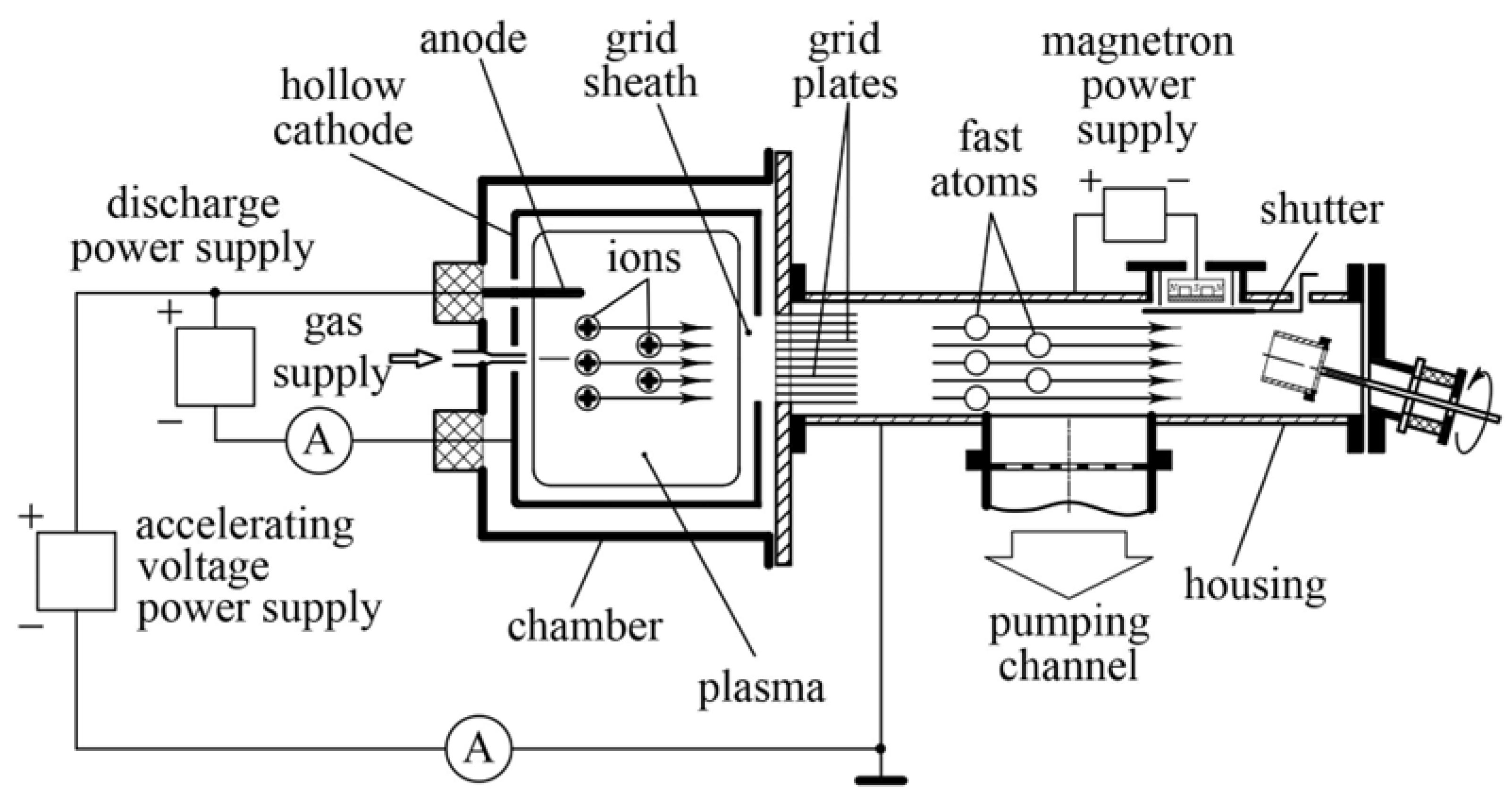
Figure 1. Schematic of a system for the treatment of hollow ceramic samples.
Plasma 08 00047 g001
Figure 2. A system for the treatment of hollow ceramic samples (top view).
Plasma 08 00047 g002
Figure 3. Profilogram of the external surface of the sample, the left part of which refers to the surface covered with a mask and the right part to the open surface sputtered by fast argon atoms. The difference between the two levels gives the thickness h = 1.6 µm of the surface layer removed.
Plasma 08 00047 g003
Figure 4. The thickness h of the removed surface layer versus the distance x from the edge of the hollow sample made of Al2O3, Si3N4, or ZrO2 on its outer (full lines) and inner (dashed lines) sides.
Plasma 08 00047 g004
Figure 5. Dependences of the sample roughness Ra on its inner (a) and outer (b) surfaces on the time t of treatment with a beam of fast argon atoms.
Plasma 08 00047 g005
Figure 6. Distribution of coating thickness Δ on the outer (1) and inner (2) surfaces of the samples made of ZrO2, Si3N4, and Al2O3 ceramics at a distance x from the sample end.
Plasma 08 00047 g006
Figure 7. Dependence of the abrasion volume V on the test time t for ZrO2 (1), Si3N4 (2), and Al2O3 (3) samples before processing (dashed lines) and after polishing the sample surface and application of wear-resistant coating (full lines).
Plasma 08 00047 g007
Disclaimer/Publisher’s Note: The statements, opinions and data contained in all publications are solely those of the individual author(s) and contributor(s) and not of MDPI and/or the editor(s). MDPI and/or the editor(s) disclaim responsibility for any injury to people or property resulting from any ideas, methods, instructions or products referred to in the content.