Review

Pixel Circuit Designs for Active Matrix Displays

1
School of Electrical Engineering & Intelligentization, Dongguan University of Technology, Dongguan 523808, China
2
School of Information and Optoelectronic Science and Engineering, South China Normal University, Guangzhou 510631, China
3
State Key Laboratory of Luminescent Materials and Devices, South China University of Technology, Guangzhou 510640, China
4
Centre for Atomaterials and Nanomanufacturing, School of Science, RMIT University, Melbourne, VIC 3000, Australia
*
Authors to whom correspondence should be addressed.
Appl. Syst. Innov. 2025, 8(2), 46; https://doi.org/10.3390/asi8020046
Submission received: 3 February 2025 / Revised: 21 March 2025 / Accepted: 28 March 2025 / Published: 31 March 2025
(This article belongs to the Section Control and Systems Engineering)

Abstract

:
Pixel circuits are key components of flat panel displays, including liquid crystal displays (LCDs), organic light-emitting diode displays (OLEDs), and micro light-emitting diode displays (micro-LEDs). Depending on the active layer material of the thin film transistor (TFT), pixel circuits are categorised into amorphous silicon (a-Si) technology, low-temperature polycrystalline silicon (LTPS) technology, metal oxide (MO) technology, and low-temperature polycrystalline silicon and oxide (LTPO) technology. In this review, we outline the fundamental display principles and four major TFT technologies, covering conventional single-gated TFTs to novel two-gated TFTs. We focus on novel pixel circuits for three glass-based display technologies with additional mention of pixel circuits for silicon-based OLED and silicon-based micro-LED.

1. Introduction

1.1. Display Technology

Since the 1950s, display technologies have evolved and active matrix liquid crystal displays (AM-LCDs), active matrix organic light-emitting diode displays (AM-OLEDs), and active matrix light-emitting diode displays (AM-LEDs) have become the dominant technologies for direct-viewing applications such as smartphones, televisions, and monitors [1,2]. These displays typically have large panel sizes (ranging from 5 inches to 85 inches), glass substrates, and wide viewing angles (160° to 180°), as shown in Table 1. AM-LCDs are the most mature technology, which use a backlight unit that transmits light through the LCD panel and converts white light into red, green, and blue light through colour filters [3]. They are known for their low power consumption, high contrast, and low cost [3,4]. AM-OLEDs utilise organic materials to emit light independently and offer high colour accuracy, flexibility, and higher brightness (2000–7000 cd/m2) compared to AM-LCDs [5,6,7,8]. However, their lifetimes are significantly shorter under high brightness or high voltage conditions [9]. AM-LEDs, especially Micro-LEDs, are a promising technology due to their high brightness, high efficiency, and long lifetime. It employs micron-sized inorganic LEDs as light-emitting pixels with excellent brightness (500–1200 cd/m²) and long lifetime [10,11]. Despite their great potential, AM-LEDs face technical challenges such as complex fabrication processes and driver-integrated circuit design, which hinder their widespread application [12].
Near-eye projection displays are a key technology for Augmented Reality (AR) and Virtual Reality (VR) applications, with high-resolution density LCDs, liquid crystal on silicon (LCoS), silicon-based OLEDs, and silicon-based LEDs being the main technologies [13]. These micro-displays are characterised by, among other things, small panel sizes (0.3–2.5 inches) and extremely high pixel densities (800–7000 PPI), which are critical for delivering sharp images when viewed at close ranges [14,15]. High-resolution density LCDs have proven manufacturing processes and low cost for mass production, but their performance is limited by flicker effects, small aperture ratios, and colour mixing effects [16]. LCoS is known for its high-resolution density and fast response time, but its performance is constrained by the fringe field effect and finite voltage swing [17]. Silicon-based OLEDs have the characteristics of autonomous light emission, thinness, and flexibility, but their manufacturing process is complex, leading to yield and cost issues, and their lifetime issues limit their applications [18]. Silicon-based LED technologies have attracted attention for their ability to achieve high performance metrics, including fast optical response, low power consumption, and high contrast [19]. However, they also face unique challenges, such as giant transfer technology, full-colour technology [20], and driver technology. Due to the characteristics and size of micro-display devices, complex driving circuits are required to control the brightness and colour of each pixel, which places extreme demands on circuit design and fabrication. For example, variations in current can cause the central wavelength of micro-LEDs to shift, resulting in colour deviations [21]. Ultra-high resolution OLEDs and micro-LED displays have extremely small pixel pitches (ranging from tens of microns to less than ten microns) [22,23]. The reduced pixel pitch increases the electrode resistance and contact resistance, leading to preferential current flow through the low-resistance path. This leads to an increase in local current density and triggers current crowding effects, which reduces efficiency and increases leakage current [24]. These issues make designing suitable pixel circuits more challenging but can be mitigated by advanced thin-film transistor (TFT) technology and sound pixel circuit design (e.g., dynamic compensation techniques)

1.2. Driver Types

Displays are classified into static and dynamic drivers based on the addressing method. The dynamic driver included a passive matrix and an active matrix (AM) (Figure 1) [25]. The PM (passive matrix) illuminates pixels by progressive scanning, with each pixel emitting light for a shorter period of time, resulting in limited brightness and difficulty in displaying complex information, whereas AM, by equipping each pixel with an independent switching device (e.g., a TFT), enables continuous illumination and supports higher brightness and more complex image displays, thus accommodating more information. For instance, the emission of each pixel in an AM-OLED is often controlled through switching devices like TFTs. Each pixel at the intersection of the scan lines and data lines has an associated switching device. The signals from the data lines regulate the intensity of each pixel’s emission, with scan lines addressed sequentially [26,27,28]. AM technology has been widely used in smartphones, TVs, etc.
A crucial component in the advancement of the display field is switching devices. It includes TFTs and MOSFETs. TFTs are used for glass-based displays, and MOSFETs are used for silicon-based displays. The switching device determines the running and stopping of each pixel and affects the key parameters of each pixel’s luminescence, such as frame rate, power consumption, and resolution display. Since MOSFETs are well known, this review focuses on TFTs.

1.3. TFT Devices

At present, TFTs are mainly classified according to semiconductor materials into amorphous silicon (a-Si) TFTs, low-temperature polycrystalline silicon (LTPS) TFTs, and metal oxide (MO) TFTs [26]. Their TFT characteristics are shown in Table 2.

1.3.1. a-Si TFT

a-Si TFTs have been the mainstream TFT for TFT-LCD since the commercialisation of TFT-LCD in the early 1970s [29]. a-Si is an amorphous material with a low process temperature, simple production, mature technology, and low cost. The mobility affects the driving current and switching speed of the TFT. The mobility of the a-Si TFT is only 0.1–1 cm2/Vs. If a-Si TFT is used for high-current driven AM-OLED and AM micro-LED displays, its drive current is typically increased by enlarging the width-to-length ratio of the TFT. However, expanding the TFT’s width increases parasitic capacitance and restricts the pixel aperture ratio, leading to a low PPI [29,30]. Moreover, a-Si TFT exhibits the worst VTH stability, which compromises display stability. Due to this unresolved issue, applying a-Si TFTs to AM-OLED or AM micro-LED commercial products is challenging [30]. Therefore, a-Si TFTs are primarily used in low-resolution LCDs [31].

1.3.2. LTPS TFT

LTPS TFT represents the next-generation TFT technology after a-Si TFT. LTPS TFT is made using a laser crystallisation process and possesses excellent electrical characteristics, with field-effect mobility of up to 50–200 cm2/(Vs), higher than that of a-Si TFT and MO TFT [32]. The LTPS TFT has fast switching speeds. It can be fabricated with small size and low parasitic capacitance, which results in high-resolution displays [33,34]. However, LTPS material is difficult to prepare at low temperatures and large areas [3]. Their fabrication techniques and equipment differ from conventional a-Si TFTs, resulting in higher process costs than a-Si and MO TFTs. As a result, LTPS TFTs are mainly used in small and medium-sized high-resolution displays.

1.3.3. Metal Oxide TFT
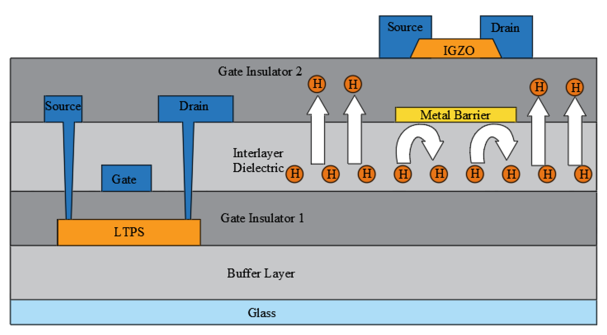
Metal oxide (MO) TFT [35] represents a compromise between a-Si TFT and LTPS TFT. Its representative device is IGZO TFT. The mobility of the MO TFTs lies in the middle of the a-Si TFT and the LTPS TFT. Both a-Si and MO TFTs have amorphous microstructures, in contrast to the polycrystalline microstructure of LTPS TFTs. Thus, a-Si and MO TFTs share similar fabrication, scaling, and cost characteristics [29,30]. Moreover, MO TFTs have a low leakage current (about 1 pA) compared to LTPS. Leakage current is a critical indicator of TFT performance [36,37]. When the leakage current is high, even if the pixel circuit is not operating, the charge stored in the storage capacitor is constantly consumed, resulting in a decrease in panel brightness. Pixel circuits with a diode-connected structure may increase the brightness due to additional current injection when the leakage current is high. However, this undoubtedly increases the complexity of the circuit design. Therefore, a high leakage current leads to increased power consumption, making it challenging to achieve low frame rate displays and fine grey-level adjustments [38]. The leakage current of MO TFT is several orders of magnitude smaller than that of a-Si TFT and LTPS TFT [39]. Thus, MO TFTs currently offer a suitable low-cost solution for large-size high-resolution displays [40]. In addition, MO TFT has the characteristics of flexibility and transparency. The combination of MO TFTs with flexible substrate can achieve flexible and transparent displays [41,42,43]. This technology has broad application prospects in wearable devices.

1.3.4. LTPO TFT

LTPO TFT consists of LTPS TFT and MO TFT, first proposed by Apple Inc. [44]. In the pixel circuit, MO TFTs with low leakage current are connected to the signal lines, and LTPS TFTs with high driving capability are used for power supply. This enables low frame rate (1 Hz) operation with low power consumption [45,46]. LTPO TFTs are usually available in two combinations. The first is a combination of top-gate LTPS TFTs and bottom-gate MO TFTs (Figure 2), while the second combination includes top-gate LTPS TFTs and top-gate oxide TFTs [47].
Hydrogenation is often used to enhance the characteristics of LTPS TFTs. However, MO TFTs are easily affected by hydrogen, resulting in reduced reliability [45]. Therefore, balancing the total amount and distribution of hydrogen atoms in LTPO stacks during manufacturing is crucial. Current solutions include low hydrogen insulating silica layer techniques. [46], metal barrier processes [48] that prevent hydrogen diffusion from the bottom layer, combined BG LTPS TFT and TG MO TFT configurations [47], and others.

1.3.5. Double-Gate TFT

The performance of TFTs described in previous sections is based on single-gate (SG) TFTs. Double-gate TFTs (DG TFTs) consist of two opposing gates (Figure 3). In 1981, Luo et al. first developed DG TFTs using CdSe as an active layer for flat panel display applications [49]. In DG TFTs, two parallel channels emerge when voltages are applied to the top and bottom gate electrodes. DG TFTs can flexibly adjust the position of the channel and the carrier transport path, which significantly mitigates the effect of material defects [50]. This improves carrier mobility and reduces the subthreshold slope (SS) [50,51]. SS is the slope of the relationship between gate voltage and drain current. A small SS indicates high switching speed and precise controllability of the TFT device [52]. Moreover, due to the effective active layer width, DG TFTs have a greater drive current than SG TFTs. Therefore, DG TFTs can be applied to displays with high frame rates. Another advantage of DG TFTs is their on-state voltage controllability, where the VTH can be adjusted as a function of the applied top gate bias voltage, determined by the capacitance ratio of the two gate dielectrics [53]. This characteristic serves to support the adaptability of circuit design.

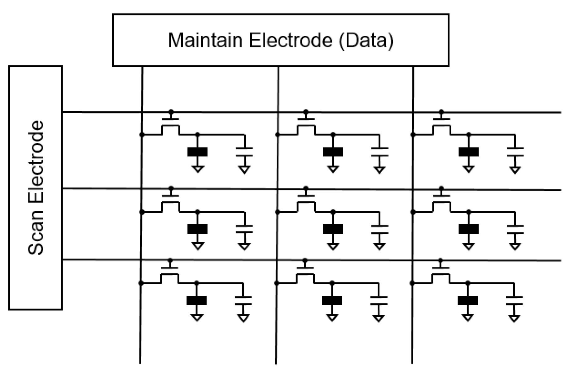
2. TFT-LCD Pixel Circuits

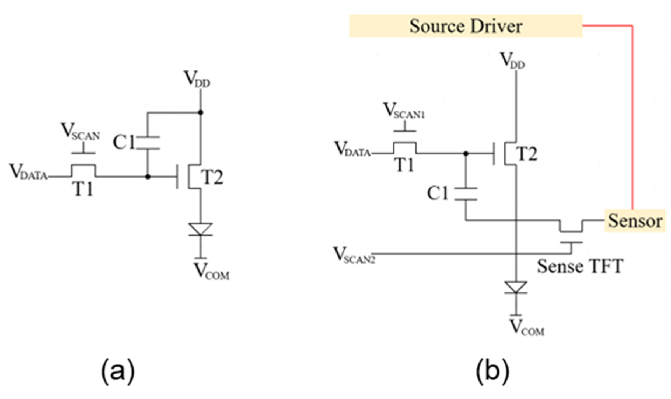
2.1. TFT-LCD Typical Pixel Circuits

A TFT-LCD typical circuit consists of one TFT and one capacitor (Figure 4); it was used in early TFT-LCD displays. When the TFT is turned on, the data signal is added to both ends of the LCD pixel through the drain and stored in the capacitor at the same time. The liquid crystal is distorted at a specific angle to form a greyscale display [1]. LCDs are voltage-driven devices. TFT-LCD has low requirements for TFT driving capability. Thus, mature processes and low-cost a-Si TFT are the main choices for low PPI TFT-LCD [55,56]. However, the mobility of a-Si TFT is too low, and it is difficult to implement more versatile displays. In addition, displays using a-Si TFT consume more power. To meet the development of the display industry, including low power consumption, high frame rate, high contrast ratio, etc., the choice of TFTs shifted to high-mobility TFTs.

2.2. TFT-LCD Novel Pixel Circuits

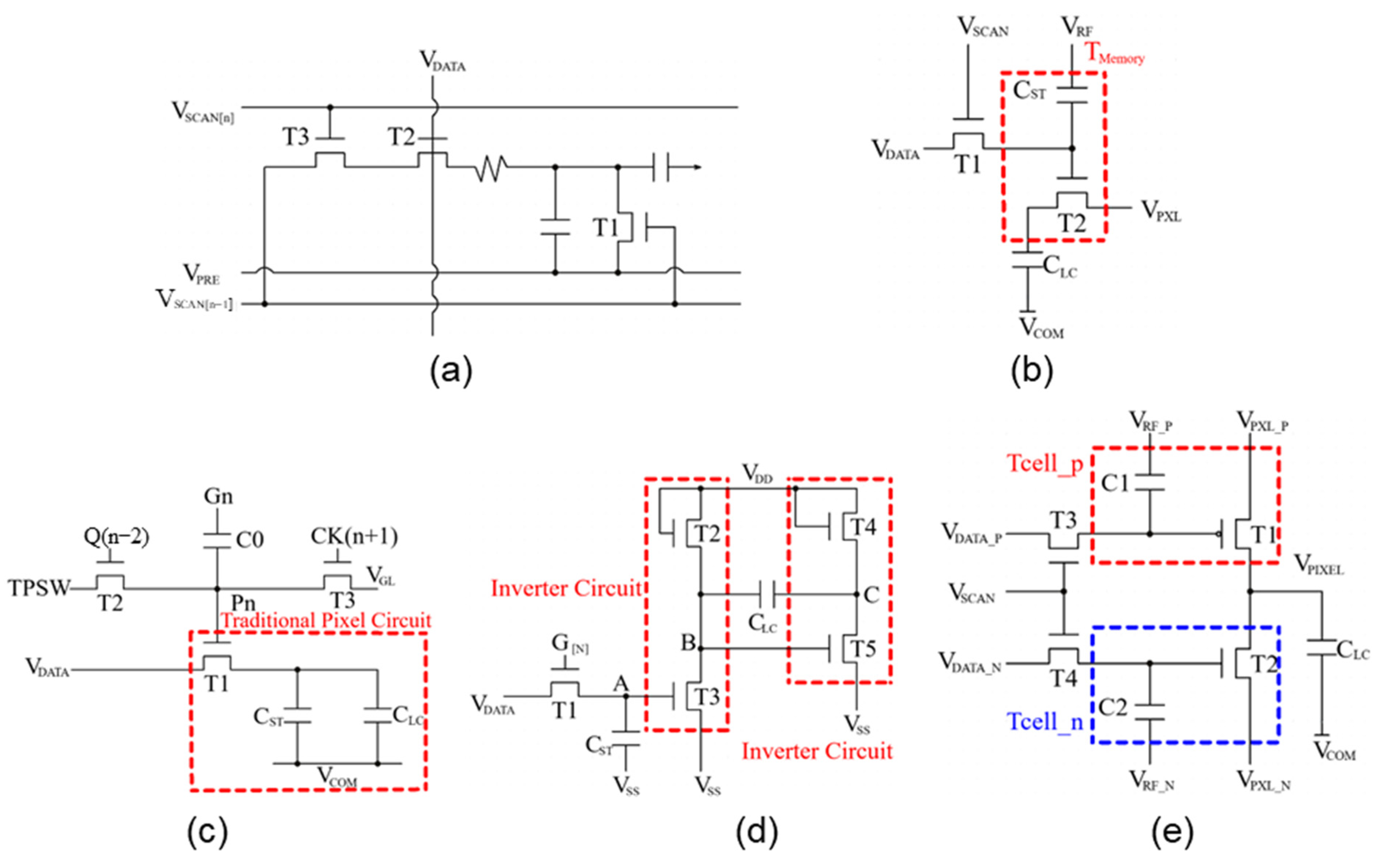
  • LTPS TFT LCD pixel circuits
The mobility of LTPS TFTs is two orders of magnitude higher than that of a-Si TFTs. LTPS TFT is usually applied to small and medium-sized LCDs with great performance. Of all the electronic modules in an LCD, the data driver is second only to the backlight in power consumption [57], with most of the power used to convert signals from digital-to-analogue. To reduce the power consumption in this part, some researchers envisioned that the pixel circuit would take on more of the driving function.
Yahsiang Tai’s team proposed a novel digital drive pixel circuit [57], which can integrate the function of a digital-to-analogue converter into a pixel. Consequently, a traditional data driver’s signal conversion component can be removed, significantly lowering power usage. According to Figure 5a, the proposed pixel circuit utilises LTPS TFTs with small SS as a dynamically switched driver pixel circuit, which contains two series-connected TFTs (T2 and T3) and a resistor to form a discharge route for the pixel voltage. The pulse width of the data source controls T1 for presetting the pixel voltage and when the scanning voltage enables the pixel. The VPRE is a direct current source that can be used as a common voltage for both the storage capacitor and the preset voltage. Compared with the conventional 1T1C pixel circuit, the pixel circuit is suitable for high-definition displays despite the smaller aperture.
Cao, H. et al. of China Star Optoelectronics Technology (CSOT) utilised the dynamic frame rate driving method to design a pixel circuit (Figure 5c) with a boost function [58], which can achieve a 5–120 Hz wide frame rate display. The circuit can increase the current flowing through the driver TFTs by boosting the Vgs of the TFTs in the active area to improve the charging performance without increasing the supply voltage. Compared to conventional IT1C circuits, this circuit increases the number of external signal lines and TFTs, resulting in a decrease in the panel’s aperture ratio. To improve the applicability of this technique, the precharged TFT (T2) and the pull-down TFT (T1) in this row share settings on both sides of each row. Sharing the TFTs makes it possible to easily connect the signals of TPSW (TP switch is the switching signal needed to achieve the in-unit touch panel) and GAS1 (GAS1 is the control signal needed to achieve all gates), which avoids routing the wires in pixel areas. The charge ratio of the 120 Hz optimal circuit panel was improved by 6% compared to the normal design. Meanwhile, BOE’s self-developed 4KReal240Hz technology effectively reduces motion trailing and improves dynamic clarity through two-frame over driving technology and optimises the charging process of the LCD unit with multi-level clock technology to significantly improve charging efficiency, further solving the display challenges at high refresh rates [62].
The above innovative circuit designs or driving techniques, such as dynamic frame rate driving, overdrive technology, and multi-stage clocking technology, are commonly used in displays with high refresh rates, low power consumption, and smooth displays to address the issues of power consumption and charging efficiency. However, increased circuit complexity brings challenges such as reduced opening rates or complex wiring.
2.
MO TFT LCD pixel circuits
Blue phase liquid crystal display (BPLCD) applications have two key problems, namely high operating voltage and frequency effects. For BPLCD to achieve better applications, Lin et al. suggested an IGZO TFT pixel circuit with an inverter topology [59]. The circuit (Figure 5d) consists of five TFTs and two capacitors, where T2 and T3, and T4 and T5 form two sets of inverter circuits. By leveraging these two sets of inverter circuits, the circuit can reach a higher operating voltage, which in turn allows the BPLCD to attain enhanced transmittance. The high-frequency effect is suppressed by generating a current that continuously charges the BPLCD, thus preventing the BPLCD from storing insufficient charge during the hold period and reducing the greyscale voltage. This circuit eliminates the need for a conventional common signal (COM) and improves the pixel opening ratio. It is worth noting that inverter topologies are commonly used in LCDs to provide high voltage power to the backlight and are not common in pixel circuits.
3.
LTPO TFT LCD pixel circuits
The low leakage current of LTPO TFT reduces the power consumption of the display, and the pixel voltage can be maintained for a long time without refreshing. Therefore, LTPO TFT can be used in automotive displays that require long display times. To further reduce power consumption, some researchers have combined LTPO technology with low refresh rate memory-in-pixel (MIP) circuits for liquid crystal displays [63,64] and achieved the desired results.
Based on a previous study, Jo, J. et al. at Kyung Hee University proposed a self-refreshing multiphase MIP circuit with a simple structure for low-power LCDs [60]. The circuit consists of driver transistors (T1 and T2), programming transistors (T3 and T4 are oxide-TFTs with low leakage current), and storage capacitors (C1 and C2). The operating process consists of three phases: the programming phase, the refresh phase, and the emission phase. During the programming phase, the scanning signal turns on the programming transistors T3 and T4 in turn, through which VDATA_P and VDATA_N are programmed at the gate nodes of the driver transistors T1 and T2, respectively. After the programming phase, the row and column drivers are turned off and therefore do not consume power. During the negative polarity refresh phase, VPXL_N and VRF_N act on all pixels simultaneously. All pixels sequentially follow VPXL_N until a pixel-specific voltage corresponding to the programmed data voltage in each pixel is reached. When a still image is displayed, all pixels are refreshed at the same time instead of the traditional 1T1C line-by-line refresh, which consumes much more power. Compared to SRAM-type MIP [63], this circuit uses a simple multilevel memory cell to achieve multilevel greyscale adjustment with higher aperture ratios and pixel densities.
Currently, LTPO is less used in TFT-LCD products. As the technology develops, we may see more LCD technology combined with LTPO, especially in terms of energy savings and refresh rate optimisation.
4.
Double-gate TFT LCD pixel circuits
Oxide-TFTs have the advantage of low leakage current, their carrier mobility can be increased, and subthreshold swing can be reduced using a double gate structure to achieve better device performance. Jo, J. et al. proposed a self-refreshing multilevel memory-in-pixel circuit for reflective low-power LCD including oxide-TFTs [61]; the circuit consists only of two DG IGZO-TFTs and one storage capacitor (Figure 5b). The two gates of this TFT are connected for driving, and VRF and VPXL are global signal lines connected to the gate and source of the TMemory (composed of T2 and CST), respectively. Its working process consists of three phases: the programming phase (TPRG), the refresh phase (TRF), and the display phase (TDISP). Programming phase: the data voltage is programmed in the pixels. Refresh phase: all pixels are simultaneously refreshed according to the data voltages programmed in the programming phase, the refresh process of which is not depicted in detail here. In the display phase, the pixel voltages are retained. At the end of TDISP, they are reversed to the opposite polarity to prevent image residue. The circuit repeats the self-refresh operation without additional programming until the desired image is updated. Because there is no need to program the data voltage, both the scan driver and the data driver can be idle. Instead, dynamic power consumption is used in the global signal lines (VRF and VPXL) for self-refresh because all pixels are refreshed simultaneously instead of line-by-line, and the drive frequency is significantly reduced.
Compared to the latest multilevel MIP circuits for LTPO TFTs [60], the MIP circuits containing only MO TFTs are simpler, have lower costs, and have better uniformity in fabrication. The simple structure of this MIP circuit allows for higher resolution. In addition, due to the small leakage current of MO TFT, the frame rate can be reduced from 60 Hz to 1 Hz, and the power consumption is lower than that of traditional circuits. Thus, this circuit has the advantage of simultaneously achieving high performance and low power consumption.

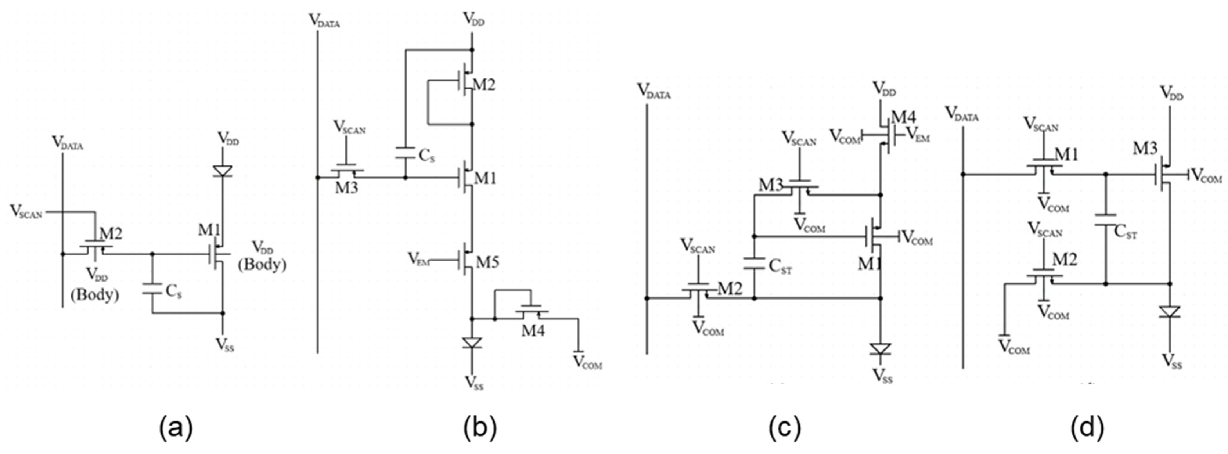
3. OLED Pixel Circuits

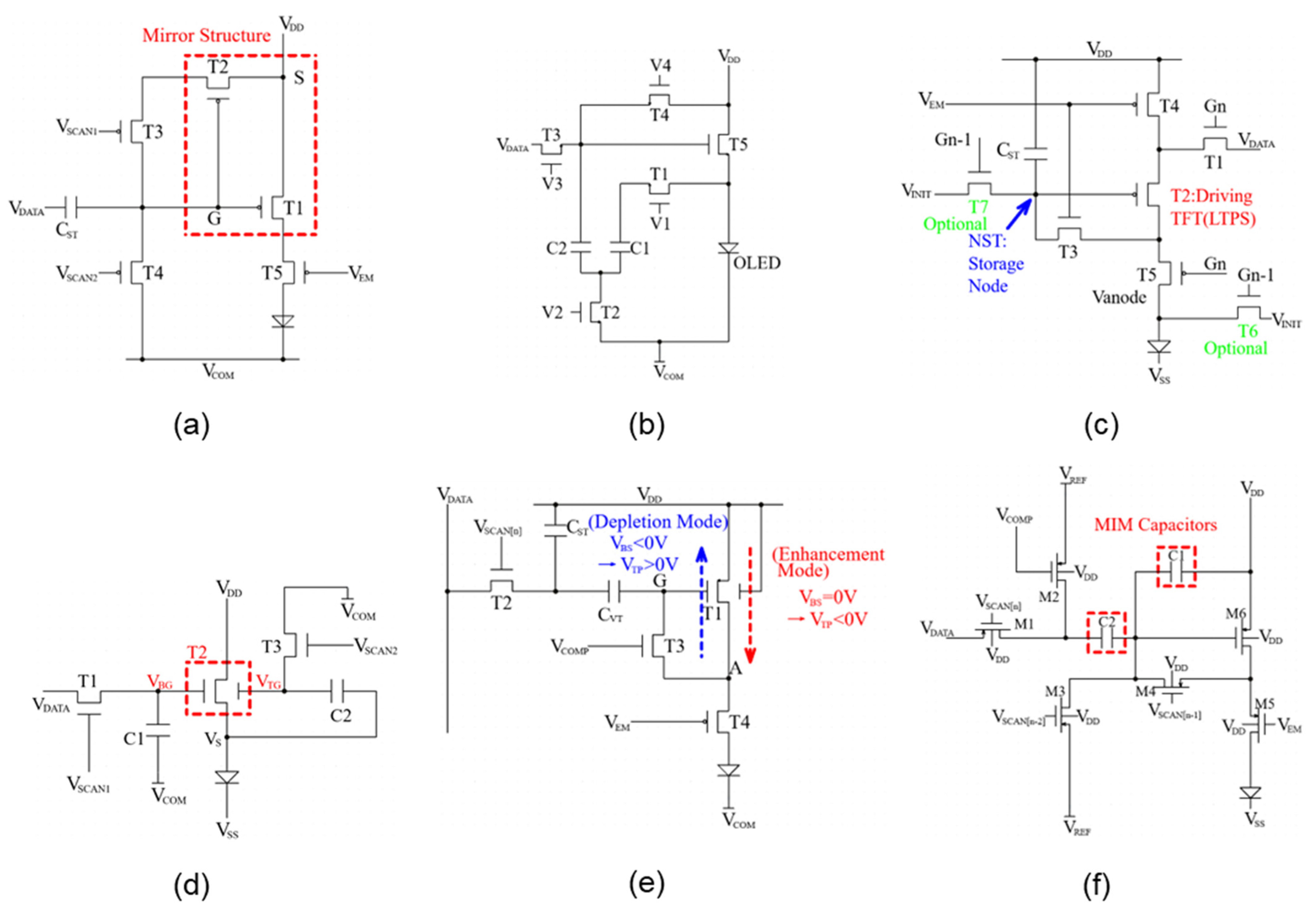
3.1. OLED Typical Pixel Circuits

OLEDs are current-driven devices with display brightness proportional to the current flowing through them. This driving characteristic places stringent requirements on the driving capability and stability of the TFT. Designing and fabricating pixel circuits for OLEDs is more challenging than for TFT-LCDs [56]. 2T1C is the basic pixel circuit [40] shown in Figure 6a. When VSCAN is at high voltage, the data signal VDATA enters the internal pixel circuit through T1 and is stored in the capacitor Cl. When the Cl storage voltage exceeds the threshold voltage of T2, T2 provides the current for the continuous OLED lighting. During this process, the switching TFT requires a low leakage current to prevent the capacitor discharge. The driving TFT remains on throughout the frame cycle, continuously passing current to the OLED, requiring a high current transfer capability [56].
LTPS TFTs and MO TFTs are currently the mainstream TFT technologies for OLED displays because of their good electrical characteristics. OLEDs operate by converting VDATA to pixel current. However, both LTPS TFTs and IGZO TFTs exhibit unequal field effect mobility and VTH when manufactured over a broad area due to manufacturing issues [65,66]. Their gates are biased at a fixed voltage for long periods, causing VTH shift [66,67]. These shifts result in the uneven display. To address the aforementioned VTH shift issue and increase the uniformity of OLED current, AM-OLED panels must employ compensatory mechanisms. There are two types of compensating methods: external compensation and internal compensation [34,68].
Figure 6. Typical 2T1C pixel circuit (a) and external compensation (b) [69].
Asi 08 00046 g006
External compensation circuits (Figure 6b) facilitate simple pixel circuit structures. This method not only reduces the effects of TFT defects and simplifies drive signals but also improves aperture ratios and enables narrow-bezel designs. LGD successfully developed an 88-inch 8K OLED by using an external compensation method to detect and compensate for mobility and VTH in real time [70]. Its pixel circuit is a simple 3T1C circuit and has no compensation function. Its external circuit requires an analogue-to-digital converter, a sensing data memory, a compensation algorithm unit, etc., making it more complex than the internal compensation method. The external compensation method requires an external IC, increasing the cost compared to the internal compensation method.
Internal compensation circuits can be categorised as voltage programming circuits and current programming circuits according to the type of compensation. In the voltage programming method, the VDATA is written to the gate of the drive TFT through a selector switch and stored in a storage capacitor [27]. Voltage programming circuits have been extensively studied and mass-produced due to their high compensability and ease of manufacture. Typical examples include the 4T2C circuit reported by Dawson [71], the 6T1C circuit of Samsung [72], etc. For current programming pixel circuits, mainstream compensation structures include the non-mirrored current source method [73] and the mirrored current source method [74]. Current current-programmed pixel circuits can effectively cope with the VTH shift problem of driving TFTs, but this is not the main reason for adopting current programming. However, such circuits have limitations in high-frequency display applications due to the large RC delay of the data lines at low currents, which results in long signal build-up times [75].

3.2. OLED Novel Pixel Circuits

3.2.1. LTPS TFT OLED Pixel Circuits

LTPS TFT OLED pixel circuits are well developed, and their pixel compensation circuits can address IR drop variations in addition to VTH shifts in some cases [76]. As display resolution improves, pixel circuits must achieve the same or better compensation effect with fewer devices. Li Y. et al. of Nanhua University presented a 5T1C pixel circuit based on LTPS TFT [77], as shown in Figure 7a. The circuit can extract VTH and mobility by forming a mirror structure of T1 and T2. The circuit generates an adaptive voltage at the TFT gate during the programming phase, compensating for the VTH shift and mobility change. The circuit uses one less capacitor than the 5T2C pixel circuit of Yeonkyung Kim’s team [68], achieving a better area effect. Moreover, T5 is controlled by VEM to turn on only in the emission phase, so this circuit prevents image flickering. To address the high leakage current problem of LTPS TFTs, some researchers have proposed using the high potential to suppress and successfully reduce storage drive voltage fluctuation [78].

3.2.2. MO TFT OLED Pixel Circuits

The VTH instability of MO TFTs increases the OLED current error in a pixel circuit. Aryamick Singh proposed an IGZO TFT 5T2C pixel circuit (Figure 7b) that utilises the common diode-connected transistor method to compensate for spatial and temporal VTH variations in the driving TFT [79]. During the VTH detection phase, capacitor C1 is charged to VrefVTH, ensuring that the OLED current is unaffected by changes in the driver transistor threshold voltage during the emission phase. The circuit provides a constant current to the OLED, with an error is 1.05% (IOLED = 2.5 μA). Compared to other pixel circuits [80,81], this circuit displays the smallest IOLED error.
To improve the AM-OLED panel’s frame rate, Xie, Y. et al. from Shanghai Jiaotong University proposed 6T2C voltage-programmed pixel circuits with a simplified working cycle [82]. Its working cycle includes only the initial phase, the data input phase, and the emission phase. Its working cycle is a shorter VTH generation cycle compared with the classical voltage-programmed pixel circuit. This design may achieve a high frame rate.

3.2.3. LTPO TFT OLED Pixel Circuits

LTPO technology is widely used in high-performance devices such as Apple’s iPhone series and Samsung’s Galaxy S series due to its low frame rates and low power consumption [83]. Its functions can be understood through Royole’s pixel and GOA circuit designs [84]. The pixel circuit design (shown in Figure 7c) contains several functional modules: the control branch consists of MO TFTs, which are responsible for resetting the anode node (Vanode) and programming the data and compensation information to the storage node (NST), and the drive branch consists of high-mobility, high-current LTPS TFTs (T2, T4, and T5), which conduct the current from the VDD during the emission process to the This design combines the high stability, low hysteresis, and good VTH compensation characteristics of LTPS TFTs, while eliminating the degradation effect of OLEDs by connecting the LTPS TFTs directly to the OLED anode, since the OLED current is controlled only by VDD and VDATA. In addition, MO TFTs as switches can be designed for small sizes due to their low drive capacity requirements, but the process incompatibility between MO TFTs and LTPS TFTs leads to complex manufacturing processes, production difficulties, and high costs of LTPO, which poses a challenge for their large-scale applications.

3.2.4. Double-Gate TFT OLED Pixel Circuits

The display frame rate of the display can be increased by decreasing the RC time constant. Conventional methods include increasing the TFT active layer width and reducing the capacitance driving the TFT [85]. The disadvantage of increasing the TFT active layer width is that it reduces the aperture ratios. Reducing the parasitic capacitance of TFTs can be achieved by introducing device structures with self-aligning properties, such as coplanar structures. However, coplanar MO TFTs usually require higher drive voltages, leading to higher power consumption and shorter device lifetime [86]. DG TFTs exhibit better electrical characteristics, such as steeper SS, than conventional SG TFTs [87]. Studies show that the switching speed of DG IGZO TFT circuits with the TG offset structure is more than tripled [88]. Thus, the DG structure can improve the display frame rate.
LGD developed the DG structure (Figure 3), which has higher mobility (29 cm2/Vs) and a smaller SS (0.2 V/dec) for the BG of the DG TFT than that of the TG. LGD proposed a simple 3T2C pixel circuit (Figure 7d) by utilising the properties of this structure [54]. The driver TFT (T2) is a DG IGZO TFT. The circuit uses the source tracking method to extract the VTH. The source tracking method works on the principle that the voltage at the source (i.e., the output voltage) follows the gate voltage using the relationship between the source and gate of the TFT. Specifically, the TFT’s source voltage will be approximately equal to its gate voltage minus the threshold voltage (VTH). This allows the source voltage to follow the input signal over a range of variations. Pixel circuits in OLED displays typically use source tracking to stabilise pixel currents and voltages, ensuring that the display is clear and consistently bright. The circuit employs a more mobile BG in the compensation process, which shortens the VTH sampling time (4 to 5 μs) and enables fast VTH compensation.
Based on Apple’s LTPO pixel circuit, Lee, J. et al. at Seoul National University developed a novel LTPO 4T2C pixel circuit (Figure 7e) utilising a synchronous emission scheme by combining DG LTPS TFTs and LTPO [89]. In this circuit, T2 and T3 are low-leakage-current IGZO TFTs constituting switching TFTs, and T1 and T4 are DG LTPS TFT and SG LTPS TFT devices, respectively, constituting the driving branch. The circuit cleverly regulates the potential high and low between the source and drain of the DG LTPS TFT, thus switching the current flow direction and putting T1 into two different operating states, i.e., positive depletion mode or enhancement mode. In the initial phase, the G-node is discharged to VSS using the positive depletion mode. In the compensation phase, the G-node is charged using the enhancement mode, and the G-node potential is changed to “VDD + VTP”. When the data voltage is transmitted to the pixel, the voltage difference “VDATAVREF” is transmitted to the G-node through CVT capacitive coupling, and the G-node voltage becomes “VDD + VTP + VDATAVREF”. Therefore, the VGS of T1 becomes “VDATAVREF + VTP”, and the current of T1 is determined by “VDATAVREF”, which is not affected by the characteristics of T1. In the emission phase, since the OLED is connected to the drain of T1, even if T1 is driven in saturation mode, the degradation of the OLED current and voltage characteristics does not have any effect on the emission current, which improves the uniformity of the display.
Figure 7. 5T1C mirror structure pixel circuit (a) [77], 5T2C pixel circuit (b) [79], 7T1C pixel circuit (c) [84], 3T2C pixel circuit (d) [54], LTPO 4T2C pixel circuit (e) [89], MOSFETs and three-MIM-capacitor pixel circuit (f) [90].
Asi 08 00046 g007
Compared to Apple’s 6T1C circuit, this circuit reduces two control lines and two TFTs used to initialise the gate-source bias (VGS) for driving the TFTs by modulating the bottom gate bias (VBS) of the DG LTPS-TFTs, resulting in improved pixel density, which is obtained at 538 ppi per inch using the 2 μm design rule.
TFT-LCD and AM-OLED pixel circuit design issues and methods
Issue CategorySolutionsExamples of TFT-LCDExamples of AM-OLED
Pixel chargingImprove TFT mobility,
optimise driving waveforms
3T1C [58]/
Refresh rate and response timeHigh-speed TFT design,
overdrive technology
3T1C [58,59], 4T2C [61]6T2C [82], 7T1C [84], 3T2C [54], 4T2C [89]
Power consumption Use low-power materials,
dynamic power management
3T2C [57], 5T2C [60]7T1C [84], 3T2C [54], 4T2C [89]
High resolution and high PPIHigh-mobility TFT,
new pixel structures
4T2C [61]3T2C [54], 4T2C [89]
VTH shift Internal compensation circuits (integrated compensation transistors and capacitors),
use high-stability TFT materials
/5T1C [77], 5T2C [79], 7T1C [84], 3T2C [54]
Mobility variationMobility compensation circuits,
improve manufacturing processes to enhance TFT uniformity
/5T1C [77]

3.2.5. Silicon-Based OLED Pixel Circuits

For silicon-based micro-OLED displays, the pixels occupy only micro-square meters due to densities exceeding 3000 pixels per inch. The current range of micro-OLED is very small, ranging from only a few hundred pico-amps to a few tens of nano-amps. A small current can alleviate the lifetime problem of OLED at high brightness and high current density [91], but whether its lifetime hours are sufficient for some applications still needs to be determined on a case-by-case basis. Notably, the VGS of the transistors in the pixel circuit needs to be regulated within a narrow range in the subthreshold region. Current grows exponentially, and VTH needs to be compensated for even with complementary metal oxide semiconductors (MOSFETs) exhibiting small VTH variations [90].
The SF method usually involves using the source of a MOSFET as the output and the gate as the input. This method is used to ensure that the voltage signal follows the input signal and to reduce voltage distortion. The CD method controls the voltage by dividing the voltage signal across two capacitors, using the voltage division principle of the capacitors. To solve the problem of narrow VDATA range problem, source follower (SF) and capacitive division (CD) methods have been proposed for silicon-based pixel compensation circuits (Figure 8). The SF utilises OLED or diode-connected transistors as source loads to extend the VDATA range from the gate node to the source node [92,93]. CD utilises a metal–insulator–metal (MIM) integrated capacitor and parasitic gate capacitance of the drive transistor, which are two capacitors, to extend the VDATA range [94,95].
Compared to TFTs, variations in the source bulk voltage (VSB) of MOSFETs cause variations in VTH, resulting in a bulk effect problem. However, the SF and CD methods do not solve this problem, and their driver transistors have different source voltage levels in the compensation and emission periods, resulting in increased current errors. Jina Bae and Hyoungsik Nam proposed a pixel circuit consisting of MOSFETs and capacitors that is not affected by the bulk effect (Figure 7f) [90]. This circuit employs capacitors C1 and C2 to expand VDATA to a range that a source-driven conventional analogue-to-digital conversion can accommodate. It connects the driver transistor’s source and gate to the supply voltage (VDD), ensuring that the driver transistor’s VTH remains unaffected by the bulk effect. Additionally, M4 facilitates the connection of a diode to the driver transistor M6 for VTH compensation. This enables extended VDATA, independence from the bulk effect, and VTH compensation functions. But, this adds two lines that limit the display resolution.

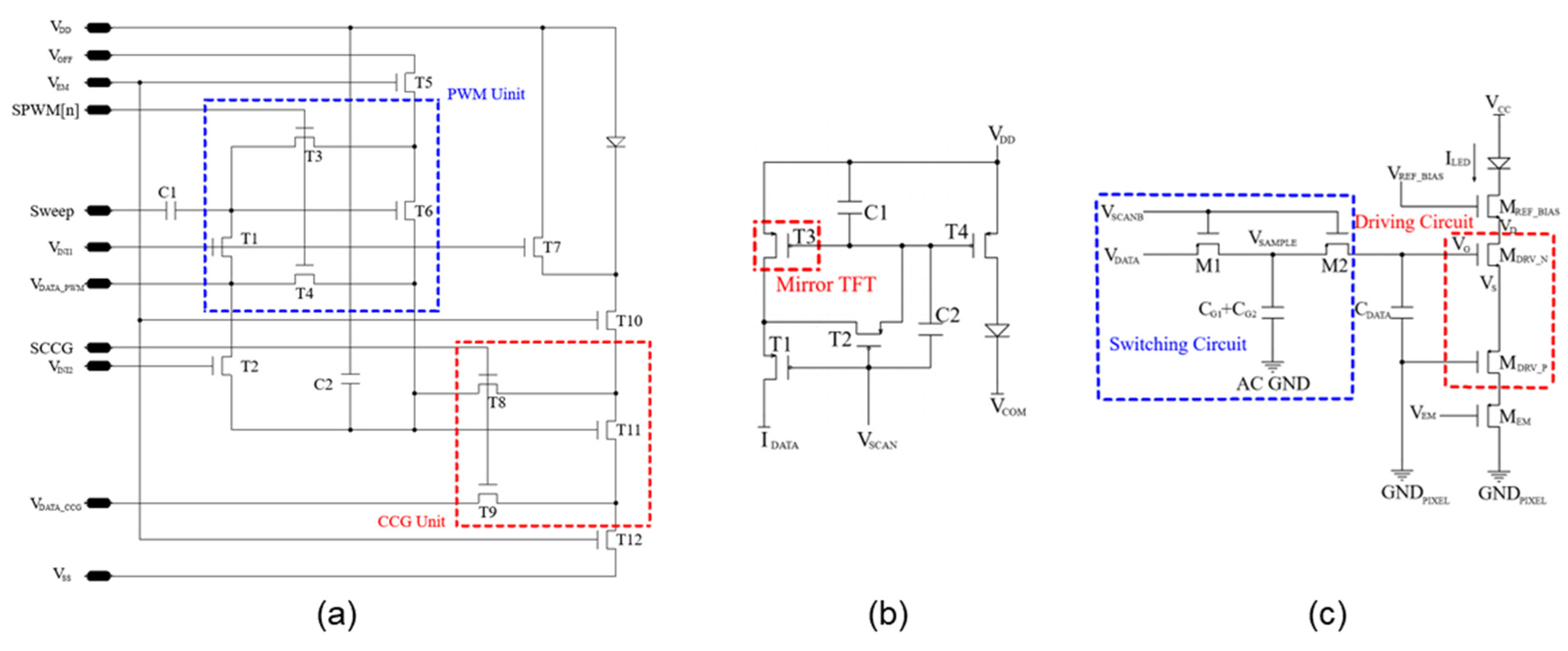
4. Micro-LED Circuit Design

Micro-LED micro-displays are still in the early stages of development and may gradually replace existing display technologies such as silicon-based LCDs or silicon-based OLEDs in certain applications in the future [96]. We compared some pixel circuit design features of glass-based and silicon-based micro-LEDs, as shown in Table 3.

TFT Micro-LED Pixel Circuits

Micro-LEDs and OLEDs are current-driven devices, so the pixel circuits are relatively similar, with the basic 2T1C circuitry. There are two methods to drive micro-LEDs: pulse amplitude modulation (PAM) and pulse width modulation (PWM). PAM directly controls the brightness of micro-LEDs by adjusting the amplitude of the drive current, and its pixel circuit structure is simple, which is conducive to achieving high pixel density. However, due to the high leakage current of the driving transistors, it needs to rely on complex external compensation circuits to maintain voltage stability [21], leading to an increase in system power consumption. PWM indirectly controls the brightness by adjusting the luminous time (duty cycle) at a fixed current, and its pixel circuits usually require more transistors to achieve precise timing control [96]. Despite the higher complexity of PWM’s pixel circuit, its core advantage is to avoid the wavelength shift of the centre of the micro-LEDs caused by current variations, thus solving the problem of colour casting of the display due to PAM [97]. In addition, the external circuit design of PWM varies depending on the implementation: analogue PWM requires the generation of a linearly varying Vsweep signal, while digital PWM requires the generation of EM (enable) signals with different duty cycles via a timing controller, and the overall complexity may be higher than that of the PAM scheme. However, in low-refresh-rate scenarios, PWM can achieve lower power consumption by reducing the switching frequency.
Samsung has solved the problem of wavelength shift in micro-LED displays due to variations in current density by using PAM and PWM driver units with external and internal compensation of VTH, respectively [98]. This circuit is not a PHM (pulse hybrid modulation) drive mode, as mentioned subsequently. The conventional PWM method combined with internal compensation circuitry makes it difficult to achieve high bits. Peng, J. et al. used a 7T1C pixel circuit [99] to improve the bit of a 240 Hz 10-line panel from 3 to 8 bits by converting equal subfields to unequal subfields and combining PWM method and internal compensation. Hong, Y. et al. proposed to combine the constant current generation unit in PAM with the PWM drive as shown in Figure 9a for the 13T3C circuit [100]. Applying PWM drive to the proposed pixel circuit to fix the current density of micro-LEDs similarly improves the problem of wavelength drift at the centre of micro-LEDs. Combining the PWM pixel circuit with the pixel compensation circuit, we provide constant current through analogue VDATA modulation and improve display uniformity by compensating for PWM TFT and driving TFT VTH shift [101]. Zou, P.-A. et al. proposed a new uncompensated analogue PWM pixel circuit [102], which simplified the circuit structure by achieving micro-LED operation at constant current through a pull-up control scheme. The brightness uniformity of the fabricated LED arrays is only 74% due to the fact that the brightness uniformity is affected by factors such as the mobility variation in the driving TFT and IR drop. Kim, J. et al. proposed a new pixel circuit based on LTPO TFTs, which combines the internal VTH compensation and the PWM method. This circuit has a micro-LED current error rate of 3.7% and an emission pulse width error rate of 3.4% at a VTH variation of 0.5 V [38].
Although the PWM solution can better solve the central wavelength shift of micro-LEDs with the current value, its complex pixel circuitry occupies a large pixel area. To improve the PPI of the display, the PAM solution is introduced. Good display uniformity and emission stability can also be achieved using a current control current source (CCCS). Zhang, K. et al. proposed a 4T2C pixel circuit using CCCS [103] (Figure 9b). The circuit uses the principle of current mirroring to make ILED proportional to IDATA (affected by the W/L of T3 and T4). When T1 and T2 are switched off, the voltage stored in the capacitor continuously keeps the T4 switched on, thus providing stable current to the micro-led throughout the entire frame cycle.
The PWM scheme can better solve the centre wavelength shift problem of micro-LEDs, but it has lower brightness control accuracy at high grey levels and may face flickering problem. On the contrary, PAM is able to achieve high-precision brightness control and stability at high grey levels but has poor brightness uniformity and low efficiency at low grey levels. Therefore, the PHM drive mode combines the advantages of PWM and PAM. In low greyscale, PWM mode is used to adjust the light emitting time to keep the micro-LED current at a high and constant level. At a high grey level, the PAM mode is used to improve the brightness control accuracy. Xiao, J. et al. proposed the 11T4C pixel circuit based on the PHM driving mode. The circuit exhibits good brightness uniformity and stability at different grey levels and has good aging resistance [104]. Kim, S.S. et al. connected multiple LED driver circuits in series by daisy-chaining connections based on the PHM driving mode to facilitate the expansion of the LED driver-integrated circuits and to achieve synchronous transmission of clock and data signals [105].
  • Silicon-based micro-LED pixel circuits
MOSFETs, being more mature than TFTs, enable smaller-sized displays and integrated peripheral circuits, making them a suitable solution for micro-displays smaller than 1 inch [106]. MOSFET circuits have unique properties such as low power consumption, high noise immunity, good integration, and stability [107]. Complementary metal oxide semiconductor (CMOS) inverters (i.e., n-type and p-type transistors) can easily reduce the size of the device, place analogue and digital circuits on the same chip, and have low fabrication costs. Some researchers have used NMOS, PMOS, and CMOS to drive micro-LEDs and found that CMOS used to drive micro-LEDs performs the best in terms of switching characteristics and does not suffer from incomplete turn-off [108].
Seong, J. et al. proposed a MOSFET pixel circuit (Figure 9c) for micro-LED using PAM driving, which addresses the leakage current and IR drop problems [96]. For the switching branch, the circuit uses M1 and M2, and CG1 and CG2 to form a “T-switch” structure, where CG1 and CG2 create a VSAMPLE node, which is normally VSAMPLE = VDATA. Delaying the change in VSAMPLE with CG1 and CG2 reduces the difference between VGATE and VSAMPLE. As a result, the VDS of M2 is close to zero, reducing the leakage current of M2. For the driver branch, the combination of the VGS of MDRV_N and MDRV_P determined the bias current of the OLED. By adding MOSFET, the VGS deviation of the driving circuit is made independent of any ground reference, thus effectively suppressing the IR drop problem.
Lee, P.-Y.L. et al. used CMOS technology for the design of micro-LED display drivers with 10-bit current-mode PWM. They improved the driving speed of current-mode PWM by using two switching transistors for PWM control and scanning control, respectively. In addition, the use of PMOS transistors in the pixel circuit effectively prevents current spikes [109]. Cha, P.C.-P. et al. proposed an A-PWM MOSFET pixel circuit aimed at reducing the nonlinearity of the emitted grey level of the micro-LED display, where two transistors and a CMOS component together form an intra-pixel SRAM for stabilising the node voltages and fast switching when needed, thus reducing the rise or fall delay of the micro-LED emission [110].

5. Conclusions

Displays are vital for the development of a digital society. Displays are classified into LCD, OLED, and micro-LED based on their display technologies. Displays are categorised by size into small and medium-sized displays and micro-displays. Small and medium-sized displays are typically driven by glass-based TFT, while micro-displays are usually driven by silicon-based MOSFETs. Glass-based TFTs are categorised into a-Si TFT, LTPS TFT, MO TFT, and LTPO TFT based on their semiconductor materials. In combination with the TFT device structure, TFTs are further divided into traditional single-gate TFTs and newer double-gate TFTs.
Glass-based display technology is widely used in LCDs, OLEDs, and micro-OLEDs. LCDs are voltage-driven devices with relatively low requirements for TFTs. Therefore, a-Si TFTs are mature, inexpensive, and widely used. OLEDs and micro-LEDs are current-driven devices with high requirements for TFTs. To solve problems such as uneven display caused by poor stability, both internal and external compensation circuits have been designed. In addition, circuit structures such as mirror structures, diode-connected transistors, and synchronous emission schemes are combined to achieve low frequency, low power consumption, high resolution displays, etc. The micro-LED driving method is similar to that of OLED. Micro-LEDs adopt driving methods such as a combination of PWM and PAM to solve the problem of colour deviation caused by the shifting of its central wavelength.
Silicon-based display technology is primarily used in micro-OLEDs and micro-LEDs. As pixel size shrinks, the device gradually suffers from decreased efficiency and increased leakage current. Therefore, MOSFETs are commonly used to drive these devices. Micro-OLEDs combine MOSFET with source followers and a capacitive voltage divider to expand the data voltage regulation range of the pixel circuit to ensure the normal work of MOSFETs. Micro-LED adopts a circuit design, such as a “t-switch” structure, to reduce leakage current and achieve low power consumption.
The future display market is promising, with various display technologies gradually becoming subdivided to correspond to different device requirements. For glass-based display technology, new advancements such as LTPO technology have a broad development prospect. However, the major challenge facing LTPO technology is the compatibility with LTPS and MO processes. Silicon-based display technology is constrained by the size limitations of silicon wafer. The main direction of development is to gradually shift from micro sizes to small sizes. The key challenge in this shift lies in cost control.

Author Contributions

Conceptualisation, D.-M.W., H.Z., C.-H.T., W.-J.W., H.N. and B.J.; methodology, D.-M.W. and H.Z.; investigation, D.-M.W., H.Z., C.-H.T., S.Z., M.X., L.W. and B.J.; writing—original draft, D.-M.W., H.Z., C.-H.T. and B.J.; writing—review and editing, D.-M.W., H.Z., C.-H.T., S.Z., H.-D.L., L.Z., Y.C., C.W., M.X., L.W. and B.J.; visualisation, H.Z. and C.-H.T.; project administration, H.Z. and C.-H.T.; funding acquisition, H.Z., M.X. and B.J. All authors have read and agreed to the published version of the manuscript.

Funding

This research was supported in part by the Guangdong Basic and Applied Basic Research Foundation under grant 2021B1515140053; in part by the R&D project in key areas of Dongguan City under grant 20201200300102; in part by the Guangzhou Science and Technology Program under grant 2024B01J0079; and in part by the SSL Science and Technology Commissioner Program under grant 20234368-01KCJ-G.

Data Availability Statement

No new data were created or analyzed in this study.

Conflicts of Interest

The authors declare no conflicts of interest.

References

  1. Chen, H.-W.; Lee, J.-H.; Lin, B.-Y.; Chen, S.; Wu, S.-T. Liquid Crystal Display and Organic Light-Emitting Diode Display: Present Status and Future Perspectives. Light. Sci. Appl. 2018, 7, 17168. [Google Scholar] [CrossRef] [PubMed]
  2. Parbrook, P.J.; Corbett, B.; Han, J.; Seong, T.; Amano, H. Micro-Light Emitting Diode: From Chips to Applications. Laser Photonics Rev. 2021, 15, 2000133. [Google Scholar] [CrossRef]
  3. Wang, I.-S. Dynamic Pixel Models for A-Si TFT-LCD and Their Implementation in SPICE. ETRI J. 2012, 34, 633–636. [Google Scholar] [CrossRef]
  4. Liu, B.; Chen, G.; Cai, X.; Yang, X.; Chen, B.; Zhu, C.; Li, J.; Tseng, C. P-55: Image Flicker Improvement in LTPS TFT-LCD with Low Frequency Driving. SID Symp. Dig. Tech. Pap. 2018, 49, 1403–1406. [Google Scholar] [CrossRef]
  5. Kim, D.; Kim, Y.; Lee, S.; Kang, M.S.; Kim, D.H.; Lee, H. High Resolution A-IGZO TFT Pixel Circuit for Compensating Threshold Voltage Shifts and OLED Degradations. IEEE J. Electron Devices Soc. 2017, 5, 372–377. [Google Scholar] [CrossRef]
  6. Sodhani, A.; Goswami, R.; Kandpal, K. Design of Pixel Circuit Using A-IGZO TFTs to Enhance Uniformity of AMOLED Displays by Threshold Voltage Compensation. Arab. J. Sci. Eng. 2021, 46, 9663–9672. [Google Scholar] [CrossRef]
  7. Bagheri, M.; Cheng, X.; Zhang, J.; Lee, S.; Ashtiani, S.; Nathan, A. Threshold Voltage Compensation Error in Voltage Programmed AMOLED Displays. J. Disp. Technol. 2016, 12, 658–664. [Google Scholar] [CrossRef]
  8. Jankovic, N.D.; Brajovic, V. Vth compensated AMOLED pixel employing dual-gate TFT driver. Electron. Lett. 2011, 47, 456–457. [Google Scholar] [CrossRef]
  9. Lih, J.-J.; Sung, C.-F.; Li, C.-H.; Hsiao, T.-H.; Lee, H.-H. Comparison of A-Si and Poly-Si for AMOLED Displays. J. Soc. Inf. Disp. 2004, 12, 367–371. [Google Scholar] [CrossRef]
  10. Li, Y.-L.; Liu, Y.-T. MicroLED Display: The next-Generation Display Technology. In Proceedings of the Advances in Display Technologies X, San Francisco, CA, USA, 26 February 2020; SPIE: Bellingham, WA, USA, 2000; Volume 11304, pp. 72–75. [Google Scholar]
  11. Zhou, L.; Zheng, H.; Zhang, S.H.; Li, H.D.; Zhang, G.; Zhang, S.Q.; Xu, W.; Xu, H.R.; Xiao, J.L.; Ning, H.L. Advances in Micro-LED Display and Its Driving Technology. Liq. Cryst. Disp. 2022, 37, 1395–1410. [Google Scholar]
  12. Anwar, A.R.; Sajjad, M.T.; Johar, M.A.; Hernández-Gutiérrez, C.A.; Usman, M.; Łepkowski, S.P. Recent Progress in Micro-LED-Based Display Technologies. Laser Photonics Rev. 2022, 16, 2100427. [Google Scholar] [CrossRef]
  13. Luo, Z.; Ding, Y.; Peng, F.; Wei, G.; Wang, Y.; Wu, S.-T. Ultracompact and High-Efficiency Liquid-Crystal-on-Silicon Light Engines for Augmented Reality Glasses. Opto-Electron. Adv. 2024, 7, 240039. [Google Scholar] [CrossRef]
  14. Lin, C.-C.; Wu, Y.-R.; Kuo, H.-C.; Wong, M.S.; DenBaars, S.P.; Nakamura, S.; Pandey, A.; Mi, Z.; Tian, P.; Ohkawa, K.; et al. The Micro-LED Roadmap: Status Quo and Prospects. J. Phys. Photonics 2023, 5, 042502. [Google Scholar]
  15. Advances and Challenges in Microdisplays and Imaging Optics for Virtual Reality and Mixed Reality: Device. Available online: https://www.cell.com/device/abstract/S2666-9986(24)00234-5 (accessed on 20 March 2025).
  16. Hsiang, E.-L.; Yang, Z.; Yang, Q.; Lai, P.-C.; Lin, C.-L.; Wu, S.-T. AR/VR Light Engines: Perspectives and Challenges. Adv. Opt. Photonics 2022, 14, 783. [Google Scholar] [CrossRef]
  17. Yin, K.; Hsiang, E.-L.; Zou, J.; Li, Y.; Yang, Z.; Yang, Q.; Lai, P.-C.; Lin, C.-L.; Wu, S.-T. Advanced Liquid Crystal Devices for Augmented Reality and Virtual Reality Displays: Principles and Applications. Light. Sci. Appl. 2022, 11, 161. [Google Scholar] [CrossRef]
  18. Miao, W.-C.; Hsiao, F.-H.; Sheng, Y.; Lee, T.-Y.; Hong, Y.-H.; Tsai, C.-W.; Chen, H.-L.; Liu, Z.; Lin, C.-L.; Chung, R.-J.; et al. Microdisplays: Mini-LED, Micro-OLED, and Micro-LED. Adv. Opt. Mater. 2024, 12, 2300112. [Google Scholar] [CrossRef]
  19. Hara, Y.; Kikuchi, T.; Kitagawa, H.; Morinaga, J.; Ohgami, H.; Imai, H.; Daitoh, T.; Matsuo, T. IGZO-TFT Technology for Large-Screen 8K Display. J. Soc. Inf. Disp. 2018, 26, 169–177. [Google Scholar] [CrossRef]
  20. Bandari, V.K.; Schmidt, O.G. A Bright Future for Micro-LED Displays. Light. Sci. Appl. 2024, 13, 317. [Google Scholar] [CrossRef]
  21. Xu, H.; Liu, B.; Zheng, F.; Xiao, J.; Zhang, S.; Lu, L. A Compensation Pixel Circuit with High Bits Using PWM Method for AMLED. Energy Rep. 2023, 9, 194–199. [Google Scholar] [CrossRef]
  22. Qi, L.; Zhang, X.; Chong, W.C.; Lau, K.M. Monolithically Integrated High-Resolution Full-Color GaN-on-Si Micro-LED Microdisplay. Photonics Res. PRJ 2023, 11, 109–120. [Google Scholar] [CrossRef]
  23. Wu, M.-C.; Chung, M.-C.; Wu, C.-Y. 3200 Ppi Matrix-Addressable Blue MicroLED Display. Micromachines 2022, 13, 1350. [Google Scholar] [CrossRef] [PubMed]
  24. Hsu, Y.-H.; Lin, Y.-H.; Wu, M.-H.; Kuo, H.C.; Horng, R.-H. Current Confinement Effect on the Performance of Blue Light Micro-LEDs with 10 Μm Dimension. ACS Omega 2023, 8, 35351–35358. [Google Scholar] [CrossRef] [PubMed]
  25. Stewart, M.; Howell, R.S.; Pires, L.; Hatalis, M.K. Polysilicon TFT Technology for Active Matrix OLED Displays. IEEE Trans. Electron Devices 2001, 48, 845–851. [Google Scholar] [CrossRef]
  26. Wu, Y.-E.; Lee, M.-H.; Lin, Y.-C.; Kuo, C.; Lin, Y.-H.; Huang, W.-M. 41-1: Invited Paper: Active Matrix Mini-LED Backlights for 1000PPI VR LCD. Symp. Dig. Tech. Pap. 2019, 50, 562–565. [Google Scholar] [CrossRef]
  27. Koden, M. OLED Displays and Lighting, 1st ed.; Wiley: Hoboken, NJ, USA, 2016; ISBN 978-1-119-04045-3. [Google Scholar]
  28. Zhang, S.; Zheng, H.; Zhou, L.; Li, H.; Chen, Y.; Wei, C.; Wu, T.; Lv, W.; Zhang, G.; Zhang, S.; et al. Research Progress of Micro-LED Display Technology. Crystals 2023, 13, 1001. [Google Scholar] [CrossRef]
  29. Wager, J.F. Flat-Panel-Display Backplanes: LTPS or IGZO for AMLCDs or AMOLED Displays? Inf. Disp. 2014, 30, 26–29. [Google Scholar] [CrossRef]
  30. Wager, J.F. TFT Technology: Advancements and Opportunities for Improvement. Inf. Disp. 2020, 36, 9–13. [Google Scholar] [CrossRef]
  31. Sarma, K.R. Amorphous Silicon: Flexible Backplane and Display Application. In Flexible Electronics: Materials and Applications; Wong, W.S., Salleo, A., Eds.; Springer: Boston, MA, USA, 2009; pp. 75–106. ISBN 978-0-387-74363-9. [Google Scholar]
  32. Nodera, N.; Utsugi, S.; Ishida, S.; Takakura, R.; Matsushima, Y.; Michinaka, S.; Matsumoto, T.; Kobayashi, K.; Oketani, T. Novel LTPS Technology for Large Substrate. J. Soc. Inf. Disp. 2016, 24, 394–401. [Google Scholar] [CrossRef]
  33. Lin, C.-L.; Lai, P.-C.; Shih, L.-W.; Hung, C.-C.; Lai, P.-C.; Lin, T.-Y.; Liu, K.-H.; Wang, T.-H. Compensation Pixel Circuit to Improve Image Quality for Mobile AMOLED Displays. IEEE J. Solid-State Circuits 2019, 54, 489–500. [Google Scholar] [CrossRef]
  34. Fan, C.-L.; Chen, Y.-C.; Yang, C.-C.; Tsai, Y.-K.; Huang, B.-R. Novel LTPS-TFT Pixel Circuit with OLED Luminance Compensation for 3D AMOLED Displays. J. Disp. Technol. 2016, 12, 425–428. [Google Scholar] [CrossRef]
  35. Hosono, H. How We Made the IGZO Transistor. Nat. Electron. 2018, 1, 428. [Google Scholar] [CrossRef]
  36. Yin, X.; Deng, S.; Li, G.; Zhong, W.; Chen, R.; Li, G.; Yeung, F.S.Y.; Wong, M.; Kwok, H.S. Low Leakage Current Vertical Thin-Film Transistors with InSnO-Stabilized ZnO Channel. IEEE Electron Device Lett. 2020, 41, 248–251. [Google Scholar] [CrossRef]
  37. Park, J.H.; Seok, K.H.; Kim, H.Y.; Chae, H.J.; Lee, S.K.; Joo, S.K. A Novel Design of Quasi-Lightly Doped Drain Poly-Si Thin-Film Transistors for Suppression of Kink and Gate-Induced Drain Leakage Current. IEEE Electron Device Lett. 2015, 36, 351–353. [Google Scholar] [CrossRef]
  38. Kim, J.; Lee, H.; Jeong, M.; Bae, J.; Park, C.; Jang, J. Micro-LED Pixel Circuit Using Low-Temperature Poly-Si Oxide TFTs with Fast Rise and Fall Times of Pulse Width Modulation for Low Gray Expression. IEEE Electron Device Lett. 2023, 44, 1448–1451. [Google Scholar] [CrossRef]
  39. Zulqarnain, M.; Cantatore, E. Analog and Mixed Signal Circuit Design Techniques in Flexible Unipolar A-IGZO TFT Technology: Challenges and Recent Trends. IEEE Open J. Circuits Syst. 2021, 2, 743–756. [Google Scholar] [CrossRef]
  40. Chen, C.; Abe, K.; Kumomi, H.; Kanicki, J. A-InGaZnO Thin-Film Transistors for AMOLEDs: Electrical Stability and Pixel-Circuit Simulation. J. Soc. Inf. Disp. 2009, 17, 525. [Google Scholar] [CrossRef]
  41. Zhong, J.; Li, G.; Guo, R.; Ning, H.; Zhang, H.; Fang, Z.; Fu, X.; Wei, X.; Yao, R.; Peng, J. Bilayer Metal Oxide Channel Thin Film Transistor with Flat Interface Based on Smooth Transparent Nanopaper Substrate. IEEE Electron Device Lett. 2022, 43, 2113–2116. [Google Scholar] [CrossRef]
  42. Ning, H.; Zeng, X.; Zhang, H.; Zhang, X.; Yao, R.; Liu, X.; Luo, D.; Xu, Z.; Ye, Q.; Peng, J. Transparent Flexible IGZO Thin Film Transistors Fabricated at Room Temperature. Membranes 2021, 12, 29. [Google Scholar] [CrossRef]
  43. Liang, Z.; Wu, W.; Fu, X.; Ning, H.; Xu, W.; Xiong, X.; Qiu, T.; Luo, C.; Yao, R.; Peng, J. Flexible High-Entropy Poly(Vinyl Alcohol) Dielectric Films Were Prepared at a Low Temperature and Applied to an Indium Gallium Zinc Oxide Thin-Film Transistor. J. Phys. Chem. Lett. 2023, 14, 9245–9249. [Google Scholar] [CrossRef]
  44. Osawa H, Kim K W, Hung M C; et al. Displays with Silicon and Semiconducting Oxide Thin-Film Transistors. U.S. Patent 9,818,765, 14 November 2017.
  45. Chang, T.-K.; Lin, C.-W.; Chang, S. 39-3: Invited Paper: LTPO TFT Technology for AMOLEDs. Symp. Dig. Tech. Pap. 2019, 50, 545–548. [Google Scholar] [CrossRef]
  46. Chung, U.-J.; Choi, S.-C.; Noh, S.Y.; Kim, K.-T.; Moon, K.-J.; Kim, J.-H.; Park, K.-S.; Choi, H.-C.; Kang, I.-B. 15-1: Invited Paper: Manufacturing Technology of LTPO TFT. Symp. Dig. Tech. Pap. 2020, 51, 192–195. [Google Scholar] [CrossRef]
  47. Ye, J.-H.; Huang, C.-L.; Chen, M.-Y.; Hong, H.-Z.; Luo, J.-C.; Huang, K.-Y.; Peng, C.-T.; Chen, M.-S.; Huang, W.-M.; Wu, Y.-A. 12-4: Late-News Paper: Reliability Improvement of IGZO and LTPS Hybrid TFTs Array Technology. Symp. Dig. Tech. Pap. 2018, 49, 128–131. [Google Scholar] [CrossRef]
  48. Luo, C.; Yin, G.; Shu, Z.; Liu, G.; Ai, F. P-2: High-Performance LTPO TFT-LCD Using Metal as Hydrogen Barrier Layer. Symp. Dig. Tech. Pap. 2021, 52, 1063–1066. [Google Scholar] [CrossRef]
  49. Luo, F.C.; Chen, I.; Genovese, F.C. A Thin-Film Transistor for Flat Planel Displays. IEEE Trans. Electron Devices 1981, 28, 740–743. [Google Scholar] [CrossRef]
  50. Xu, Y.; Liu, C.; Amegadez, P.S.K.; Ryu, G.-S.; Wei, H.; Balestra, F.; Ghibaudo, G.; Noh, Y.-Y. On the Origin of Improved Charge Transport in Double-Gate In–Ga–Zn–O Thin-Film Transistors: A Low-Frequency Noise Perspective. IEEE Electron Device Lett. 2015, 36, 1040–1043. [Google Scholar] [CrossRef]
  51. Chen, T.-L.; Huang, K.-C.; Lin, H.-Y.; Chou, C.H.; Lin, H.H.; Liu, C.W. Enhanced Current Drive of Double-Gate $\alpha$-IGZO Thin-Film Transistors. IEEE Electron Device Lett. 2013, 34, 417–419. [Google Scholar] [CrossRef]
  52. Shim, G.W.; Hong, W.; Cha, J.; Park, J.H.; Lee, K.J.; Choi, S. TFT Channel Materials for Display Applications: From Amorphous Silicon to Transition Metal Dichalcogenides. Adv. Mater. 2020, 32, 1907166. [Google Scholar] [CrossRef]
  53. Spijkman, M.; Myny, K.; Smits, E.C.P.; Heremans, P.; Blom, P.W.M.; De Leeuw, D.M. Dual-Gate Thin-Film Transistors, Integrated Circuits and Sensors. Adv. Mater. 2011, 23, 3231–3242. [Google Scholar] [CrossRef]
  54. Jeon, C.; Mativenga, M.; Geng, D.; Jang, J. AMOLED Pixel Circuit Using Dual Gate A-IGZO TFTs for Simple Scheme and High Speed V TH Extraction. SID Symp. Dig. Tech. Pap. 2016, 47, 65–68. [Google Scholar] [CrossRef]
  55. Chen, S.; Hsieh, I.C. Polysilicon TFT Technology Will Solve Problems of Mobility, Pixel Size, Cost, and Yield. Solid State Technol. 1996, 39, 113–118. [Google Scholar]
  56. Ma, R. Active Matrix for OLED Displays. In Handbook of Visual Display Technology; Chen, J., Cranton, W., Fihn, M., Eds.; Springer International Publishing: Cham, Switzerland, 2016; pp. 1821–1841. ISBN 978-3-319-14345-3. [Google Scholar]
  57. Tai, Y.-H.; Chang, C.-Y.; Lin, C.-Y. Design and Simulation of the Pixel Circuit for a 6-in Full HD LTPS TFT LCD Based on the New Digital Driving Method. J. Disp. Technol. 2015, 11, 336–340. [Google Scholar] [CrossRef]
  58. Cao, H.; Tian, C.; Feng, J.; Cheng, H.; Guan, Y.; Liu, G. A Novel Design for a Pixel-Driver Circuit with Boost Function for UWFR Display. SID Symp. Dig. Tech. Pap. 2021, 52, 1085–1087. [Google Scholar] [CrossRef]
  59. Lin, C.-L.; Lai, P.-C.; Chen, F.-H.; Hung, C.-C.; Chen, B.-S. P-17: Novel Pixel Circuit with Inverter Structure Based on a-IGZO TFT for Blue-Phase Liquid Crystal Displays. SID Symp. Dig. Tech. Pap. 2018, 49, 1242–1245. [Google Scholar] [CrossRef]
  60. Jo, J.-H.; Lee, W.-R.; Chung, H.-J.; Lee, S.-W. A Self-Refreshing Memory-in-Pixel Comprising Low Temperature Poly-Silicon and Oxide TFTs for 3-Bit Liquid Crystal Displays. IEEE Electron Device Lett. 2021, 42, 839–842. [Google Scholar] [CrossRef]
  61. Jo, J.-H.; Jeong, W.-B.; Chung, H.-J.; Lee, S.-W. A Self-Refresh Memory-in-Pixel for Low-Power Reflective Liquid Crystal Displays. IEEE Electron Device Lett. 2023, 44, 48–51. [Google Scholar] [CrossRef]
  62. Wang, J.; Nie, C.; Dai, K.; Liao, Y. P-80: 4K Real 240Hz Technology in Large LCD-TFT TVs. SID Symp. Dig. Tech. Pap. 2024, 55, 1688–1690. [Google Scholar] [CrossRef]
  63. Kim, J.; Chung, H.-J.; Lee, S.-W. A Memory-in-Pixel Circuit for Low-Power Liquid Crystal Displays with Low Temperature Poly-Silicon and Oxide Thin Film Transistors. IEEE Electron Device Lett. 2019, 40, 1957–1960. [Google Scholar] [CrossRef]
  64. Kim, J.; Chung, H.-J.; Lee, S.-W. A Low-Power Pixel Circuit Comprising Low-Temperature Poly-Silicon and Oxide TFTs for Liquid Crystal Displays with Panel Self-Refresh Technology. IEEE Electron Device Lett. 2020, 41, 868–871. [Google Scholar] [CrossRef]
  65. Lin, C.-L.; Chang, W.-Y.; Hung, C.-C. Compensating Pixel Circuit Driving AMOLED Display with A-IGZO TFTs. IEEE Electron Device Lett. 2013, 34, 1166–1168. [Google Scholar] [CrossRef]
  66. Sohn, Y.; Moon, G.; Choi, K.; Kim, Y.; Park, K. Effects of TFT Mobility Variation in the Threshold Voltage Compensation Circuit of the OLED Display. J. Inf. Disp. 2017, 18, 25–30. [Google Scholar] [CrossRef]
  67. Mo, Y.G.; Kim, M.; Kang, C.K.; Jeong, J.H.; Park, Y.S.; Choi, C.G.; Kim, H.D.; Kim, S.S. 69.3: Amorphous Oxide TFT Backplane for Large Size AMOLED TVs. Symp. Dig. Tech. Pap. 2010, 41, 1037–1040. [Google Scholar] [CrossRef]
  68. Kim, Y.; Kim, Y.; Lee, H. A Novel P-Type LTPS TFT Pixel Circuit Compensating for Threshold Voltage and Mobility Variations. J. Disp. Technol. 2014, 10, 995–1000. [Google Scholar] [CrossRef]
  69. Zhang, L.; Yu, H.; Xiao, W.; Liu, C.; Chen, J.; Guo, M.; Gao, H.; Liu, B.; Wu, W. Strategies for Applications of Oxide-Based Thin Film Transistors. Electronics 2022, 11, 960. [Google Scholar] [CrossRef]
  70. Shin, H.-J.; Choi, S.-H.; Kim, D.-M.; Han, S.-E.; Bae, S.-J.; Park, S.-K.; Kim, H.-S.; Oh, C.-H. 45-1: A Novel 88-inch 8K OLED Display for Premium Large-Size TVs. Symp. Dig. Tech. Pap. 2021, 52, 611–614. [Google Scholar] [CrossRef]
  71. Dawson, R.M.A.; Shen, Z.; Furst, D.A.; Connor, S.; Hsu, J.; Kane, M.G.; Stewart, R.G.; Ipri, A.; King, C.N.; Green, P.J.; et al. 4.2: Design Ofanlmproved Pixel Fora Polysilicon Active-Matrix Organic LED Display. Symp. Dig. Tech. Pap. 1998, 29, 11–14. [Google Scholar] [CrossRef]
  72. Chung, H.; Kim, Y.-W.; Oh, C.; Kwon, O.-K.; Choi, S.-M. Organic Light Emitting Device Pixel Circuit and Driving Method Therefor. U.S. Patent 7,414,599, 19 August 2008. [Google Scholar]
  73. Lee, J.-H.; Nam, W.-J.; Jung, S.-H.; Han, M.-K. A New Current Scaling Pixel Circuit for AMOLED. IEEE Electron Device Lett. 2004, 25, 280–282. [Google Scholar] [CrossRef]
  74. Nathan, A.; Chaji, G.R.; Ashtiani, S.J. Driving Schemes for A-Si and LTPS AMOLED Displays. J. Disp. Technol. JDT 2005, 1, 267. [Google Scholar]
  75. Lee, G.-H.; Kim, S.-K.; Son, Y.-S.; Jeon, J.-Y.; Jeon, Y.-J.; Cho, G.-H. P-45: A Fast Driving Circuit for AMOLED Displays Using Current Feedback. SID Symp. Dig. 2006, 37, 363. [Google Scholar] [CrossRef]
  76. Lin, C.-L.; Hung, C.-C.; Chen, P.-S.; Lai, P.-C.; Cheng, M.-H. New Voltage-Programmed AMOLED Pixel Circuit to Compensate for Nonuniform Electrical Characteristics of LTPS TFTs and Voltage Drop in Power Line. IEEE Trans. Electron Devices 2014, 61, 2454–2458. [Google Scholar] [CrossRef]
  77. Chu, H.; Wei, N.; Yu, B.; Zhao, H.; Li, Y.; Wang, X.; He, H. A Mirrored 5T1C OLED Pixel Circuit for Compensating Characteristics Variations and Voltage Drop. Microelectron. J. 2023, 131, 105645. [Google Scholar] [CrossRef]
  78. Lin, C.-L.; Lai, P.-C.; Chang, J.-H.; Chen, S.-C.; Tsai, C.-L.; Koa, J.-L.; Cheng, M.-H.; Shih, L.-W.; Hsu, W.-C. Leakage-Prevention Mechanism to Maintain Driving Capability of Compensation Pixel Circuit for Low Frame Rate AMOLED Displays. IEEE Trans. Electron Devices 2021, 68, 2313–2319. [Google Scholar] [CrossRef]
  79. Singh, A.; Goswami, M.; Kandpal, K. Design of a Voltage-programmed V. TH Compensating Pixel Circuit for AMOLED Displays Using Diode-connected a-IGZO TFT. IET Circuits Devices Syst. 2020, 14, 876–880. [Google Scholar] [CrossRef]
  80. Song, E.; Nam, H. Novel Voltage Programming N-Channel TFT Pixel Circuit for Low Power and High Performance AMOLED Displays. Displays 2014, 35, 118–125. [Google Scholar] [CrossRef]
  81. Vosniadis, P.; Siskos, S. A New Threshold-Voltage Compensation Technique of IGZO and LTPS for AMOLED Display Pixel Circuit. In Proceedings of the 2017 Panhellenic Conference on Electronics and Telecommunications (PACET), Xanthi, Greece, 17–18 November 2017; pp. 1–4. [Google Scholar]
  82. Xie, Y.; Chen, P.; Cai, K.; Jia, S.; Yang, C.; Jian, H.; Weng, J. IGZO-TFT Pixel Circuits Compensating Threshold Voltage and Mobility Variations in AMOLED Displays. SID Symp. Dig. Tech. Pap. 2021, 52, 1100–1103. [Google Scholar] [CrossRef]
  83. Kim, J.C.; Lee, I.S.; Kim, H.T.; An, J.B.; Kim, J.S.; Yoo, J.S.; Hwang, H.W.; Choi, H.C.; Ha, Y.M.; Kim, H.J. A Novel LTPO AMOLED Pixel Circuit and Driving Scheme for Variable Refresh Rate. J. Inf. Disp. 2023, 24, 283–298. [Google Scholar] [CrossRef]
  84. Luo, H.; Wang, S.; Kang, J.; Wang, Y.; Zhao, J.; Tsong, T.; Lu, P.; Gupta, A.; Hu, W.; Wu, H.; et al. 24-3: Complementary LTPO Technology, Pixel Circuits and Integrated Gate Drivers for AMOLED Displays Supporting Variable Refresh Rates. Symp. Dig. Tech. Pap. 2020, 51, 351–354. [Google Scholar] [CrossRef]
  85. Luo, H.; Wellenius, P.; Lunardi, L.; Muth, J.F. Transparent IGZO-Based Logic Gates. IEEE Electron Device Lett. 2012, 33, 673–675. [Google Scholar] [CrossRef]
  86. Kang, D.H.; Kang, I.; Ryu, S.H.; Jang, J. Self-Aligned Coplanar a-IGZO TFTs and Application to High-Speed Circuits. IEEE Electron Device Lett. 2011, 32, 1385–1387. [Google Scholar] [CrossRef]
  87. He, X.; Xiao, X.; Deng, W.; Wang, L.; Wang, L.; Chi, S.; Shao, Y.; Chan, M.; Zhang, S. Characteristics of Double-Gate a-IGZO TFT. In Proceedings of the 2014 12th IEEE International Conference on Solid-State and Integrated Circuit Technology (ICSICT), Guilin, China, 28–31 October 2014; pp. 1–3. [Google Scholar]
  88. Li, X.; Geng, D.; Mativenga, M.; Jang, J. High-Speed Dual-Gate a-IGZO TFT-Based Circuits with Top-Gate Offset Structure. IEEE Electron Device Lett. 2014, 35, 461–463. [Google Scholar] [CrossRef]
  89. Lee, J.; Kim, D.; Yang, J.; Moon, K.; Lee, S.; Jeon, J.; Kim, Y.; Choi, S.; Chung, U.; Park, K.; et al. Organic Light-emitting Diode Display Pixel Circuit Employing Double-gate Low-temperature poly-Si Thin-film Transistor and Metal-oxide Thin-film Transistors. J. Soc. Inf. Disp. 2020, 28, 1003–1011. [Google Scholar] [CrossRef]
  90. Bae, J.; Nam, H. Body-Effect-Free OLED-on-Silicon Pixel Circuit Based on Capacitive Division to Extend Data Voltage Range. Electronics 2021, 10, 2351. [Google Scholar] [CrossRef]
  91. Mai, H. Pixel Design and Characterization of High-Performance Tandem OLED Microdisplays; University of Edinburgh: Edinburgh, UK, 2019. [Google Scholar]
  92. Kim, H.; Kwak, B.-C.; Lim, H.-S.; Kwon, O.-K. Pixel Circuit for Organic Light-Emitting Diode-on-Silicon Microdisplays Using the Source Follower Structure. Jpn. J. Appl. Phys. 2010, 49, 03CD05. [Google Scholar] [CrossRef]
  93. Kwak, B.-C.; Lim, H.-S.; Kwon, O.-K. Organic Light-Emitting Diode-on-Silicon Pixel Circuit Using the Source Follower Structure with Active Load for Microdisplays. Jpn. J. Appl. Phys. 2011, 50, 03CC05. [Google Scholar] [CrossRef]
  94. Hong, S.-W.; Kwak, B.-C.; Na, J.-S.; Hong, S.-K.; Kwon, O.-K. Simple Pixel Circuits for High Resolution and High Image Quality Organic Light Emitting Diode-on-Silicon Microdisplays with Wide Data Voltage Range. J. Soc. Inf. Disp. 2016, 24, 110–116. [Google Scholar] [CrossRef]
  95. Na, J.-S.; Hong, S.-K.; Kwon, O.-K. A 4410-Ppi Resolution Pixel Circuit for High Luminance Uniformity of OLEDoS Microdisplays. IEEE J. Electron Devices Soc. 2019, 7, 1026–1032. [Google Scholar] [CrossRef]
  96. Seong, J.; Jang, J.; Lee, J.; Lee, M. CMOS Backplane Pixel Circuit with Leakage and Voltage Drop Compensation for an Micro-LED Display Achieving 5000 PPI or Higher. IEEE Access 2020, 8, 49467–49476. [Google Scholar] [CrossRef]
  97. Kimura, M.; Nishinohara, D.; Nishiyori, T.; Suzuki, D.; Sawamura, S.; Kato, M. Pulse-Width Modulation with Current Uniformization for AM-OLED Micro-Displays on Si LSI Chips. J. Soc. Inf. Disp. 2019, 27, 402–408. [Google Scholar] [CrossRef]
  98. Kim, J.-H.; Shin, S.; Kang, K.; Jung, C.; Jung, Y.; Shigeta, T.; Park, S.-Y.; Lee, H.S.; Min, J.; Oh, J.; et al. 15-1: PWM Pixel Circuit with LTPS TFTs for Micro-LED Displays. Symp. Dig. Tech. Pap. 2019, 50, 192–195. [Google Scholar] [CrossRef]
  99. Zhao, B.; Xiao, J.; Liu, Q.; Liu, B.; Hu, L.; Peng, J. A Novel Compensation Pixel Circuit for High Bits of AM Mini/Micro-LED Based on PWM Method. Energy Rep. 2021, 7, 343–348. [Google Scholar] [CrossRef]
  100. Hong, Y.-H.; Jung, E.K.; Hong, S.; Kim, Y.-S. 61-2: A Novel Micro-LED Pixel Circuit Using N-type LTPS TFT with Pulse Width Modulation Driving. Symp. Dig. Tech. Pap. 2021, 52, 868–871. [Google Scholar] [CrossRef]
  101. Lin, Y.-Z.; Liu, C.; Zhang, J.-H.; Yuan, Y.-K.; Cai, W.; Zhou, L.; Xu, M.; Wang, L.; Wu, W.-J.; Peng, J.-B. Active-Matrix Micro-LED Display Driven by Metal Oxide TFTs Using Digital PWM Method. IEEE Trans. Electron Devices 2021, 68, 5656–5661. [Google Scholar] [CrossRef]
  102. Zou, P.-A.; Xu, Y.-G.; Liu, C.; Zhang, L.-R.; Zhang, J.-H.; Yuan, Y.-K.; Cai, W.; Han, S.-H.; Zhou, L.; Xu, M.; et al. A New Analog PWM Pixel Circuit with Metal Oxide TFTs for Micro-LED Displays. IEEE Trans. Electron Devices 2022, 69, 4306–4311. [Google Scholar] [CrossRef]
  103. Zhang, K.; Liu, Z.; Kwok, H.-S. Current Driving Active Matrix Micro-LED Display. SID Symp. Dig. Tech. Pap. 2018, 49, 272–275. [Google Scholar] [CrossRef]
  104. Xiao, J.; Huo, W.; Yuan, D.; Liang, C.; Lai, G.; Li, J.; Xu, H.; Li, S.; Zhang, S. A New Pixel Circuit for Micro-Light Emitting Diode Displays with Pulse Hybrid Modulation Driving and Compensation. IEEE J. Electron Devices Soc. 2024, 12, 1–6. [Google Scholar] [CrossRef]
  105. Kim, S.S.; Kim, J.S.; Kim, J.H.; Lee, K.R.; Lee, J.M. Led Driving Circuit and Driving Method Thereof. 2023. [Google Scholar]
  106. Ji, X.; Wang, F.; Zhou, H.; Wang, K.; Yin, L.; Zhang, J. 3400 PPI Active-Matrix Monolithic Blue and Green Micro-LED Display. IEEE Trans. Electron Devices 2023, 70, 4689–4693. [Google Scholar] [CrossRef]
  107. Kursun, V.; Friedman, E.G. Multi-Voltage CMOS Circuit Design; John Wiley & Sons: Hoboken, NJ, USA, 2006; ISBN 978-0-470-01024-2. [Google Scholar]
  108. Zhang, X.; Yin, L.; Ren, K.; Zhang, J. Research on Simulation Design of MOS Driver for Micro-LED. Electronics 2022, 11, 2044. [Google Scholar] [CrossRef]
  109. Lee, P.-Y.L.; Li, S.H.; Hung, T.Y.; Yang, Y.-W.; Li, S.-H.; Sun, J.-J.; Lin, C.-W.D.; Lu, C.-W.; Fang, Y.-H.; Kuo, W.-H.; et al. A 10-Bit 1280 × 720 Micro-LED Display Driver with 2-Transistor Pixel Circuits and Current-Mode Pulse Width Modulation. IEEE Solid-State Circuits Lett. 2022, 5, 134–137. [Google Scholar] [CrossRef]
  110. Cheng, S.-S.; Chao, P.C.-P. A New SRAM-Embedded Pixel Circuit That Modulates Accurately Gray Level for PWM-Driven Micro-LED Displays. IEEE Solid-State Circuits Lett. 2023, 6, 157–160. [Google Scholar] [CrossRef]
Figure 1. Passive matrix drive draft (a) and active matrix drive draft (b) [24].
Asi 08 00046 g001
Figure 2. IGZO and LTPS TFT array technology with a metal barrier layer [48].
Asi 08 00046 g002
Figure 3. DG TFT device structure [54].
Asi 08 00046 g003
Figure 4. LCD TFT array.
Asi 08 00046 g004
Figure 5. Digital drive pixel circuit (a) [57], 3T1C pixel circuit with VGS boost function (b) [58], BPLCD pixel circuit (c) [59], multilevel MIP circuit (d) [60], MIP circuit (e) [61].
Asi 08 00046 g005
Figure 8. Source-following pixel circuits (a,b) [92,93] and capacitive voltage divider pixel circuits (c,d) [94,95].
Asi 08 00046 g008
Figure 9. 13T3C pixel circuit (a) [100], 4T2C pixel circuit for CCCS (b) [103], and 6T1C pixel circuit (c) [96].
Asi 08 00046 g009
Table 1. Comparison of direct-view displays and projection near-eye display features.
CategoryDisplay TypePanel Size (Inches)SubstratePPI (Pixels per Inch)Technical Difficulties
Direct-view displaysAM-LCD5–85Glass300–600Backlighting, response speed
AM-OLED400–800Lifetime, screen burn-in
AM-LED2000–7000Massive transfer, full colour
Projection near-eye displaysHigh-resolution density LCD0.5–2.5Glass/
Silicon
800–2000Flickering, small aperture ratio
LCoS (liquid crystal on silicon)0.3–2.5Silicon2000–5000Edge field effect, voltage swing limit
Silicon-based OLED0.4–1.5Silicon3000–5644Manufacturing yield and lifetime
Silicon-based LED0.4–1.5Silicon2000–7000Huge transfers, efficiency degradation, and current congestion
Table 2. Features and applications of a-Si TFT, LTPS TFT, and MO TFT [27].
TFTa-Si TFTLTPS TFTMO TFT
MicrostructureAmorphousPolycrystallineAmorphous
Max process temperature (°C)330500350
CostLowHighLow
Mobility (cm2/Vs)0.1–150–10010–30
PPILowHighHigh
Threshold voltage (VTH) uniformityGoodWorseGood
VTH stabilityWorseGoodBetter
Logic powerWorseBetterGood
ApplicationLCDLCD
OLED
Micro-LED
LCD
OLED
Micro-LED
Table 3. Comparison table of glass-based (TFT) and silicon-based (CMOS) micro-LEDs.
FeatureGlass Substrate (TFT)Silicon Substrate (CMOS)
Substrate characteristicsLow cost
Easy to achieve large sizes
Low carrier mobility
High cost
High integration
High carrier mobility
Circuit complexityLimited circuit design
High demand for compensation circuits
Flexible circuit design
Easy integration of compensation circuits
Compatible driving techniquesSuitable for PWM (easy to implement)
Difficult to implement PAM
Limited implementation of PHM
Suitable for PAM (high-precision control)
Easy to implement PWM (high refresh rate)
Easy to implement PHM (high dynamic range)
Power consumptionHighLow
Manufacturing processCompatible with existing TFT-LCD processes
Lower difficulty in mass transfer
Requires high-precision CMOS processes
High difficulty in mass transfer
CostLowHigh
Disclaimer/Publisher’s Note: The statements, opinions and data contained in all publications are solely those of the individual author(s) and contributor(s) and not of MDPI and/or the editor(s). MDPI and/or the editor(s) disclaim responsibility for any injury to people or property resulting from any ideas, methods, instructions or products referred to in the content.

