Article

APTES-Modified Interface Optimization in PbS Quantum Dot SWIR Photodetectors and Its Influence on Optoelectronic Properties

1
College of Integrated Circuits and Optoelectronic Chips, Shenzhen Technology University, Shenzhen 518118, China
2
School of Materials Science and Engineering, Hubei University, Wuhan 430062, China
3
College of Engineering Physics, and Center for Intense Laser Application Technology, Shenzhen Technology University, Shenzhen 518118, China
*
Authors to whom correspondence should be addressed.
These authors contributed equally to this work.
Colloids Interfaces 2025, 9(4), 49; https://doi.org/10.3390/colloids9040049
Submission received: 29 May 2025 / Revised: 14 July 2025 / Accepted: 21 July 2025 / Published: 22 July 2025
(This article belongs to the Special Issue State of the Art of Colloid and Interface Science in Asia)

Abstract

Lead sulfide colloidal quantum dots (PbS QDs) have demonstrated great potential in short-wave infrared (SWIR) photodetectors due to their tunable bandgap, low cost, and broad spectral response. While significant progress has been made in surface ligand modification and defect state passivation, studies focusing on the interface between QDs and electrodes remain limited, which hinders further improvement in device performance. In this work, we propose an interface engineering strategy based on 3-aminopropyltriethoxysilane (APTES) to enhance the interfacial contact between PbS QD films and ITO interdigitated electrodes, thereby significantly boosting the overall performance of SWIR photodetectors. Experimental results demonstrate that the optimal 0.5 h APTES treatment duration significantly enhances responsivity by achieving balanced interface passivation and charge carrier transport. Moreover, The APTES-modified device exhibits a controllable dark current and faster photo-response under 1310 nm illumination. This interface engineering approach provides an effective pathway for the development of high-performance PbS QD-based SWIR photodetectors, with promising applications in infrared imaging, spectroscopy, and optical communication.
Keywords:
photodetector; PbS; APTES

1. Introduction

Colloidal quantum dots (QDs), particularly lead sulfide (PbS) QDs [1,2,3], owing to their tunable bandgap, simple synthesis process, and low cost, exhibit broad spectral tunability in the short-wave infrared (SWIR) range. They have been widely applied in areas such as infrared detection [4,5,6,7], solar cells [8,9,10], and biomedical sensing [11,12,13]. Among these, PbS QDs are especially prominent in SWIR photodetectors, primarily because of their low cost and solution processability. In addition, their high dielectric constant, long carrier lifetime, and the potential for multiple-exciton generation contribute to enhanced light absorption and carrier collection efficiencies. More importantly, their process compatibility with large-area substrates and monolithic integration with CMOS circuits [14,15] make them ideal for developing high-resolution, low-crosstalk imaging arrays.
Despite these advantages, a major challenge for PbS QD-based photodetectors lies in the poor charge transport between adjacent QDs, primarily due to long insulating ligands such as oleic acid (OA) used during synthesis [16,17]. These long ligands act as tunneling barriers, limiting carrier mobility and reducing device responsivity. To address this, several strategies have been explored. One effective approach involves employing a two-step ligand-exchange method, which reduces the inter-dot spacing and increases the ligand exchange efficiency. This enhancement in charge transfer capability led to a significant 94% improvement in photodetector responsivity [18]. Additionally, optimizing QD synthesis via the perovskite conversion method (PCM) further facilitates charge carrier transport within the device, yielding additional responsivity improvements [19]. However, investigations into the interface between QDs and electrodes remain limited, despite its critical role in further enhancing device performance.
The interaction between silane coupling agents and QDs has been extensively studied [20,21,22]. In this work, we present a novel and effective strategy for enhancing the performance of PbS QD SWIR photodetectors via interfacial engineering using 3-aminopropyltriethoxysilane (APTES). By modifying the surface of ITO interdigitated electrodes with an APTES layer, the interfacial contact and film morphology between the QD layer and the electrode are significantly enhanced [23,24,25,26,27]. This modification promotes more uniform and denser QD films, facilitates charge transport, and suppresses defect-induced recombination. Systematic studies reveal that the APTES treatment duration is a critical parameter: insufficient treatment results in incomplete passivation, whereas excessive treatment introduces additional tunneling barriers and increases series resistance. An optimized treatment time of 0.5 h achieves the best balance between interface passivation and carrier extraction, resulting in markedly improved responsivity and reduced dark current. These findings not only offer a practical solution for optimizing QD-based photodetectors but also provide new insights into interface engineering for next-generation optoelectronic devices.

2. Materials and Methods

2.1. Materials

Lead (II) chloride (PbCl2, ≥99.99%), sublimed sulfur (S, ≥99.5%), and tetrabutylammonium iodide (TBAI, ≥99%) were purchased from Aladdin (Shanghai, China). 3-Aminopropyltriethoxysilane (APTES, 99%), 1-octadecene (ODE, 90.0%, GC), and n-octane (98%) were obtained from Macklin. Oleic acid (OA, 99%), oleylamine (OlAm, C18 content: 80–90%), n-hexane (≥99.5%), ethanol (≥99.5%), and methanol (≥99.9%) were purchased from Energy Chemical (Anqing, China). All chemicals were used as received without further purification.

2.2. Synthesis of PbS QDs

S precursor: In a three-neck flask, 0.16 g (5 mmol) of sulfur (S) was dissolved in 15 mL of oleylamine (OlAm). The flask was subjected to three cycles of evacuation and nitrogen purging. Then, vacuum was slowly applied until no bubbles were observed. When the temperature reached 120 °C, the system was switched to nitrogen atmosphere and heated for 30 min.
Pb precursor: In another three-neck flask, 0.834 g (3 mmol) of lead (II) chloride (PbCl2) and 7.5 mL of OlAm were mixed. The mixture underwent three cycles of evacuation and nitrogen purging and then was slowly evacuated until no bubbles appeared. Once the temperature reached 125 °C, the system was switched to nitrogen and heated for 30 min.
At 120 °C, 2.25 mL of the S-OlAm solution (containing 0.75 mmol of sulfur) was swiftly injected into the Pb precursor solution. The reaction was allowed to proceed for 170 s. After the reaction, 10 mL of n-hexane and 15 mL of ethanol were added to quench the reaction.

2.3. Ligand Exchange of PbS QDs

The product was collected by centrifugation at 3000 rpm for 3 min, and the supernatant was discarded. The precipitated QDs were redispersed in 10 mL of n-hexane, followed by the addition of 1.5 mL of OA. After thorough mixing, 15 mL of ethanol was added, and the mixture was centrifuged at 3000 rpm for 3 min. The precipitate was redispersed in 10 mL of n-hexane and then reprecipitated with 15 mL of ethanol and centrifuged again at 3000 rpm for 3 min. This washing process was repeated twice. Finally, the precipitate was dried under vacuum for 10 min and stored [28,29].

2.4. Preparation of APTES-Modified SWIR Photodetectors
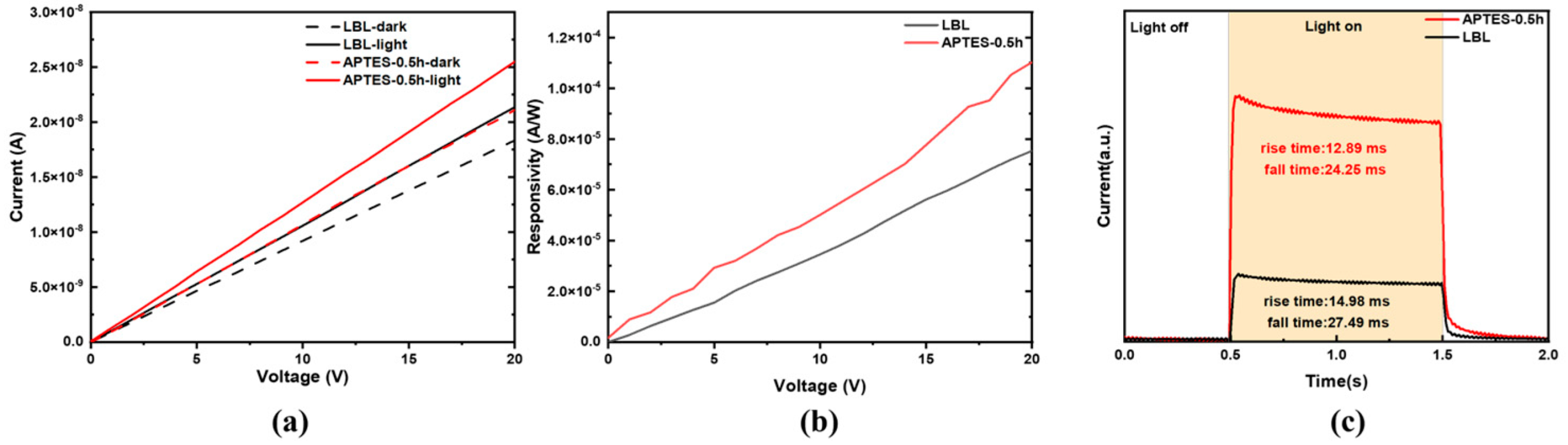
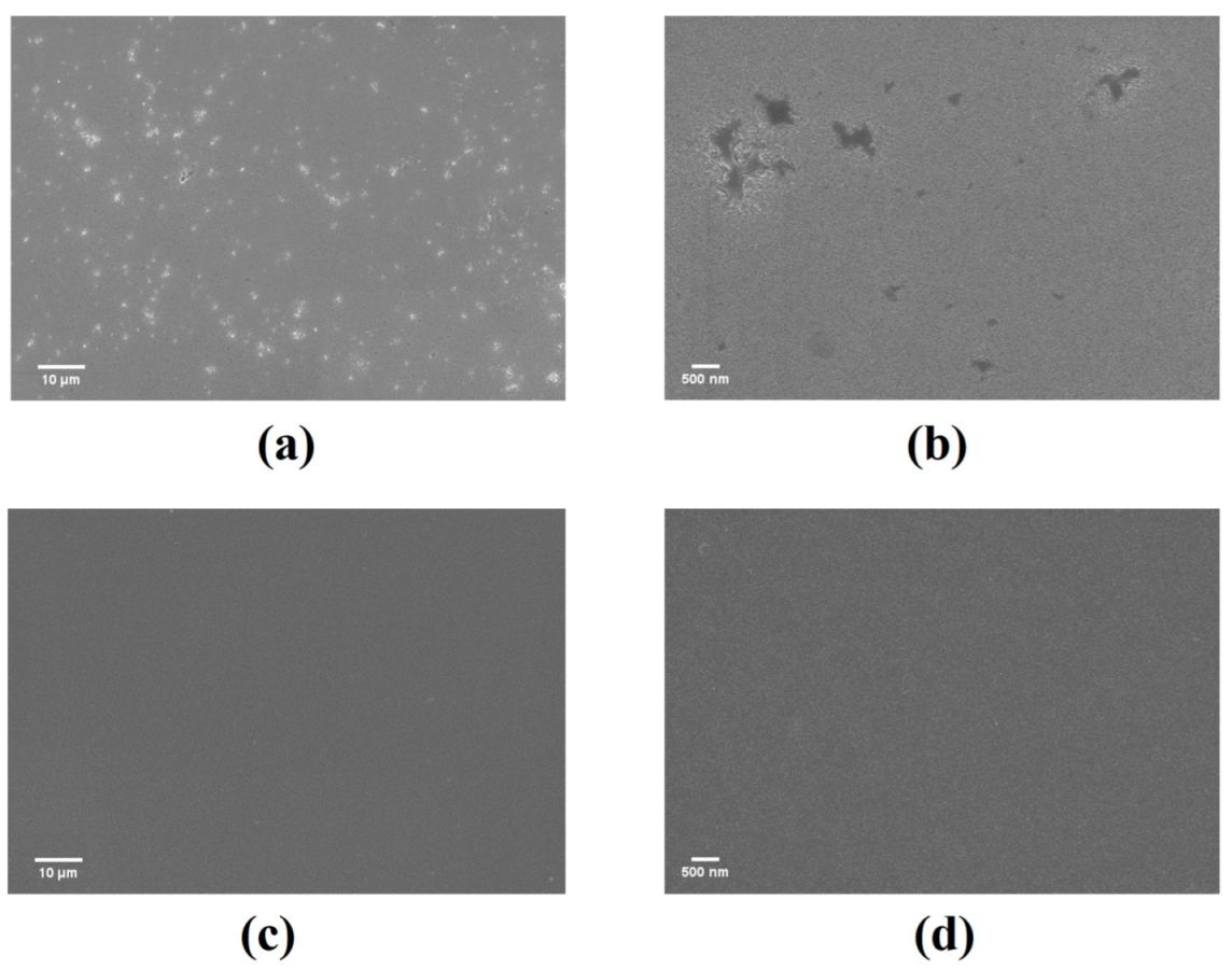
APTES precursor: A 0.05 M APTES solution in n-hexane was prepared by mixing 217.5 μL of APTES with 49.7825 mL of n-hexane to make a total volume of 50 mL.
PbS QDs stock solution: PbS QDs were dispersed in n-octane to obtain a concentration of 50 mg/mL. The resulting solution was filtered twice through a 0.25 μm polytetrafluoroethylene (PTFE) membrane to ensure uniformity and purity.
ITO substrate cleaning: ITO substrates were cleaned using a glass cleaner diluted with water (1:4, v/v), followed by sequential ultrasonication in deionized water, isopropanol, acetone, and ethanol for 20 min each. After cleaning, the substrates were treated with ozone for 15 min to remove any residual organic contaminants.
APTES modification of electrodes: ITO interdigitated electrodes were immersed into the APTES precursor solution for a defined period and then rinsed thoroughly with n-hexane to remove unbound APTES. The immersion time was varied to control the degree of functionalization and thereby tune the interaction between the electrode surface and the PbS QDs.
QDs layer deposition: The 50 mg/mL PbS QD stock solution in n-octane was spin-coated onto the substrate at 3000 rpm for 30 s to form the QD film. A 10 mg/mL solution of tetrabutylammonium iodide (TBAI) in methanol was then drop-cast onto the film and allowed to sit for 30 s. This was followed by spin-coating at 4000 rpm for 10 s. Methanol was applied with a pipette to fully cover the surface, followed by spin-coating at 4000 rpm for another 10 s. The methanol washing step was repeated three times. Steps involving QD deposition, TBAI treatment, and washing were repeated five times to build up the desired multilayer structure. Finally, the device was annealed at 85 °C for 10 min.

3. Results

In this study, APTES was employed as an interfacial modification layer on ITO interdigitated electrodes to enhance the interaction between PbS QDs and the electrode surface, thereby addressing the gap in interface engineering for high-performance PbS QD-based SWIR photodetectors. As illustrated in Figure 1a, an APTES activation layer was introduced at the interface between the PbS QDs and the ITO electrodes. This modification aims to systematically investigate how changes at the interface affect the overall performance of the photodetector.
Figure 1b presents a schematic diagram of the APTES-modified electrodes, highlighting the uniform coverage of the silane layer on the electrode surface. The modification process, detailed in Figure 1b, involves the covalent binding of APTES molecules onto the ITO surface via hydrolysis and condensation reactions, resulting in the formation of siloxane (Si-O-Si) bonds. This treatment exposes surface amino groups (-NH2), which are given the chance to influence the surface chemistry and physical properties of the ITO electrodes. The presence of these amino groups provides an opportunity to enhance adhesion and promote a more uniform deposition of the PbS QD film compared to unmodified electrodes, offering a promising strategy to achieve a denser and more compact QD layer. This improvement in the QD film plays a vital role in promoting efficient charge transport while reducing carrier recombination losses, ultimately contributing to the enhanced performance of optoelectronic devices.
To validate this hypothesis, PbS QDs with a first excitonic absorption peak at 1270 nm were selected as the model system due to their well-defined optical properties in the short-wave infrared (SWIR) region. These QDs were employed as the photosensitive layer of the photodetector to investigate the impact of interfacial engineering on device performance. Figure 2 presents the TEM image and absorption spectrum of these QDs. As shown in Figure 2a,b, the PbS QDs are uniformly dispersed with an average diameter of 3.6 nm. Figure 2c shows the absorption spectrum of the QDs, featuring a sharp and well-defined first excitonic peak centered at 1270 nm. This peak is indicative of strong quantum confinement effects [30,31], which arise when the QD size approaches or falls below the exciton Bohr radius of bulk PbS. The distinct absorption behavior confirms that the QDs possess a bandgap well-suited for SWIR photodetection, making them promising candidates for high-performance optoelectronic applications such as photodetectors and image sensors.
We systematically investigated the impact of APTES introduction on the performance of PbS QD-based photodetectors. As illustrated in Figure 3, the ITO interdigitated electrodes were immersed in the APTES precursor solution for 0.5 h, and the resulting devices were compared with untreated counterparts. A comparison of the I–V characteristics (Figure 3a) reveals that the introduction of APTES creates a more favorable interfacial potential gradient, promoting more efficient separation and transport of photogenerated electron–hole pairs. This improvement is attributed to more efficient separation of photogenerated carriers, likely resulting from the formation of a denser and more uniform PbS QD film on the modified electrode surface. Furthermore, the responsivity–voltage (R–V) curves (Figure 3b) show a consistent increase in responsivity across the measured voltage range, further confirming the positive effect of the APTES layer in facilitating carrier transport. The on/off ratio (Figure 3c) analysis reveals that the LBL device exhibits a rise time of 14.98 ms and a fall time of 27.49 ms, while the APTES-treated device shows a rise time of 12.89 ms and a fall time of 24.25 ms. The results reflect that devices with an APTES duration of 0.5 h have a stronger response and faster response speed. This conclusion is further supported by the SEM analysis shown in Figure 4. In the unmodified device (Figure 4a,b), the PbS QD film exhibits a rough and granular surface morphology, characterized by irregular protrusions and visible voids. In contrast, the APTES-modified sample (Figure 4c,d) presents a significantly smoother and denser morphology. The grain boundaries become less distinct, and the porosity is markedly reduced. Concurrently, AFM analysis provides further evidence: (a) the unmodified device (Figure 5a) exhibits a higher friction force on the PbS QD film, while (b) the APTES-modified device (Figure 5b) shows reduced surface friction. This indicates that the smoothed surface post-modification suppresses carrier scattering, improves interfacial contact, and ultimately enhances device performance. These morphological improvements are indicative of enhanced film quality, which is critical for efficient charge transport in photodetector applications.
The introduction of an APTES interfacial layer plays a pivotal role in tailoring the surface properties of ITO interdigitated electrodes, thereby improving the morphology and performance of PbS QD films. Contact angle measurements provide clear evidence of this surface modification: the water contact angle increased from 71° on bare ITO electrodes to 76° after APTES treatment. This subtle increase is attributed to the exposure of amino groups (-NH2), which exhibit slightly higher hydrophobicity compared to the hydroxyl groups present on the untreated surface. The formation of siloxane bonds (Si-O-Si) via hydrolysis and condensation during the APTES modification process leads to the stable integration of these functional groups (Figure 1b). This change in surface wettability significantly affects the deposition behavior of the PbS QD film. Since these QDs are dispersed in a hydrophobic solvent such as n-octane and are capped with long-chain organic ligands (e.g., OA and OlAm), the enhanced hydrophobicity of the APTES-modified surface improves compatibility and adhesion between the QDs and the substrate. According to the principle of “like dissolves like”, this improved surface match promotes the formation of a more uniform and compact film with reduced porosity and fewer defects. Figure 6a–c systematically investigate the effect of APTES modification time on the performance of PbS QDs photodetectors. By comparing devices fabricated under different soaking durations (0 h, 0.25 h, 0.5 h, 1 h, and 1.5 h), the current–voltage (I–V) characteristics under dark and 1310 nm monochromatic laser illumination, as well as the responsivity–voltage (R–V) curves, reveal the modulation mechanism of device performance by APTES interfacial modification.
The results show that device performance exhibits a “rise then fall” trend as the APTES treatment time increases. At the initial stage, when the soaking time extends from 0 h to 0.25 h, the amino group density on the electrode surface increases, effectively passivating some interface defects, resulting in a significant reduction in dark current. Further extending the soaking time to 0.5 h leads to the formation of a dense and continuous silane layer, which improves the compactness and uniformity of the PbS QD film as well as the interface contact with the electrode. This greatly enhances the separation and collection efficiency of photogenerated carriers. During this stage, the device light current is significantly enhanced, and the responsivity correspondingly increases, with the 0.5 h treated sample exhibiting the best photo-response and overall device performance (Table 1). When combined with the detectivity (D*) results [19], the 0.5 h APTES treatment effectively enhances the D* improvement, strongly supporting the synergistic contributions of effective interfacial defect passivation and enhanced film densification. However, when the treatment time is further extended to 1 h and 1.5 h, the excessively thick silane layer may introduce additional tunneling barriers and increase the device’s series resistance, thereby inhibiting carrier injection and transport. As a result, both light current and responsivity decline to varying degrees. This indicates that the effectiveness of APTES modification is highly sensitive to treatment duration; moderate modification optimizes interface quality and improves device performance, while excessive modification may cause adverse effects, hindering further enhancement. Therefore, precise control of APTES treatment time is crucial for achieving high-performance PbS QD photodetectors. These findings underscore the critical role of interface engineering in optimizing the performance of quantum dot-based optoelectronic devices.

4. Conclusions

In summary, we propose an effective strategy for enhancing the performance of SWIR photodetectors through the APTES surface modification of ITO interdigitated electrodes. This modification significantly improves the interface between the QD film and the electrode, resulting in a denser and smoother film morphology. Such improvements are essential for promoting efficient carrier transport, minimizing recombination losses, and enabling stable, high-performance device operation. Notably, the APTES treatment time is a key parameter in the simultaneous optimization of current and responsivity. Insufficient modification leads to incomplete defect passivation, while excessive treatment introduces additional tunneling barriers and increases series resistance due to a thicker organic layer—both of which degrade device performance [33,34,35]. A 0.5 h treatment strikes the optimal balance, maximizing interfacial passivation and carrier transport. This optimized modification window provides a valuable reference for future device engineering. Further performance improvements may be achieved by combining interfacial energy level alignment or hybrid organic–inorganic dual-modification strategies, unlocking the full potential of PbS QD-based SWIR photodetectors for high-sensitivity, low-noise optoelectronic applications.

Author Contributions

Conceptualization, supervision, project administration, funding acquisition, J.H., J.C. and H.T.; methodology, investigation, Q.L., X.A. and F.F.; formal analysis, data curation, L.R. and W.D., writing—original draft preparation, Q.L. and H.T.; writing—review and editing, J.H. and W.C. All authors have read and agreed to the published version of the manuscript.

Funding

This research was funded by the National Natural Science Foundation of China (No. 62204107), Shenzhen Science and Technology Program (No. JCYJ20240813113240052, JCYJ20241202124709012), Project of Engineering Technology Center of General Universities of Guangdong province (No. 2023GCZX005), Pingshan District Innovation Platform Project of Shenzhen Hi-tech Zone Development Special Plan in 2022 (No. 29853M-KCJ-2023-002-01), and Natural Science Foundation of Top Talent of SZTU (grant no. GDRC202344, GDRC202345).

Data Availability Statement

The original contributions presented in the study are included in the article; further inquiries can be directed to the corresponding authors.

Acknowledgments

The author is grateful to the staff of the Analysis and Testing Center of Shenzhen Technology University for the TEM and absorption spectroscopy analysis.

Conflicts of Interest

The authors declare no conflicts of interest.

References

  1. Moreels, I.; Justo, Y.; De Geyter, B.; Haustraete, K.; Martins, J.C.; Hens, Z. Size-Tunable, Bright, and Stable PbS Quantum Dots: A Surface Chemistry Study. ACS Nano 2011, 5, 2004–2012. [Google Scholar] [CrossRef] [PubMed]
  2. Weidman, M.C.; Beck, M.E.; Hoffman, R.S.; Prins, F.; Tisdale, W.A. Monodisperse, Air-Stable PbS Nanocrystals via Precursor Stoichiometry Control. ACS Nano 2014, 8, 6363–6371. [Google Scholar] [CrossRef] [PubMed]
  3. Wang, Z.; Gu, Y.; Li, X.; Liu, Y.; Liu, F.; Wu, W. Recent Progress of Quantum Dot Infrared Photodetectors. Adv. Opt. Mater. 2023, 11, 2300970. [Google Scholar] [CrossRef]
  4. Zaini, M.S.; Liew, J.Y.C.; Alang Ahmad, S.A.; Mohmad, A.R.; Ahmad Kamarudin, M. Photoluminescence investigation of carrier localization in colloidal PbS and PbS/MnS quantum dots. ACS Omega 2020, 5, 30956–30962. [Google Scholar] [CrossRef] [PubMed]
  5. Venettacci, C.; Martín-García, B.; Prato, M.; Moreels, I.; De Iacovo, A. Increasing responsivity and air stability of PbS colloidal quantum dot photoconductors with iodine surface ligands. Nanotechnology 2019, 30, 405204. [Google Scholar] [CrossRef] [PubMed]
  6. Shrestha, A.; Batmunkh, M.; Tricoli, A.; Qiao, S.Z.; Dai, S. Near-Infrared Active Lead Chalcogenide Quantum Dots: Preparation, Post-Synthesis Ligand Exchange, and Applications in Solar Cells. Angew. Chem. Int. Ed. 2019, 58, 5202–5224. [Google Scholar] [CrossRef] [PubMed]
  7. Pradhan, S.; Di Stasio, F.; Bi, Y.; Gupta, S.; Christodoulou, S.; Stavrinadis, A.; Konstantatos, G. High-efficiency colloidal quantum dot infrared light-emitting diodes via engineering at the supra-nanocrystalline level. Nat. Nanotechnol. 2019, 14, 72–79. [Google Scholar] [CrossRef] [PubMed]
  8. Yang, X.; Yang, J.; Khan, J.; Deng, H.; Yuan, S.; Zhang, J.; Xia, Y.; Deng, F.; Zhou, X.; Umar, F.; et al. Hydroiodic Acid Additive Enhanced the Performance and Stability of PbS-QDs Solar Cells via Suppressing Hydroxyl Ligand. Nano-Micro Lett. 2020, 12, 37. [Google Scholar] [CrossRef] [PubMed]
  9. Tavakoli Dastjerdi, H.; Tavakoli, R.; Yadav, P.; Prochowicz, D.; Saliba, M.; Tavakoli, M.M. Oxygen plasma-induced p-type doping improves performance and stability of PbS quantum dot solar cells. ACS Appl. Mater. Interfaces 2019, 11, 26047–26052. [Google Scholar] [CrossRef] [PubMed]
  10. Chen, W.; Guo, R.; Tang, H.; Wienhold, K.S.; Li, N.; Jiang, Z.; Tang, J.; Jiang, X.; Kreuzer, L.P.; Liu, H.; et al. Operando structure degradation study of PbS quantum dot solar cells. Energy Environ. Sci. 2021, 14, 3420–3429. [Google Scholar] [CrossRef]
  11. Imamura, Y.; Yamada, S.; Tsuboi, S.; Nakane, Y.; Tsukasaki, Y.; Komatsuzaki, A.; Jin, T. Near-infrared emitting PbS quantum dots for in vivo fluorescence imaging of the thrombotic state in septic mouse brain. Molecules 2016, 21, 1080. [Google Scholar] [CrossRef] [PubMed]
  12. Benayas, A.; Ren, F.; Carrasco, E.; Marzal, V.; del Rosal, B.; Gonfa, B.A.; Juarranz, Á.; Sanz-Rodríguez, F.; Jaque, D.; García-Solé, J.; et al. PbS/CdS/ZnS Quantum Dots: A Multifunctional Platform for In Vivo Near-Infrared Low-Dose Fluorescence Imaging. Adv. Funct. Mater. 2015, 25, 6650–6659. [Google Scholar] [CrossRef]
  13. Zebibula, A.; Alifu, N.; Xia, L.; Sun, C.; Yu, X.; Xue, D.; Liu, L.; Li, G.; Qian, J. Ultrastable and Biocompatible NIR-II Quantum Dots for Functional Bioimaging. Adv. Funct. Mater. 2018, 28, 1703451. [Google Scholar] [CrossRef]
  14. Pejović, V.; Georgitzikis, E.; Lee, J.; Lieberman, I.; Cheyns, D.; Heremans, P.; Malinowski, P.E. Infrared Colloidal Quantum Dot Image Sensors. IEEE Trans. Electron Devices 2022, 69, 2840–2850. [Google Scholar] [CrossRef]
  15. Georgitzikis, E.; Malinowski, P.E.; Li, Y.; Maes, J.; Hagelsieb, L.M.; Guerrieri, S.; Hens, Z.; Heremans, P.; Cheyns, D. Integration of PbS Quantum Dot Photodiodes on Silicon for NIR Imaging. IEEE Sens. J. 2020, 20, 6841–6848. [Google Scholar] [CrossRef]
  16. Baranov, D.; Lynch, M.J.; Curtis, A.C.; Carollo, A.R.; Douglass, C.R.; Mateo-Tejada, A.M.; Jonas, D.M. Purification of Oleylamine for Materials Synthesis and Spectroscopic Diagnostics for trans Isomers. Chem. Mater. 2019, 31, 1223–1230. [Google Scholar] [CrossRef]
  17. Chen, S.; Zhong, H.; Wang, X.; Pan, G.; Tang, H.; Fang, F.; Wu, J.; Wang, W.; Xu, L.; Tang, J.; et al. Hybrid-Size Quantum Dots in Hole Transport Layer Depress Dark Current Density of Short-Wave Infrared Photodetectors. ACS Photonics 2025, 12, 879–888. [Google Scholar] [CrossRef]
  18. Tang, H.; Zhong, J.; Chen, W.; Shi, K.; Mei, G.; Zhang, Y.; Wen, Z.; Müller-Buschbaum, P.; Wu, D.; Wang, K.; et al. Lead Sulfide Quantum Dot Photodetector with Enhanced Responsivity through a Two-Step Ligand-Exchange Method. ACS Appl. Nano Mater. 2019, 2, 6135–6143. [Google Scholar] [CrossRef]
  19. Zhang, W.; Fang, F.; Zhong, H.; Huang, L.; Tang, H.; Chen, X.; Hao, J.; Zhang, L.; Cao, L.; Tang, J.; et al. Converting Perovskite Nanocrystals to PbS Quantum Dots Toward Short-Wave Infrared Photodetectors. Adv. Opt. Mater. 2025, 13, 2402740. [Google Scholar] [CrossRef]
  20. Chen, C.; Ao, L.; Wu, Y.T.; Cifliku, V.; Cardoso Dos Santos, M.; Bourrier, E.; Delbianco, M.; Parker, D.; Zwier, J.M.; Huang, L.; et al. Single-Nanoparticle Cell Barcoding by Tunable FRET from Lanthanides to Quantum Dots. Angew. Chem. Int. Ed. 2018, 57, 13686–13690. [Google Scholar] [CrossRef] [PubMed]
  21. Pietra, F.; van Dijk-Moes, R.J.A.; Ke, X.; Bals, S.; Van Tendeloo, G.; de Mello Donega, C.; Vanmaekelbergh, D. Synthesis of Highly Luminescent Silica-Coated CdSe/CdS Nanorods. Chem. Mater. 2013, 25, 3427–3434. [Google Scholar] [CrossRef]
  22. Koole, R.; Van Schooneveld, M.M.; Hilhorst, J.; de Mello Donegá, C.; Hart, D.C.; Van Blaaderen, A.; Vanmaekelbergh, D.; Meijerink, A. On the incorporation mechanism of hydrophobic quantum dots in silica spheres by a reverse microemulsion method. Chem. Mater. 2008, 20, 2503–2512. [Google Scholar] [CrossRef]
  23. Huang, P.Y.; Zhang, Y.Y.; Tsai, P.C.; Chung, R.J.; Tsai, Y.T.; Leung, M.K.; Lin, S.Y.; Fang, M.H. Interfacial Engineering of Quantum Dots–Metal–Organic Framework Composite Toward Efficient Charge Transport for a Short-Wave Infrared Photodetector. Adv. Opt. Mater. 2024, 12, 2302062. [Google Scholar] [CrossRef]
  24. Wu, Z.; Ou, Y.; Cai, M.; Wang, Y.; Tang, R.; Xia, Y. Short-wave infrared photodetectors and imaging sensors based on lead chalcogenide colloidal quantum dots. Adv. Opt. Mater. 2023, 11, 2201577. [Google Scholar] [CrossRef]
  25. Xu, K.; Zhou, W.; Ning, Z. Integrated structure and device engineering for high performance and scalable quantum dot infrared photodetectors. Small 2020, 16, 2003397. [Google Scholar] [CrossRef] [PubMed]
  26. Yin, X.; Zhang, C.; Guo, Y.; Yang, Y.; Xing, Y.; Que, W. PbS QD-based photodetectors: Future-oriented near-infrared detection technology. J. Mater. Chem. C 2021, 9, 417–438. [Google Scholar] [CrossRef]
  27. Yuan, Y.; Xu, J.-L.; Zhang, J.-Y.; Gao, X.; Zhong, Y.-N.; Wang, S.-D. Interface engineering for high photoresponse in PbS quantum-dot short-wavelength infrared photodiodes. IEEE Electron Device Lett. 2022, 43, 1275–1278. [Google Scholar] [CrossRef]
  28. Hines, M.A.; Scholes, G.D. Colloidal PbS Nanocrystals with Size-Tunable Near-Infrared Emission: Observation of Post-Synthesis Self-Narrowing of the Particle Size Distribution. Adv. Mater. 2003, 15, 1844–1849. [Google Scholar] [CrossRef]
  29. Cao; Banin, U. Growth and properties of semiconductor core/shell nanocrystals with InAs cores. J. Am. Chem. Soc. 2000, 122, 9692–9702. [Google Scholar] [CrossRef]
  30. Luther, J.M.; Zheng, H.; Sadtler, B.; Alivisatos, A.P. Synthesis of PbS nanorods and other ionic nanocrystals of complex morphology by sequential cation exchange reactions. J. Am. Chem. Soc. 2009, 131, 16851–16857. [Google Scholar] [CrossRef] [PubMed]
  31. Reiss, P.; Protiere, M.; Li, L. Core/shell semiconductor nanocrystals. Small 2009, 5, 154–168. [Google Scholar] [CrossRef] [PubMed]
  32. Saran, R.; Curry, R.J. Lead sulphide nanocrystal photodetector technologies. Nat. Photonics 2016, 10, 81–92. [Google Scholar] [CrossRef]
  33. Saengdee, P.; Promptmas, C.; Thanapitak, S.; Srisuwan, A.; Pankiew, A.; Thornyanadacha, N.; Chaisriratanakul, W.; Chaowicharat, E.; Jeamsaksiri, W. Optimization of 3-aminopropyltriethoxysilane functionalization on silicon nitride surface for biomolecule immobilization. Talanta 2020, 207, 120305. [Google Scholar] [CrossRef] [PubMed]
  34. Kim, J.; Seidler, P.; Wan, L.S.; Fill, C. Formation, structure, and reactivity of amino-terminated organic films on silicon substrates. J. Colloid Interface Sci. 2009, 329, 114–119. [Google Scholar] [CrossRef] [PubMed]
  35. Howarter, J.A.; Youngblood, J.P. Optimization of Silica Silanization by 3-Aminopropyltriethoxysilane. Langmuir 2006, 22, 11142–11147. [Google Scholar] [CrossRef] [PubMed]
Figure 1. (a) Schematic structure of the SWIR photodetector device on ITO interdigitated electrode substrate; (b) illustration of the APTES optimization process.
Colloids 09 00049 g001
Figure 2. (a) TEM image of PbS QDs, scale bar: 10 nm; (b) size distribution histogram from TEM, average diameter: 3.6 nm; (c) absorption spectrum of PbS QDs.
Colloids 09 00049 g002
Figure 3. Comparison of devices with and without APTES modification: (a) dark and light current; (b) responsivity, and (c) on/off ratio. Measurements were conducted under illumination with a 1310 nm near-infrared laser.
Colloids 09 00049 g003
Figure 4. Comparison of SEM images: (a,b) unmodified devices vs. (c,d) APTES-modified devices. Scale bars: 10 μm (a,c); 500 nm (b,d).
Colloids 09 00049 g004
Figure 5. AFM images comparing devices without (a) and with (b) APTES surface modification.
Colloids 09 00049 g005
Figure 6. Comparison of device performance with different APTES modification durations: (a) dark current; (b) light current; (c) responsivity. Measurements were conducted under illumination with a 1310 nm near-infrared laser.
Colloids 09 00049 g006
Table 1. Comparison of device performance with different APTES modification durations 1.
Time (h)Dark Current (A)Light Current (A)Responsivity(A/W)
01.83 × 10−82.13 × 10−87.54 × 10⁻⁵
0.254.97 × 10−85.37 × 10−81.01 × 10−4
0.52.11 × 10−82.55 × 10−81.10 × 10−4
1.02.70 × 10−83.10 × 10−81.00 × 10−4
1.52.07 × 10−85.91 × 10−89.57 × 10−5
1 At 20V and 1310 nm, the light intensity measured by the power meter is 0.834 mW; the working area of the optical power meter is 94.09 mm2; and the optical power density is 0.89 mW/cm2. The area of the photodetector is 4.5 mm2 [32].
Disclaimer/Publisher’s Note: The statements, opinions and data contained in all publications are solely those of the individual author(s) and contributor(s) and not of MDPI and/or the editor(s). MDPI and/or the editor(s) disclaim responsibility for any injury to people or property resulting from any ideas, methods, instructions or products referred to in the content.

