
The Shape Modulation of Laser-Induced Nanowelded Microstructures Using Two Colors

 , , and
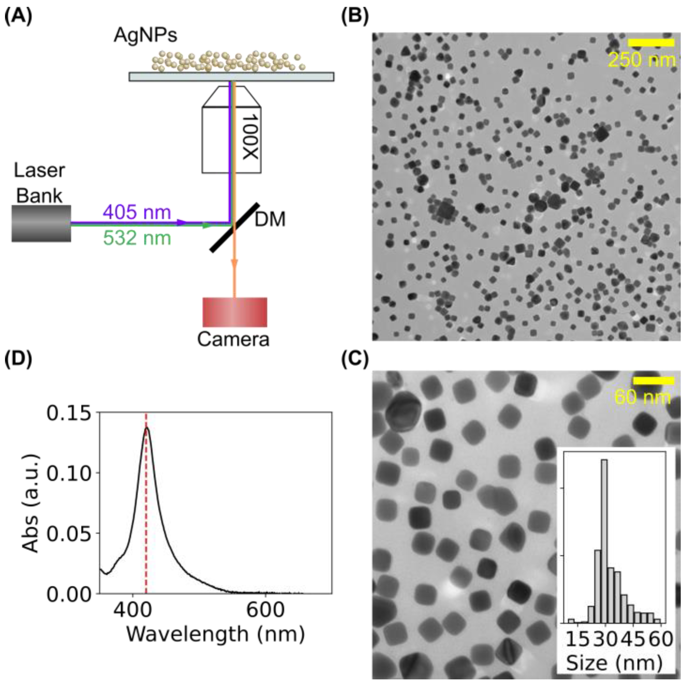
Abstract
1. Introduction
2. Materials and Methods
2.1. Synthesis and Characterization of AgNPs
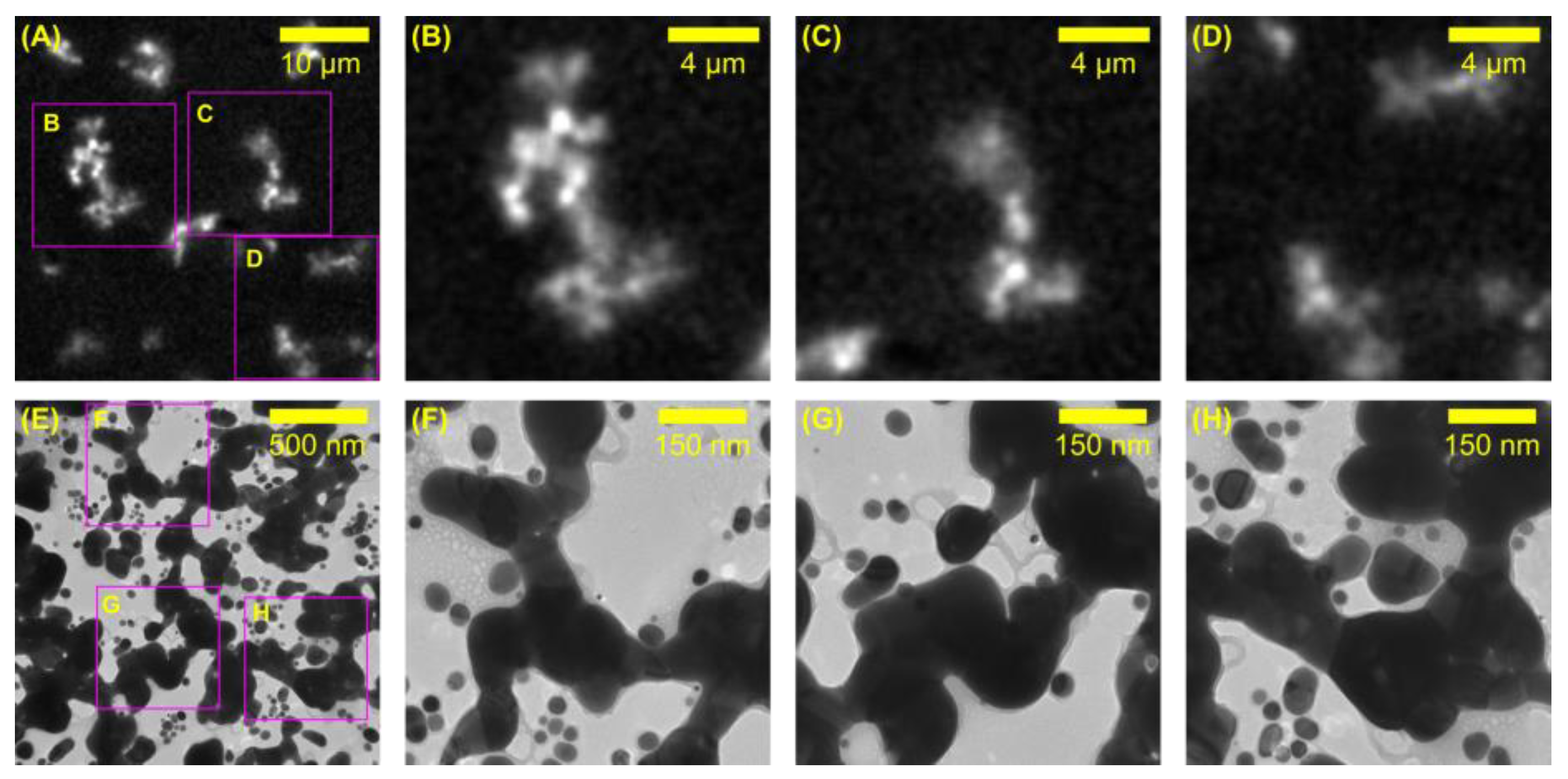
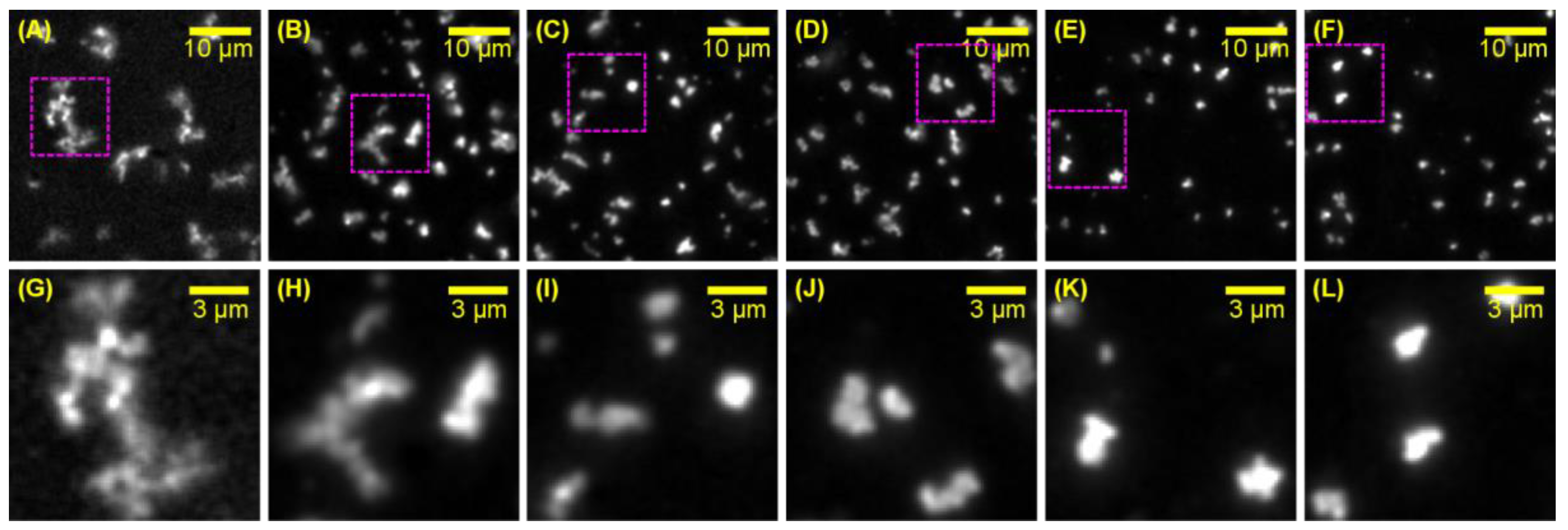
2.2. Fluorescence Microscopy for Imaging of Nanowelded Microstructures of AgNPs
2.3. TEM Imaging of Nanowelded Microstructures
2.4. Automatic Identification of Nanowelded Microstructures of AgNPs
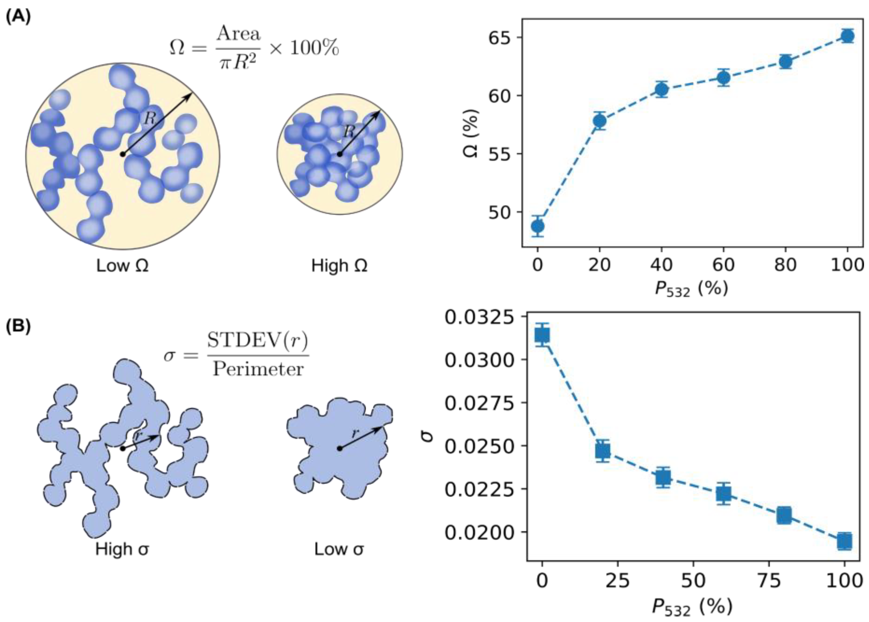
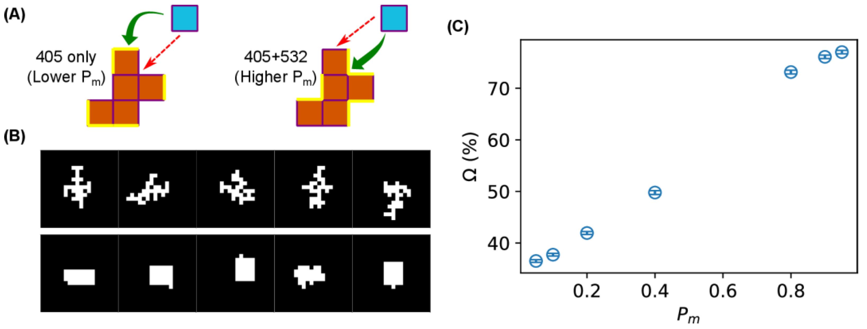
2.5. Shape Analysis of the Nanowelded Microstructures of AgNPs
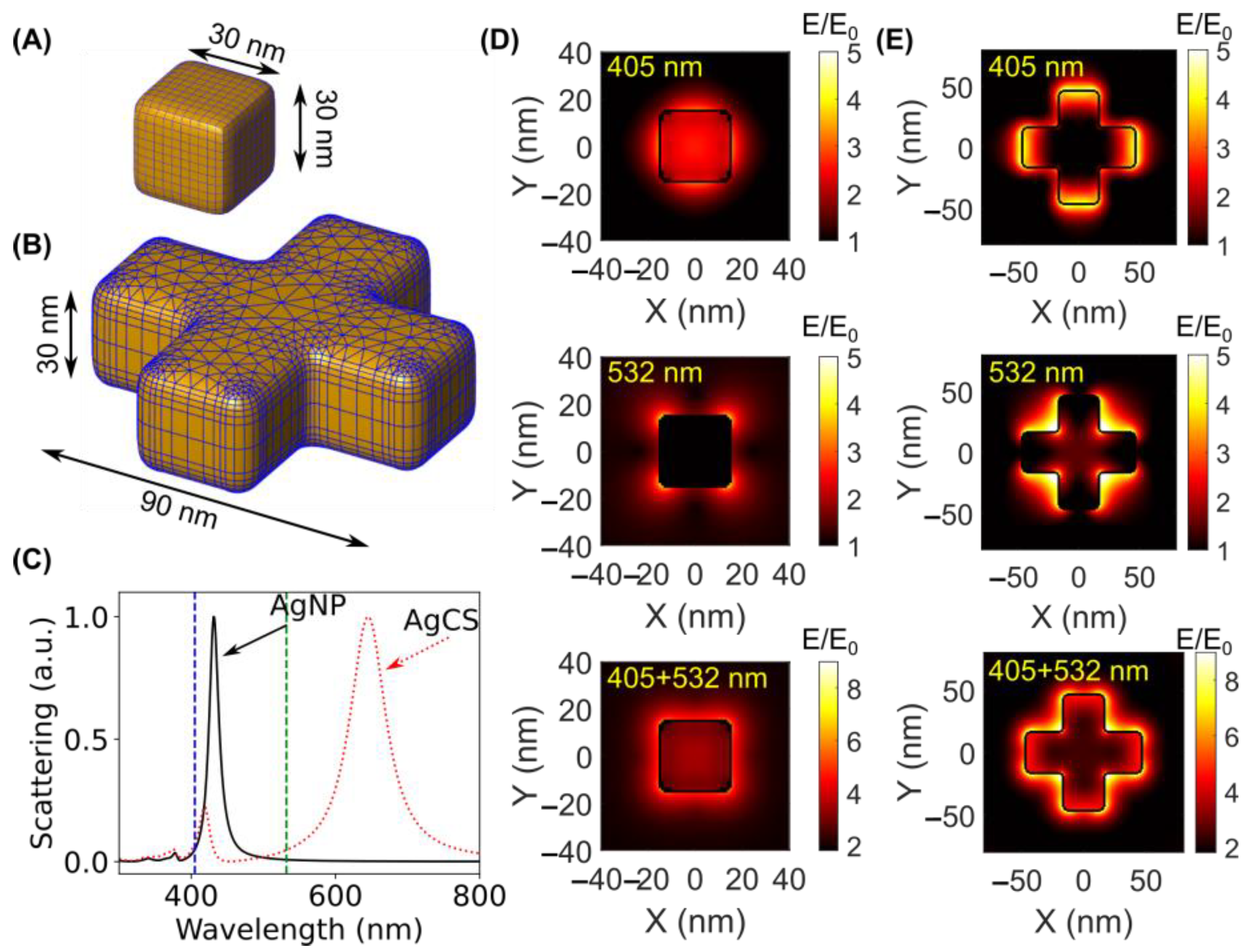
2.6. Calculation of Electric Field Enhancement
2.7. Simulation of Growth of Microstructures
3. Results and Discussion
4. Conclusions
Supplementary Materials
Author Contributions
Funding
Data Availability Statement
Acknowledgments
Conflicts of Interest
References
- Ferrera, M.; Della Valle, G.; Sygletou, M.; Magnozzi, M.; Catone, D.; O’Keeffe, P.; Paladini, A.; Toschi, F.; Mattera, L.; Canepa, M.; et al. Thermometric Calibration of the Ultrafast Relaxation Dynamics in Plasmonic Au Nanoparticles. ACS Photonics 2020, 7, 959–966. [Google Scholar] [CrossRef]
- Govorov, A.O.; Richardson, H.H. Generating Heat with Metal Nanoparticles. Nano Today 2007, 2, 30–38. [Google Scholar] [CrossRef]
- Li, H.; He, Y.; Wang, C.; Wang, X.; Hu, Y. Tunable Thermal and Electricity Generation Enabled by Spectrally Selective Absorption Nanoparticles for Photovoltaic/Thermal Applications. Appl. Energy 2019, 236, 117–126. [Google Scholar] [CrossRef]
- Naito, M.; Yokoyama, T.; Hosokawa, K.; Nogi, K. Nanoparticle Technology Handbook; Elsevier: Amsterdam, The Netherlands, 2018; ISBN 978-0-444-64111-3. [Google Scholar]
- Praetorius, A.; Scheringer, M.; Hungerbühler, K. Development of Environmental Fate Models for Engineered Nanoparticles—A Case Study of TiO2 Nanoparticles in the Rhine River. Environ. Sci. Technol. 2012, 46, 6705–6713. [Google Scholar] [CrossRef]
- Sarina, S.; Waclawik, E.R.; Zhu, H. Photocatalysis on Supported Gold and Silver Nanoparticles under Ultraviolet and Visible Light Irradiation. Green Chem. 2013, 15, 1814–1833. [Google Scholar] [CrossRef]
- Xin, S.; Shen, J.; Liu, G.; Chen, Q.; Xiao, Z.; Zhang, G.; Xin, Y. Electricity Generation and Microbial Community of Single-Chamber Microbial Fuel Cells in Response to Cu2O Nanoparticles/Reduced Graphene Oxide as Cathode Catalyst. Chem. Eng. J. 2020, 380, 122446. [Google Scholar] [CrossRef]
- Fukuta, M.; Ono, A.; Nawa, Y.; Inami, W.; Shen, L.; Kawata, Y.; Terekawa, S. Cell Structure Imaging with Bright and Homogeneous Nanometric Light Source. J. Biophotonics 2017, 10, 503–510. [Google Scholar] [CrossRef]
- Galanzha, E.I.; Nedosekin, D.A.; Sarimollaoglu, M.; Orza, A.I.; Biris, A.S.; Verkhusha, V.V.; Zharov, V.P. Photoacoustic and Photothermal Cytometry Using Photoswitchable Proteins and Nanoparticles with Ultrasharp Resonances. J. Biophotonics 2015, 8, 81–93. [Google Scholar] [CrossRef]
- Kim, S.J.; Jang, D.-J. Laser-Induced Nanowelding of Gold Nanoparticles. Appl. Phys. Lett. 2005, 86, 33112. [Google Scholar] [CrossRef]
- Zhao, Z.-J.; Shin, S.-H.; Choi, D.-G.; Park, S.-H.; Jeong, J.-H. Shape-Controlled 3D Periodic Metal Nanostructures Fabricated via Nanowelding. Small 2018, 14, 1703102. [Google Scholar] [CrossRef]
- Rogers, A.; Niyonshuti, I.I.; Cai, A.; Wang, F.; Benamara, M.; Chen, J.; Wang, Y. Real-Time Imaging of Laser-Induced Nanowelding of Silver Nanoparticles in Solution. J. Phys. Chem. C 2021, 125, 10422–10430. [Google Scholar] [CrossRef]
- Hu, A.; Zhou, Y.; Duley, W. Femtosecond Laser-Induced Nanowelding: Fundamentals and Applications. Open Surf. Sci. J. 2011, 3, 42–49. [Google Scholar] [CrossRef]
- Li, M.; Xie, X.; Xu, Y.; Liu, J.; Fu, Y.; Han, M.; Li, X.; Duan, X.; Min, C.; Hu, J. External Field-Strengthened Ostwald Nanowelding. Nano Res. 2022, 15, 4525–4535. [Google Scholar] [CrossRef]
- Garnett, E.C.; Cai, W.; Cha, J.J.; Mahmood, F.; Connor, S.T.; Greyson Christoforo, M.; Cui, Y.; McGehee, M.D.; Brongersma, M.L. Self-Limited Plasmonic Welding of Silver Nanowire Junctions. Nat. Mater. 2012, 11, 241–249. [Google Scholar] [CrossRef] [PubMed]
- González-Rubio, G.; Guerrero-Martínez, A.; Liz-Marzán, L.M. Reshaping, Fragmentation, and Assembly of Gold Nanoparticles Assisted by Pulse Lasers. Acc. Chem. Res. 2016, 49, 678–686. [Google Scholar] [CrossRef] [PubMed]
- Cha, S.-H.; Park, Y.; Han, J.W.; Kim, K.; Kim, H.-S.; Jang, H.-L.; Cho, S. Cold Welding of Gold Nanoparticles on Mica Substrate: Self-Adjustment and Enhanced Diffusion. Sci. Rep. 2016, 6, 32951. [Google Scholar] [CrossRef]
- Cha, S.-H.; Kang, S.-H.; Lee, Y.J.; Kim, J.-H.; Ahn, E.-Y.; Park, Y.; Cho, S. Fabrication of Nanoribbons by Dielectrophoresis Assisted Cold Welding of Gold Nanoparticles on Mica Substrate. Sci. Rep. 2019, 9, 3629. [Google Scholar] [CrossRef]
- Cui, J.; Theogene, B.; Wang, X.; Mei, X.; Wang, W.; Wang, K. Molecular Dynamics Study of Nanojoining between Axially Positioned Ag Nanowires. Appl. Surf. Sci. 2016, 378, 57–62. [Google Scholar] [CrossRef]
- Lagrange, M.; Langley, D.P.; Giusti, G.; Jiménez, C.; Bréchet, Y.; Bellet, D. Optimization of Silver Nanowire-Based Transparent Electrodes: Effects of Density, Size and Thermal Annealing. Nanoscale 2015, 7, 17410–17423. [Google Scholar] [CrossRef]
- Song, T.-B.; Chen, Y.; Chung, C.-H.; Yang, Y.M.; Bob, B.; Duan, H.-S.; Li, G.; Tu, K.-N.; Huang, Y.; Yang, Y. Nanoscale Joule Heating and Electromigration Enhanced Ripening of Silver Nanowire Contacts. ACS Nano 2014, 8, 2804–2811. [Google Scholar] [CrossRef]
- Tseng, J.-Y.; Lee, L.; Huang, Y.-C.; Chang, J.-H.; Su, T.-Y.; Shih, Y.-C.; Lin, H.-W.; Chueh, Y.-L. Pressure Welding of Silver Nanowires Networks at Room Temperature as Transparent Electrodes for Efficient Organic Light-Emitting Diodes. Small 2018, 14, 1800541. [Google Scholar] [CrossRef] [PubMed]
- Kim, J.; Nam, Y.S.; Song, M.H.; Park, H.W. Large Pulsed Electron Beam Welded Percolation Networks of Silver Nanowires for Transparent and Flexible Electrodes. ACS Appl. Mater. Interfaces 2016, 8, 20938–20945. [Google Scholar] [CrossRef] [PubMed]
- Jin, R.; Cao, Y.; Mirkin, C.A.; Kelly, K.L.; Schatz, G.C.; Zheng, J.G. Photoinduced Conversion of Silver Nanospheres to Nanoprisms. Science 2001, 294, 1901–1903. [Google Scholar] [CrossRef] [PubMed]
- Jin, R.; Charles Cao, Y.; Hao, E.; Métraux, G.S.; Schatz, G.C.; Mirkin, C.A. Controlling Anisotropic Nanoparticle Growth through Plasmon Excitation. Nature 2003, 425, 487–490. [Google Scholar] [CrossRef] [PubMed]
- Catone, D.; Ciavardini, A.; Di Mario, L.; Paladini, A.; Toschi, F.; Cartoni, A.; Fratoddi, I.; Venditti, I.; Alabastri, A.; Proietti Zaccaria, R.; et al. Plasmon Controlled Shaping of Metal Nanoparticle Aggregates by Femtosecond Laser-Induced Melting. J. Phys. Chem. Lett. 2018, 9, 5002–5008. [Google Scholar] [CrossRef] [PubMed]
- Herrmann, L.O.; Valev, V.K.; Tserkezis, C.; Barnard, J.S.; Kasera, S.; Scherman, O.A.; Aizpurua, J.; Baumberg, J.J. Threading Plasmonic Nanoparticle Strings with Light. Nat. Commun. 2014, 5, 4568. [Google Scholar] [CrossRef]
- Zhang, D.; Gökce, B.; Barcikowski, S. Laser Synthesis and Processing of Colloids: Fundamentals and Applications. Chem. Rev. 2017, 117, 3990–4103. [Google Scholar] [CrossRef]
- Rycenga, M.; Cobley, C.M.; Zeng, J.; Li, W.; Moran, C.H.; Zhang, Q.; Qin, D.; Xia, Y. Controlling the Synthesis and Assembly of Silver Nanostructures for Plasmonic Applications. Chem. Rev. 2011, 111, 3669–3712. [Google Scholar] [CrossRef]
- Chao, C.-T.C.; Kooh, M.R.R.; Lim, C.M.; Thotagamuge, R.; Mahadi, A.H.; Chau, Y.-F.C. Visible-Range Multiple-Channel Metal-Shell Rod-Shaped Narrowband Plasmonic Metamaterial Absorber for Refractive Index and Temperature Sensing. Micromachines 2023, 14, 340. [Google Scholar] [CrossRef]
- Chao, C.-T.C.; Kooh, M.R.R.; Chau, Y.-F.C.; Thotagamuge, R. Susceptible Plasmonic Photonic Crystal Fiber Sensor with Elliptical Air Holes and External-Flat Gold-Coated Surface. Photonics 2022, 9, 916. [Google Scholar] [CrossRef]
- Ru, E.C.L.; Etchegoin, P.G. Principles of Surface-Enhanced Raman Spectroscopy: And Related Plasmonic Effects; Elsevier Science & Technology Books: Amsterdam, The Netherlands, 2009; ISBN 978-0-444-52779-0. [Google Scholar]
- Kuppe, C.; Rusimova, K.R.; Ohnoutek, L.; Slavov, D.; Valev, V.K. “Hot” in Plasmonics: Temperature-Related Concepts and Applications of Metal Nanostructures. Adv. Opt. Mater. 2020, 8, 1901166. [Google Scholar] [CrossRef]
- Ghosh, S.K.; Pal, T. Interparticle Coupling Effect on the Surface Plasmon Resonance of Gold Nanoparticles: From Theory to Applications. Chem. Rev. 2007, 107, 4797–4862. [Google Scholar] [CrossRef] [PubMed]
- Marchuk, K.; Willets, K.A. Localized Surface Plasmons and Hot Electrons. Chem. Phys. 2014, 445, 95–104. [Google Scholar] [CrossRef]
- Petryayeva, E.; Krull, U.J. Localized Surface Plasmon Resonance: Nanostructures, Bioassays and Biosensing—A Review. Anal. Chim. Acta 2011, 706, 8–24. [Google Scholar] [CrossRef]
- Zhang, Q.; Li, W.; Moran, C.; Zeng, J.; Chen, J.; Wen, L.-P.; Xia, Y. Seed-Mediated Synthesis of Ag Nanocubes with Controllable Edge Lengths in the Range of 30-200 Nm and Comparison of Their Optical Properties. J. Am. Chem. Soc. 2010, 132, 11372–11378. [Google Scholar] [CrossRef]
- Haque, M.A.; Imamura, R.; Brown, G.A.; Krishnamurthi, V.R.; Niyonshuti, I.I.; Marcelle, T.; Mathurin, L.E.; Chen, J.; Wang, Y. An Experiment-Based Model Quantifying Antimicrobial Activity of Silver Nanoparticles onEscherichia Coli. RSC Adv. 2017, 7, 56173–56182. [Google Scholar] [CrossRef]
- Alqahtany, M.; Khadka, P.; Niyonshuti, I.; Krishnamurthi, V.R.; Sadoon, A.A.; Challapalli, S.D.; Chen, J.; Wang, Y. Nanoscale Reorganizations of Histone-like Nucleoid Structuring Proteins in Escherichia Coli Are Caused by Silver Nanoparticles. Nanotechnology 2019, 30, 385101. [Google Scholar] [CrossRef]
- Niyonshuti, I.I.; Krishnamurthi, V.R.; Okyere, D.; Song, L.; Benamara, M.; Tong, X.; Wang, Y.; Chen, J. Polydopamine Surface Coating Synergizes the Antimicrobial Activity of Silver Nanoparticles. ACS Appl. Mater. Interfaces 2020, 12, 40067–40077. [Google Scholar] [CrossRef]
- Laramy, C.R.; Brown, K.A.; O’Brien, M.N.; Mirkin, C.A. High-Throughput, Algorithmic Determination of Nanoparticle Structure from Electron Microscopy Images. ACS Nano 2015, 9, 12488–12495. [Google Scholar] [CrossRef]
- Selvin, P.R.; Ha, T. Single Molecule Techniques: A Laboratory Manual, 1st ed.; Cold Spring Harbor Laboratory Press: Cold Spring Harbor, NY, USA, 2007; ISBN 0-87969-775-X. [Google Scholar]
- Wang, Y.; Cai, E.; Sheung, J.; Lee, S.H.; Teng, K.W.; Selvin, P.R. Fluorescence Imaging with One-Nanometer Accuracy (FIONA). J. Vis. Exp. 2014, 91, 51774. [Google Scholar] [CrossRef]
- Ashenfelter, B.A.; Desireddy, A.; Yau, S.H.; Goodson, T.; Bigioni, T.P. Fluorescence from Molecular Silver Nanoparticles. J. Phys. Chem. C 2015, 119, 20728–20734. [Google Scholar] [CrossRef]
- Yeshchenko, O.A.; Dmitruk, I.M.; Alexeenko, A.A.; Losytskyy, M.Y.; Kotko, A.V.; Pinchuk, A.O. Size-Dependent Surface-Plasmon-Enhanced Photoluminescence from Silver Nanoparticles Embedded in Silica. Phys. Rev. B 2009, 79, 235438. [Google Scholar] [CrossRef]
- Edelstein, A.; Amodaj, N.; Hoover, K.; Vale, R.; Stuurman, N. Computer Control of Microscopes Using µManager. Curr Protoc Mol Biol 2010, 92, 14.20.1–14.20.17. [Google Scholar] [CrossRef]
- Edelstein, A.D.; Tsuchida, M.A.; Amodaj, N.; Pinkard, H.; Vale, R.D.; Stuurman, N. Advanced Methods of Microscope Control Using μManager Software. J. Biol. Methods 2014, 1, e10. [Google Scholar] [CrossRef] [PubMed]
- van der Walt, S.; Schönberger, J.L.; Nunez-Iglesias, J.; Boulogne, F.; Warner, J.D.; Yager, N.; Gouillart, E.; Yu, T. Scikit-image contributors Scikit-Image: Image Processing in Python. PeerJ 2014, 2, e453. [Google Scholar] [CrossRef] [PubMed]
- Sternberg. Biomedical Image Processing. Computer 1983, 16, 22–34. [Google Scholar] [CrossRef]
- Kanopoulos, N.; Vasanthavada, N.; Baker, R.L. Design of an Image Edge Detection Filter Using the Sobel Operator. IEEE J. Solid-State Circuits 1988, 23, 358–367. [Google Scholar] [CrossRef]
- Nosal, E. Flood-Fill Algorithms Used for Passive Acoustic Detection and Tracking. In Proceedings of the 2008 New Trends for Environmental Monitoring Using Passive Systems, Hyeres, France, 14–17 October 2008; pp. 1–5. [Google Scholar]
- Kindratenko, V.V. On Using Functions to Describe the Shape. J. Math. Imaging Vis. 2003, 18, 225–245. [Google Scholar] [CrossRef]
- Braden, B. The Surveyor’s Area Formula. Coll. Math. J. 1986, 17, 326–337. [Google Scholar] [CrossRef]
- Wang, Y.; Zocchi, G. Shape of Fair Weather Clouds. Phys. Rev. Lett. 2010, 104, 118502. [Google Scholar] [CrossRef]
- Hohenester, U.; Trügler, A. MNPBEM—A Matlab Toolbox for the Simulation of Plasmonic Nanoparticles. Comput. Phys. Commun. 2012, 183, 370–381. [Google Scholar] [CrossRef]
- Waxenegger, J.; Trügler, A.; Hohenester, U. Plasmonics Simulations with the MNPBEM Toolbox: Consideration of Substrates and Layer Structures. Comput. Phys. Commun. 2015, 193, 138–150. [Google Scholar] [CrossRef]
- Hohenester, U. Simulating Electron Energy Loss Spectroscopy with the MNPBEM Toolbox. Comput. Phys. Commun. 2014, 185, 1177–1187. [Google Scholar] [CrossRef]
- Haiss, W.; Thanh, N.T.K.; Aveyard, J.; Fernig, D.G. Determination of Size and Concentration of Gold Nanoparticles from UV−Vis Spectra. Anal. Chem. 2007, 79, 4215–4221. [Google Scholar] [CrossRef] [PubMed]
- Paramelle, D.; Sadovoy, A.; Gorelik, S.; Free, P.; Hobley, J.; Fernig, D.G. A Rapid Method to Estimate the Concentration of Citrate Capped Silver Nanoparticles from UV-Visible Light Spectra. Analyst 2014, 139, 4855–4861. [Google Scholar] [CrossRef] [PubMed]
- Sørensen, L.K.; Khrennikov, D.E.; Gerasimov, V.S.; Ershov, A.E.; Polyutov, S.P.; Karpov, S.V.; Ågren, H. Nature of the Anomalous Size Dependence of Resonance Red Shifts in Ultrafine Plasmonic Nanoparticles. J. Phys. Chem. C 2022, 126, 16804–16814. [Google Scholar] [CrossRef]
- Draine, B.T.; Flatau, P.J. Discrete-Dipole Approximation for Periodic Targets: Theory and Tests. J. Opt. Soc. Am. A 2008, 25, 2693–2703. [Google Scholar] [CrossRef]
- Draine, B.T.; Flatau, P.J. User Guide for the Discrete Dipole Approximation Code DDSCAT 7.3. arXiv 2013, arXiv:1305.6497. [Google Scholar]
- Agrawal, A.; Cho, S.H.; Zandi, O.; Ghosh, S.; Johns, R.W.; Milliron, D.J. Localized Surface Plasmon Resonance in Semiconductor Nanocrystals. Chem. Rev. 2018, 118, 3121–3207. [Google Scholar] [CrossRef]
- Chao, C.-T.C.; Chau, Y.-F.C.; Chiang, H.-P. Highly Sensitive Metal-Insulator-Metal Plasmonic Refractive Index Sensor with a Centrally Coupled Nanoring Containing Defects. J. Phys. D Appl. Phys. 2021, 54, 115301. [Google Scholar] [CrossRef]
- Amicucci, C.; D’Andrea, C.; de Angelis, M.; Banchelli, M.; Pini, R.; Matteini, P. Cost Effective Silver Nanowire-Decorated Graphene Paper for Drop-On SERS Biodetection. Nanomaterials 2021, 11, 1495. [Google Scholar] [CrossRef] [PubMed]
- Kim, S.; Jin, J.; Kim, Y.-J.; Park, I.-Y.; Kim, Y.; Kim, S.-W. High-Harmonic Generation by Resonant Plasmon Field Enhancement. Nature 2008, 453, 757–760. [Google Scholar] [CrossRef] [PubMed]
- Zhang, A.; Zhang, J.; Fang, Y. Photoluminescence from Colloidal Silver Nanoparticles. J. Lumin. 2008, 128, 1635–1640. [Google Scholar] [CrossRef]
- He, H.; Xie, C.; Ren, J. Nonbleaching Fluorescence of Gold Nanoparticles and Its Applications in Cancer Cell Imaging. Anal. Chem. 2008, 80, 5951–5957. [Google Scholar] [CrossRef] [PubMed]
- Geddes, C.D.; Parfenov, A.; Gryczynski, I.; Lakowicz, J.R. Luminescent Blinking of Gold Nanoparticles. Chem. Phys. Lett. 2003, 380, 269–272. [Google Scholar] [CrossRef]
- Geddes, C.D.; Parfenov, A.; Lakowicz, J.R. Luminescent Blinking from Noble-Metal Nanostructures: New Probes for Localization and Imaging. J. Fluoresc. 2003, 13, 297–299. [Google Scholar] [CrossRef]
- Gaiduk, A.; Ruijgrok, P.V.; Yorulmaz, M.; Orrit, M. Making Gold Nanoparticles Fluorescent for Simultaneous Absorption and Fluorescence Detection on the Single Particle Level. Phys. Chem. Chem. Phys. 2010, 13, 149–153. [Google Scholar] [CrossRef]
- Wolfbeis, O.S. An Overview of Nanoparticles Commonly Used in Fluorescent Bioimaging. Chem. Soc. Rev. 2015, 44, 4743–4768. [Google Scholar] [CrossRef]
- Qing, Z.; He, X.; Qing, T.; Wang, K.; Shi, H.; He, D.; Zou, Z.; Yan, L.; Xu, F.; Ye, X.; et al. Poly(Thymine)-Templated Fluorescent Copper Nanoparticles for Ultrasensitive Label-Free Nuclease Assay and Its Inhibitors Screening. Anal. Chem. 2013, 85, 12138–12143. [Google Scholar] [CrossRef]
- Verbruggen, S.W.; Keulemans, M.; Martens, J.A.; Lenaerts, S. Predicting the Surface Plasmon Resonance Wavelength of Gold–Silver Alloy Nanoparticles. J. Phys. Chem. C 2013, 117, 19142–19145. [Google Scholar] [CrossRef]
- Kelly, K.L.; Coronado, E.; Zhao, L.L.; Schatz, G.C. The Optical Properties of Metal Nanoparticles: The Influence of Size, Shape, and Dielectric Environment. J. Phys. Chem. B 2003, 107, 668–677. [Google Scholar] [CrossRef]
- Ha, J.; Lee, B.J.; Hwang, D.J.; Kim, D. Femtosecond Laser Nanowelding of Silver Nanowires for Transparent Conductive Electrodes. RSC Adv. 2016, 6, 86232–86239. [Google Scholar] [CrossRef]
- Xu, F.; Xu, W.; Mao, B.; Shen, W.; Yu, Y.; Tan, R.; Song, W. Preparation and Cold Welding of Silver Nanowire Based Transparent Electrodes with Optical Transmittances > 90% and Sheet Resistances < 10 Ohm/Sq. J. Colloid Interface Sci. 2018, 512, 208–218. [Google Scholar] [CrossRef] [PubMed]
- Shou, W.; Mahajan, B.K.; Ludwig, B.; Yu, X.; Staggs, J.; Huang, X.; Pan, H. Low-Cost Manufacturing of Bioresorbable Conductors by Evaporation–Condensation-Mediated Laser Printing and Sintering of Zn Nanoparticles. Adv. Mater. 2017, 29, 1700172. [Google Scholar] [CrossRef]
- Shou, W.; Pan, H. Direct Printing of Microstructures by Femtosecond Laser Excitation of Nanocrystals in Solution. Appl. Phys. Lett. 2016, 108, 214101. [Google Scholar] [CrossRef]
- Podder, C.; Gong, X.; Yu, X.; Shou, W.; Pan, H. Submicron Metal 3D Printing by Ultrafast Laser Heating and Induced Ligand Transformation of Nanocrystals. ACS Appl. Mater. Interfaces 2021, 13, 42154–42163. [Google Scholar] [CrossRef]


Disclaimer/Publisher’s Note: The statements, opinions and data contained in all publications are solely those of the individual author(s) and contributor(s) and not of MDPI and/or the editor(s). MDPI and/or the editor(s) disclaim responsibility for any injury to people or property resulting from any ideas, methods, instructions or products referred to in the content. |
© 2023 by the authors. Licensee MDPI, Basel, Switzerland. This article is an open access article distributed under the terms and conditions of the Creative Commons Attribution (CC BY) license (https://creativecommons.org/licenses/by/4.0/).
Share and Cite
Rogers, A.; Niyonshuti, I.I.; Ou, J.; Shrestha, D.; Okyere, D.; Chen, J.; Wang, Y. The Shape Modulation of Laser-Induced Nanowelded Microstructures Using Two Colors. Colloids Interfaces 2023, 7, 67. https://doi.org/10.3390/colloids7040067
Rogers A, Niyonshuti II, Ou J, Shrestha D, Okyere D, Chen J, Wang Y. The Shape Modulation of Laser-Induced Nanowelded Microstructures Using Two Colors. Colloids and Interfaces. 2023; 7(4):67. https://doi.org/10.3390/colloids7040067
Chicago/Turabian StyleRogers, Ariel, Isabelle I. Niyonshuti, Jun Ou, Diksha Shrestha, Deborah Okyere, Jingyi Chen, and Yong Wang. 2023. "The Shape Modulation of Laser-Induced Nanowelded Microstructures Using Two Colors" Colloids and Interfaces 7, no. 4: 67. https://doi.org/10.3390/colloids7040067
APA StyleRogers, A., Niyonshuti, I. I., Ou, J., Shrestha, D., Okyere, D., Chen, J., & Wang, Y. (2023). The Shape Modulation of Laser-Induced Nanowelded Microstructures Using Two Colors. Colloids and Interfaces, 7(4), 67. https://doi.org/10.3390/colloids7040067