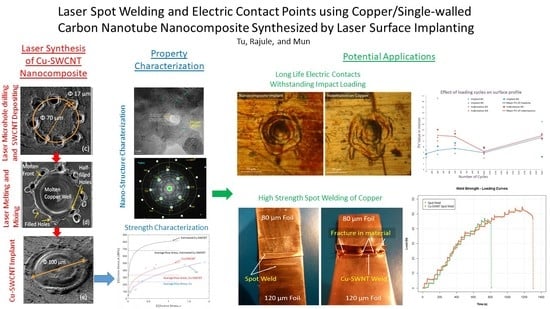
Article

Laser Spot Welding and Electric Contact Points Using Copper/Single-Walled Carbon Nanotube Nanocomposite Synthesized by Laser Surface Implanting

1
Department of Mechanical and Aerospace Engineering, North Carolina State University, Raleigh, NC 27695-8501, USA
2
Independent Consultant, Bengaluru 560002, Karnataka, India
3
Division of Mechanical Design Engineering, Jeonbuk National University, 664-14, Jeonju 561-756, Korea
*
Author to whom correspondence should be addressed.
J. Compos. Sci. 2021, 5(3), 87; https://doi.org/10.3390/jcs5030087
Submission received: 1 March 2021 / Revised: 12 March 2021 / Accepted: 16 March 2021 / Published: 22 March 2021
(This article belongs to the Special Issue Laser Fabrication of Composites)

Abstract

:
In our previous studies, we have developed a wet process, denoted as laser surface implanting (LSI), to synthesize a copper/single-walled carbon nanotube (Cu–SWCNT) metal nanocomposite. The nanostructure of this Cu–SWCNT composite was shown to contain discernable SWCNT clusters in nanosizes inside the copper matrix. Its hardness could achieve up to three times that of pure copper, verified by micro-hardness and nano-hardness tests. A focus ion beam bombardment test and a plane strain compression test show 2.5 times toughness improvement for the Cu-SWCNT composite. Based on these strength improvements, two potential applications for the Cu-SWCNT nanocomposite are proposed and their feasibilities are verified using specially design test rigs. The first application is related to creating long lasting electric contacts. The result shows that the Cu-SWCNT nanocomposite is highly wear-resistant. The contact area of the simulated electric contacts increases after repeated impact loading, which potentially could lower the contact resistance. The second application is to use the Cu-SWCNT implants as high strength spot weld for joining copper foils. A smaller weld with a higher strength reduces the power requirement of the laser and, consequently, the thermal distortion for higher-dimensional precision. The specially designed test rig for the weld strength characterization is a new contribution, providing a new testing capability for small and non-homogeneous samples not suitable for a standard tensile test machine.

Graphical Abstract

1. Introduction

Carbon nanotubes (CNTs), due to their exceptional structural properties, are ideal reinforcing elements for high strength composite. CNT-reinforced composite research first focused on polymer composites, and, subsequently, metal composites [1,2].
Copper is one of the most important industrial materials due to its excellent thermal and electric conductivities. However, copper is a soft material with poor wear resistance. Although copper alloys, such as brass, offer higher strength over pure copper, they suffer substantial reductions in both thermal and electric conductivities. If copper could be strengthened without loss of these two properties, it would become an ideal material for many critical applications. In order to retain both thermal and electric properties of copper, the reinforcement element likely needs to have equal or superior thermal and electric properties. One such reinforcement candidate is carbon nanotubes (CNTs).
However, the synthesis of Cu-CNT composites is, in general, more difficult than Al-CNT composites because copper and carbon do not form intermetallic compounds, as in the case of aluminum and carbon to form aluminum carbide. In addition, copper and carbon are not soluble. As a result, most Cu-CNT synthesis processes, reported in the literature, are based on powder metallurgy, which is denoted as the dry process in this paper. A detailed review of powder metallurgy-based processes and the properties of thus-formed CNT-reinforced composites can be found in [3,4]. Typically, ball milling is used to mix copper powder and carbon nanotubes, followed by sintering to form the Cu-CNT composite in the dry process [5,6]. The strength improvements using the dry process typically are between 40 and 200% that of pure copper, with 15–20% CNT volume fraction [7,8]. The high CNT volume fraction makes the dry process not cost effective because of the high cost of CNTs, particularly if the improvement is limited.
The limited strength improvement of the Cu-CNT composite synthesized by the dry process is mainly due to the large clusters of CNT within the copper matrix. CNTs’ tremendous surface area results in large van der Waals forces; as a result, it is very difficult to break up CNTs into sub-micron clusters despite long hours of mixing by ball-end mills.
One recent synthesis of Cu-CNT composite via powder metallurgy is to allow CNT to form graphene-like structure to wrap around Cu particles [9]. The reported improvement of the ultimate strength improvement is about 50% with a volume fraction of 40 to 60%.
In addition to the powder metallurgy, there are other dry processes such as electrode-deposition [10] and spark plasma sintering [11]. The strength improvements are limited similar to those by the powder metallurgy using similarly high-volume fractions of CNTs.
The thermal property of Cu-Diamond composite using the dry process was investigated in [12]. The thermal conductivity improves from 364 W/mK (pure copper) to 437 W/mK for the Cu-Diamond composite with a fraction volume of diamond of 30%.
The electricity property of Cu-CNT composite using the dry process was investigated in [13]. The electric conductivity deteriorates from 60 MS/m (pure copper) to 50 MS/m for Cu-MWCNT composite at 0.1% volume fraction, and to less than 30 MS/m at 2% volume fraction. Correspondingly, the Brinell hardness improves from 55 HBN (pure copper) to 84 HBN for Cu-CNT at 0.1% volume fraction. At higher volume fractions, the hardness does not improve, but deteriorates slightly.
In the next few sections, a comprehensive and yet concise review is presented for a “Wet” Cu-CNT synthesis process and the properties of resulting Cu-CNT composite. The review provides the required properties and justifications for the proposed new applications in this paper.

1.1. Wet Synthesis of Cu-SWCNT Nanocomposite and Resulting Nanostructures

A wet process, denoted as Laser Surface Implanting (LSI), was reported in [3,4] for the synthesis of a copper–single-walled carbon nanotube (Cu-SWCNT) nanocomposites. This process disperses single-walled carbon nanotube (SWCNTs) into molten copper, followed by rapid and non-equilibrium solidification to lock SWCNTs in positions, without giving sufficient time for them to agglomerate into large clusters. Rapid and non-equilibrium solidification is achieved when the heat of the molten copper is rapidly conducted away into the copper substrate due to copper’s excellent heat conductivity.
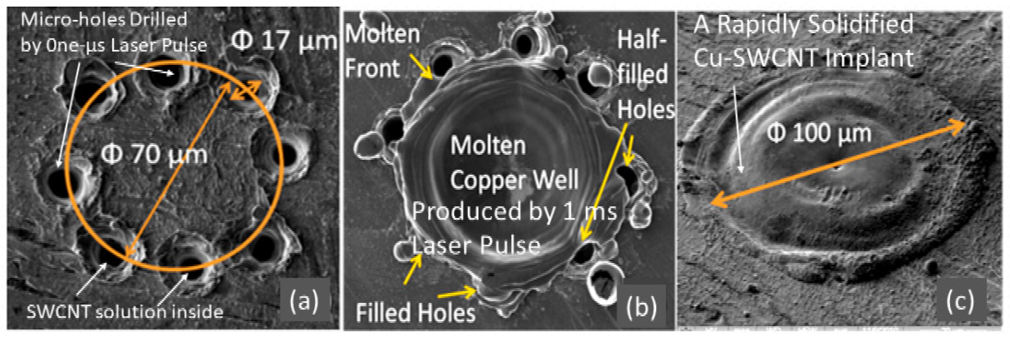
As shown in Figure 1, this novel synthesis process includes: Step (1): A 1 µs laser pulse, produced by a 300 W single-mode fiber laser, is focused to a 10 µm spot size to drill a number of microholes (17 µm in diameter and depth) arranged around a circle of 70 µm diameter (Figure 1a). Step (2): The microholes are filled with SWCNTs suspended in solution. Step (3): A laser pulse of 1 ms, from the same laser with the same spot size of 10 µm, is applied at the center of the above microhole circle. The longer laser pulse creates a well of molten copper. The molten copper advances radially outward to engulf the micro-holes filled with pre-deposited SWCNTs (Figure 1b). After the laser pulse ends, a Cu-SWCNT implant is formed (Figure 1c) due to rapid and non-equilibrium solidification which locks dispersed SWCNTs in place without agglomerating into large clusters, unlike the large clusters seen in the dry process (Figure 2) [14].
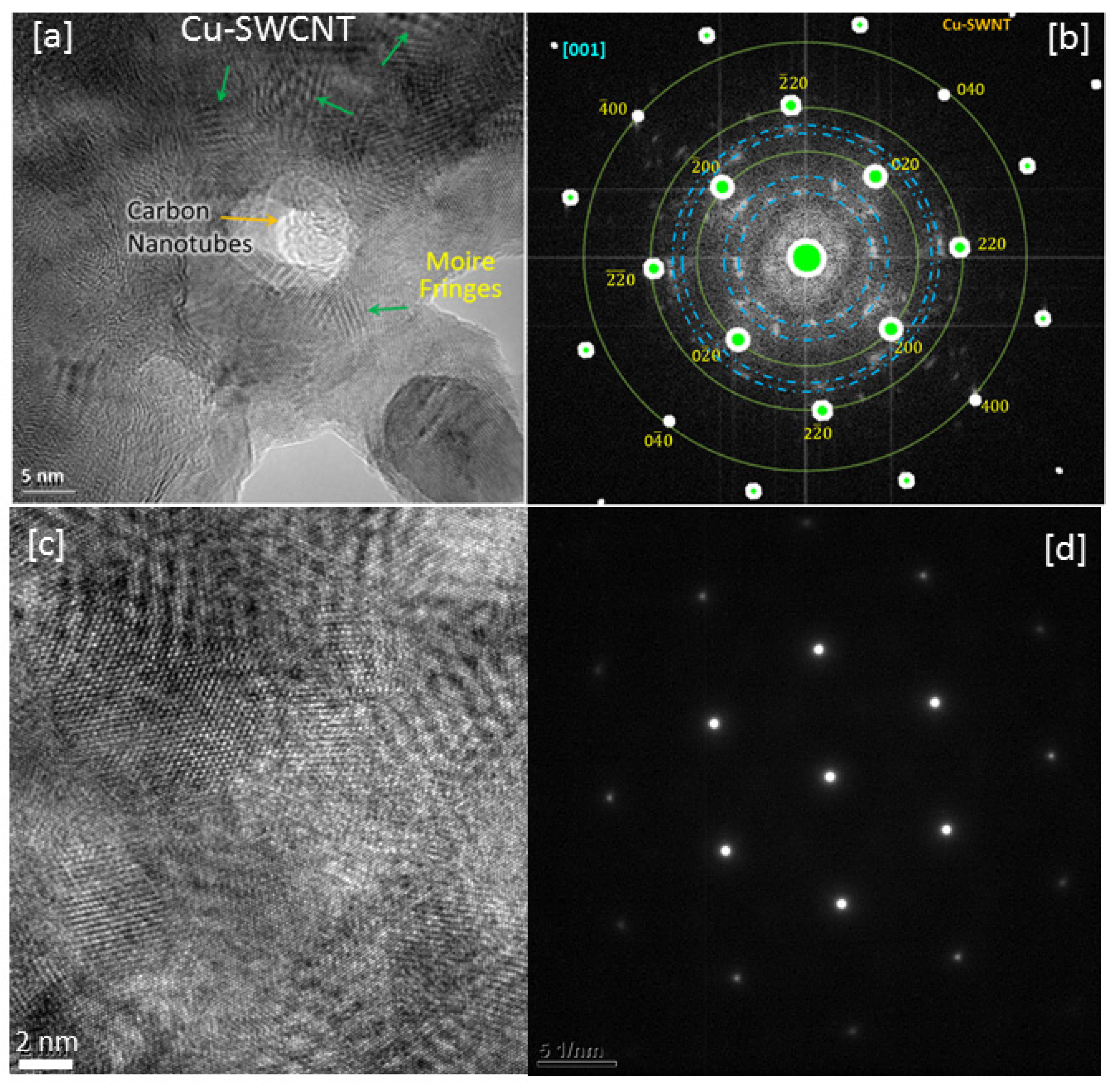
The nanostructure of the Cu–SWCNT composite is confirmed independently by energy dispersive X-ray spectroscopy mapping, spectroscopy measurements, and TEM images (Figure 2a) [14]. Nanosized SWCNT clusters inside the copper matrix are observed. The corresponding refraction index patterns of the TEM image of Figure 2a is shown in Figure 2b. The bright dots in Figure 2b are related to copper’s atomic lattice structure, while the clouds are related to the SWCNT clusters within the copper matrix [14].
Many detailed TEM images of the Cu-SWCNT with their corresponding refraction index patterns were presented in [14]. However, TEM images with discernable nanosized SWCNT clusters are rare, the analysis of indirect TEM image patterns, such as moiré fringes, to infer the existence of SWCNT clusters within the copper matrix was presented in [15]. Figure 2c is the TEM image of a pure copper sample. Its corresponding refraction index pattern is shown in Figure 2d. No bright clouds are found in Figure 2d for pure copper, drastically different from Figure 2b.
The nanostructure of the Cu-SWCNT composite synthesized by the wet process is favorable to achieve higher strength improvement due to the nanosized clusters. However, due to the small size and inhomogeneous structure of the Cu-SWCNT composite, standard tensile testing machines (universal testers) cannot be used. Several unique tests are reviewed in the several sections to verify the mechanical properties of the composite regarding its hardness, toughness, and stress–strain behavior. These properties are important for the proposed applications.

1.2. Hardness Tests for Cu-SWCNT

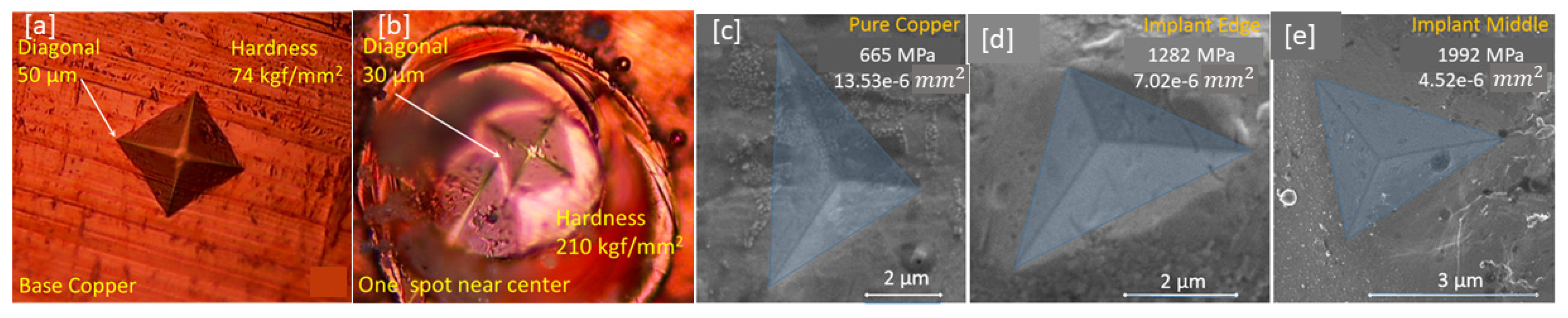
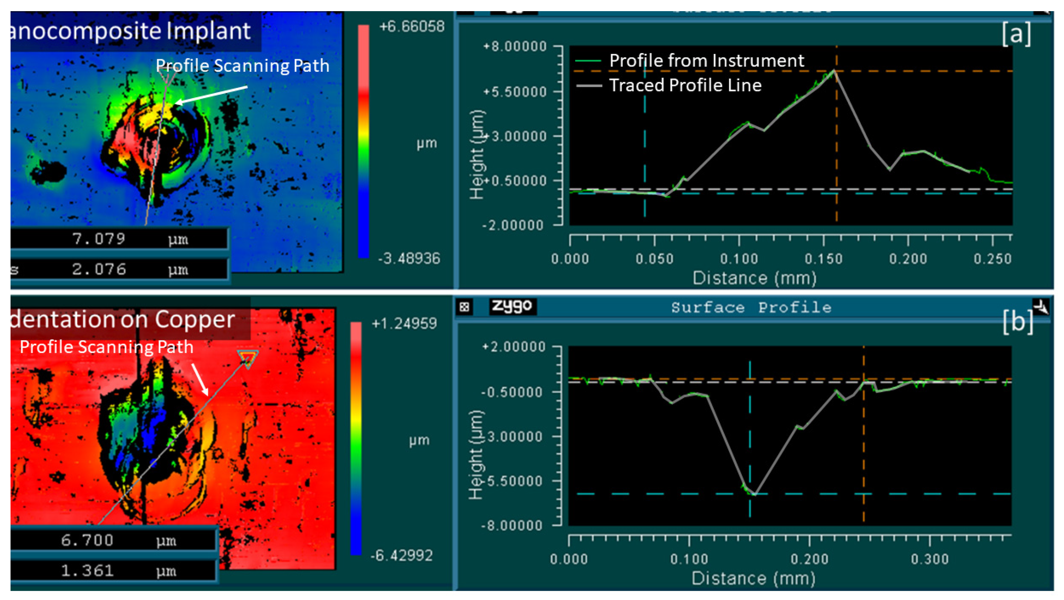
Micro- and nano-hardness tests results for the Cu-SWCNT nanocomposite were presented in Figure 3a,b [4].
A Tukon micro-hardness tester with a Vickers diamond square-based pyramid indenter was used to measure the hardness of Cu-SWCNT nanocomposite at 100 gmf load. The micro-hardness for pure copper was found to be 74 kgf/mm2 (HV 74) (Figure 3a). A micro-hardness of 210 kgf/mm2 (HV 210) was found in some Cu-SWCNT samples (Figure 3b). This hardness is 285% that of pure copper, harder than the hardest brass (cold-rolled, HV 180).
Nano-indentation tests were performed using Hysitron Ubi-1 Triboindenter (Bruker Nano Surface Offices, Billerica, MA, USA) with the Berkovich indenter. At the edge of the implant, the hardness was found to be 1282 MPa (Figure 3d), or 197% that of pure copper at 665 MPa (Figure 3c), while the implant surface in the middle region could have a hardness of 1992 MPa (Figure 3e), which is about 306% that of pure copper. While the center nano-hardness is consistent with the micro-hardness test results, the perimeter hardness is lower. The hardness of the Cu-SWCNT nanocomposite is not uniform based on Figure 3. Please refer to the work in [16] for details of the nano-hardness test conditions and results.

1.3. Toughness and Stress–Strain Tests

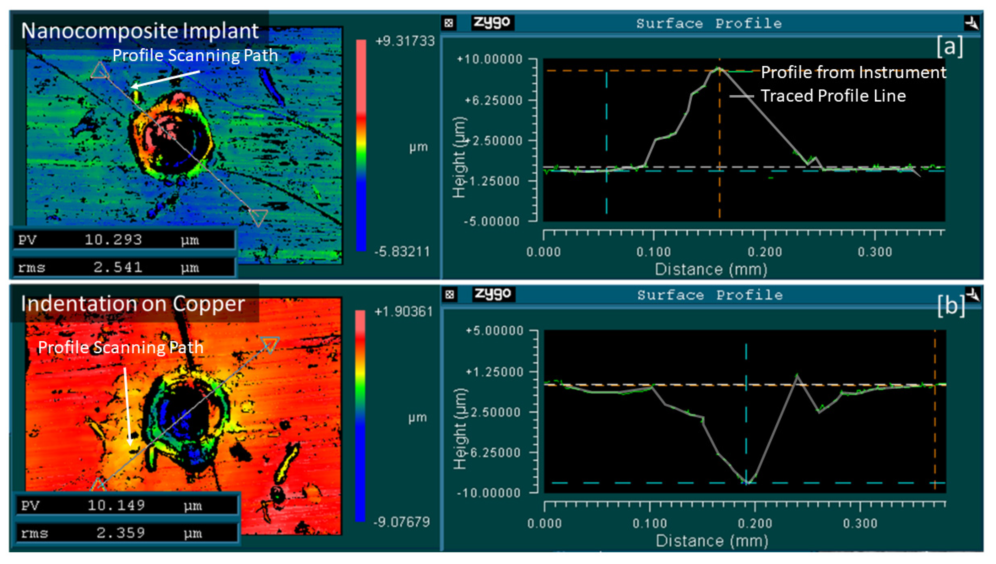
A new toughness characterization study of the Cu-SWCNT nanocomposite implant was carried out using a focused ion beam (FIB) machine (FEI Quanta 3D FEG, ThermoFisher Scientific, Hillsboro, OR, USA) [16]. FIB is an effective tool to process samples for TEM measurements. FIB contains energized ions, which kinetic energy can be programmed to precise values. When an energized ion hits a sample, a small amount of the material is removed because the removed material absorbs the ion energy which exceeds the toughness of the material. Note that the definition of toughness is the energy absorbed by a unit mass of material until fracture. Toughness is corresponding to the area under a stress–strain curve from a standard tensile test. Therefore, if the kinetic energy of the bombardment ion is kept constant and the material is bombarded for a fixed amount of time, then the amounts of material removed will be proportional to the toughness of the material. Therefore, this new toughness characterization method is denoted as the toughness test via ion bombardment [16].
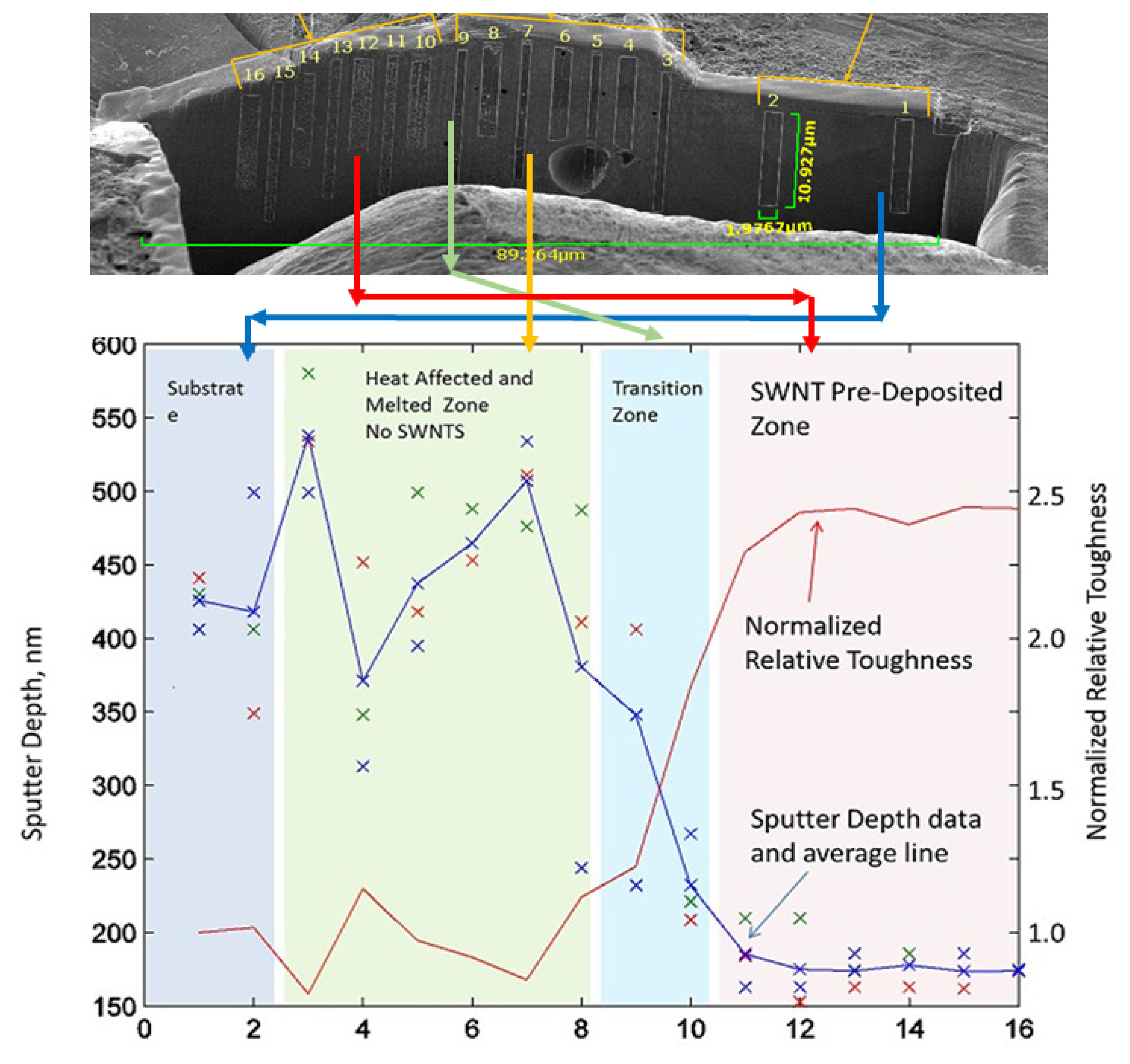
Before performing the bombardment test, an implant was cut with FIB to reveal its cross section (Figure 4) and the cross section surface was then made smooth via FIB polishing. A model was presented in [16] to relate the bombardment depth to the toughness of the Cu-SWCNT composite. The calculated toughness and the bombardment depths are also presented in Figure 4.
From Figure 4, the average crater depths are about 425 nm in average for craters #1 to #8. The crater depths then exhibit drastic reduction from crater #8 to #10, down to about 180 nm for craters #11 to #16.
Figure 4 also shows that the normalized relative toughness increases from the perimeter of the implant towards its center. At locations closer to the center, the toughness reaches nearly 2.5 times that of pure copper.
If we assume that the same ductility for the pure copper and the Cu-SWCNT nanocomposite, then the average flow stress of the Cu-SWCNT would be 2.5 times that of pure copper. Because the average flow stress is an indication of material hardness and strength, we can conclude that the material is strengthened by 2.5 times. Typically, the ductility is lower for a hardened material; therefore, the actual averaged flow stress would be higher than 2.5 times. It becomes clear that the toughness results of Figure 4 are consistent with the hardness measurements presented in Figure 3.

1.4. Compressive Stress–Strain Behavior of Cu-SWCNT Implants

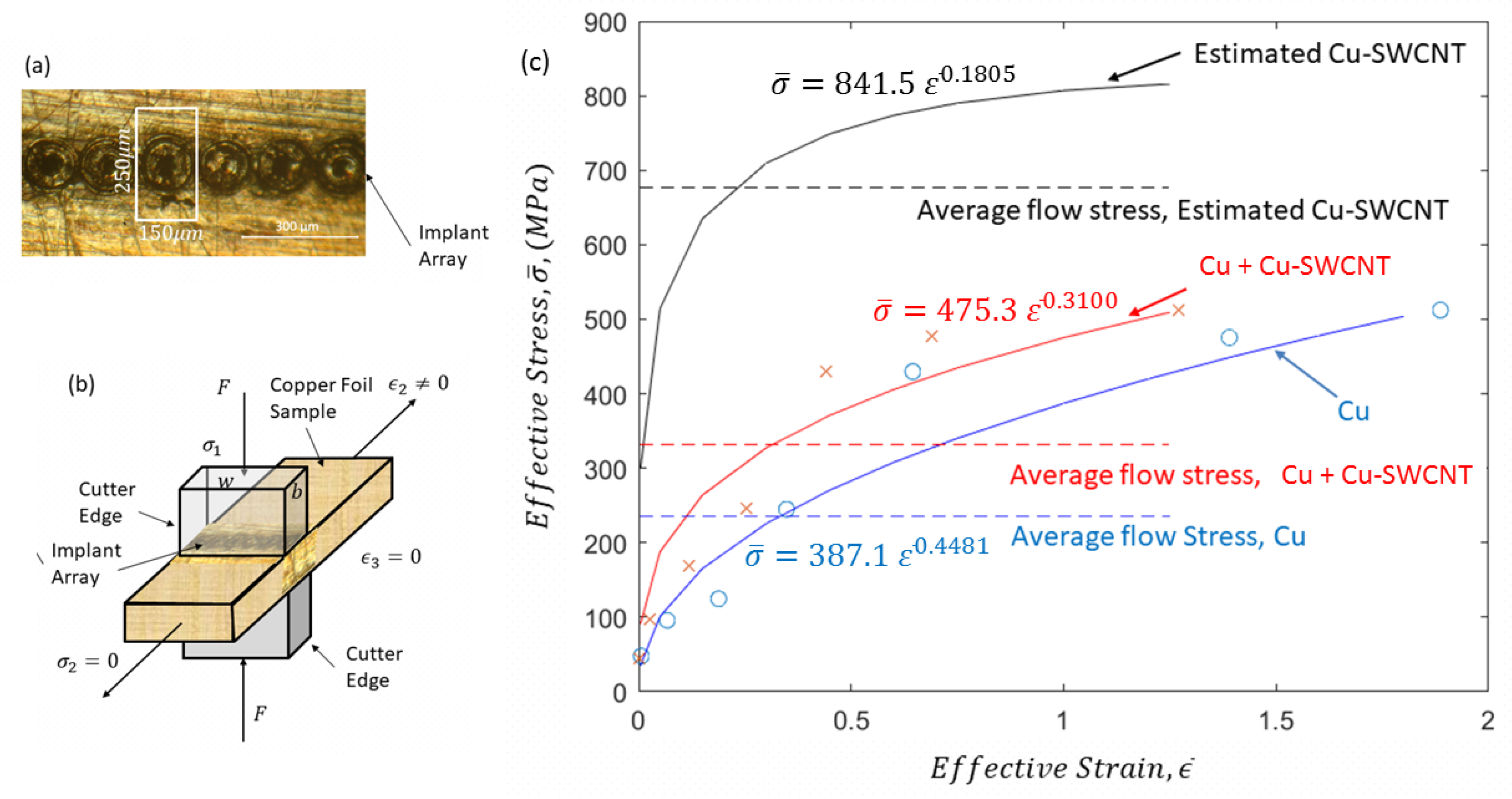
The standard tensile test is usually used to characterize the stress–strain behavior of a large sample with homogeneous properties. However, the standard tensile test cannot be used for the Cu-SWCNT implant because the size of the implant is too small and its property is not homogeneous. To overcome this difficulty, an array of Cu-SWCNT implants were produced (Figure 5a) and their collective stress–strain behavior with the copper substrate was measured using a specially designed plane strain compression test rig (Figure 5b) [16]. The actual stress–strain curve of Cu-SWCNT was then estimated using the rule of mixture. The plane stress–strain curve was converted to the effective stress and strain using the von Misses criterion, as presented in Figure 5c. The fitted power flow models are also provided in Figure 5c. Please refer to the work in [16] for details and the equations used for stress–strain curve conversion.
The effective stress and strain curve presented in Figure 5c provides a stress–strain curve similar to those by the standard tensile test with one major difference. Because there was no fracture during the compression test, the ductility, toughness, and the ultimate strength data are not available from the compression test result. They need to be estimated based on the plasticity theory.
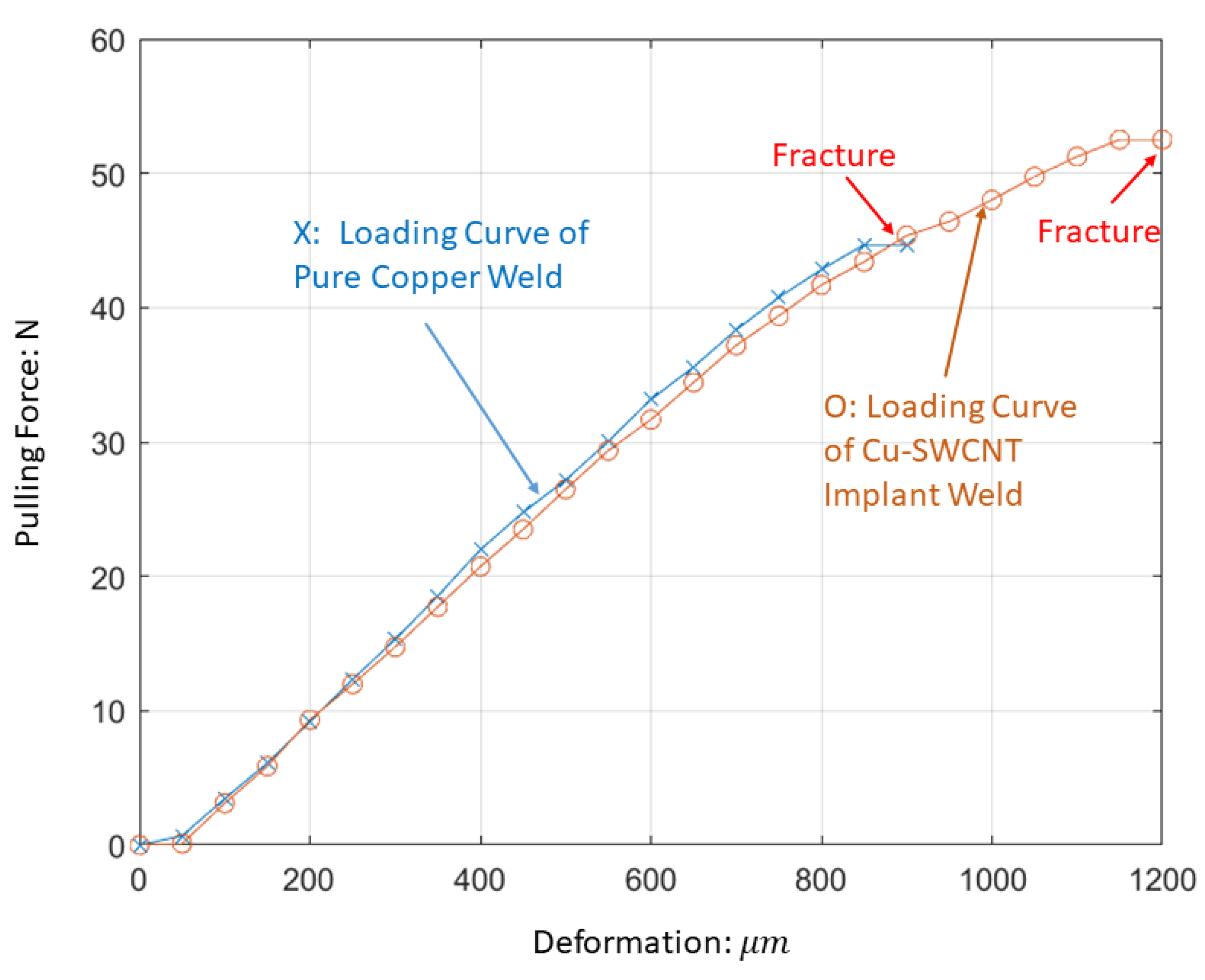
The strain-hardening exponent of the power flow model predicts the true strain at necking in the standard tensile test. Because the stress at necking is also the ultimate strength of the material, the ultimate strength of the Cu-SWCNT implant is estimated based on the stress at which the strain is equal to the exponent value. The ultimate strengths are thus estimated to be 270, 330, and 618 MPa for the copper substrate, the copper/implant array, and Cu-SWCNT nanocomposite, respectively. The published ultimate strength of annealed copper typically is 210 MPa, which is lower than that of the copper sample. This is because the copper sample is made from a copper foil which had been rolled and hardened. The test data show that the ultimate strength improvement is 229% (=618 MPa/270 MPa) or 294% (=618 MPa/210 MPa).
If we calculate the strength improvement of the nanocomposite based on the average flow stress for strain up to 1.25, the Cu-SWCNT nanocomposite has an improvement of 288% (=676.8 MPa/235 MPa). Again, this improvement value is consistent with those of the hardness test, toughness tests, and the ultimate strength estimates.

1.5. Cost of Strength Improvement

The strength improvement of the Cu-CNT composite achieved by the dry process via powder metallurgy is typically up to 200% at a volume fraction of 20%. The cost of CNT is about $400 per gram, while it is $0.06 per gram for copper. The material cost alone for the Cu-CNT composite is $80 per gram, which is a 133,300% increase in cost but for only a 200% improvement in strength. The cost to strength improvement ratio is about 660 to 1.
For the Cu-SWCNT nanocomposite synthesized by the LTI process, the volume fraction is 0.23% [4]. The material cost is $0.93 per gram for the Cu-SWCNT nanocomposite, or 1550% increase in material cost for 300% improvement in strength. The cost vs. strength ratio is about 5 to 1.
The discussions from Section 1.1, Section 1.2, Section 1.3, Section 1.4 and Section 1.5 present a thorough and yet concise review of the synthesis of the Cu-SWCNT composite and its properties. The significant increase in the strength of copper surface opens up some potential applications previously hindered by the low strength of copper. This hard Cu-SWCNT nanocomposite is an ideal candidate for applications where excellent heat management, superior surface strength, and high wear resistance are required. The presented properties improvements justify the proposed applications for the Cu-SWCNT composite.

2. Methods

In this paper, two potential applications are considered: (1) high-performance and wear resistant electric contacts to withstand extremely high number of on–off operations, and (2) spot welding of copper to form high strength weld at small weld size for a low heat affected zone.
The first application for electric contacts takes advantage of the rare improvements in both the hardness and toughness of the Cu-SWCNT composite, as discussed in Section 1.2, Section 1.3 and Section 1.4. When a material is hardened, its ductility typically is reduced. As a result, the toughness could be reduced. A material with a substantially lowered toughness is not suitable for applications with impact loading. A material used as electric contacts need to be impact and wear-resistant, along with a high electric conductivity and other properties [17].

2.1. Application of Cu-SWCNT Composite for Wear Resistant Electrical Contacts

The contact resistance of electric contacts is related to the contact area [18]. It is impossible to achieve 100% contact between two mating metal surfaces because the surfaces are never perfectly smooth due to the existence of micro-scale asperities. In electrical contacts, surfaces meet only at these asperities, occupying only a fraction of the total contact area. As electrical contacts go through loading and unloading cycles during switching, the impact and frictional forces cause plastic deformation and wear at the asperities, known as fretting, which could increase the contact resistance [17,18].
As discussed in Section 1, high volume fraction of CNTs in a Cu-CNT composite could reduce the electric conductivity substantially. Because only 0.23% volume fraction is used in the synthesis of the Cu-SWCNT implant, it is expected that its electric conductivity does not deteriorate substantially from that of pure copper, according to the authors of [13]. Note that for the application of electric contacts, the contact resistance is more critical than the electric conductivity of bulk material. The electric conductivity of the Cu-SWCNT composite was not investigated experimentally in this paper. The focus is on the change of the contact area of the electric contacts.
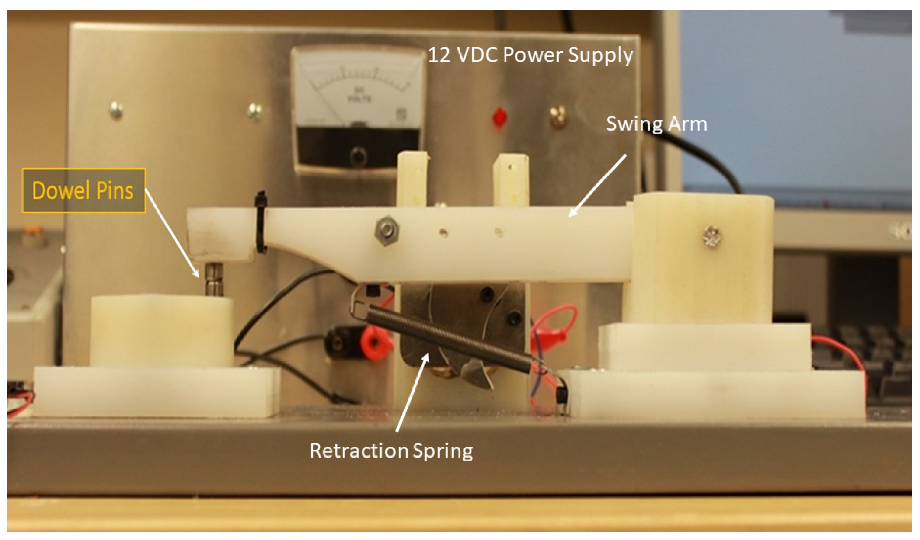
An impact test rig was fabricated to investigate the impact resistance of the nanocomposite, as shown in Figure 6. This rig can apply cyclic impact loading to copper plates with the Cu-SWCNT implants. The rig contains two hardened steel dowel pins for striking samples. The bottom dowel pin is fixed, while the upper dowel pin is attached to a swingable arm. The arm is controlled by a cam and driven by a 12 VDC electric motor. Once the arm reaches its maximum height, determined by the cam profile, a spring attached to the arm will bring it down to strike the lower pin. The rate and the impact force can be controlled by the height to which the arm was raised and the tension of the spring.
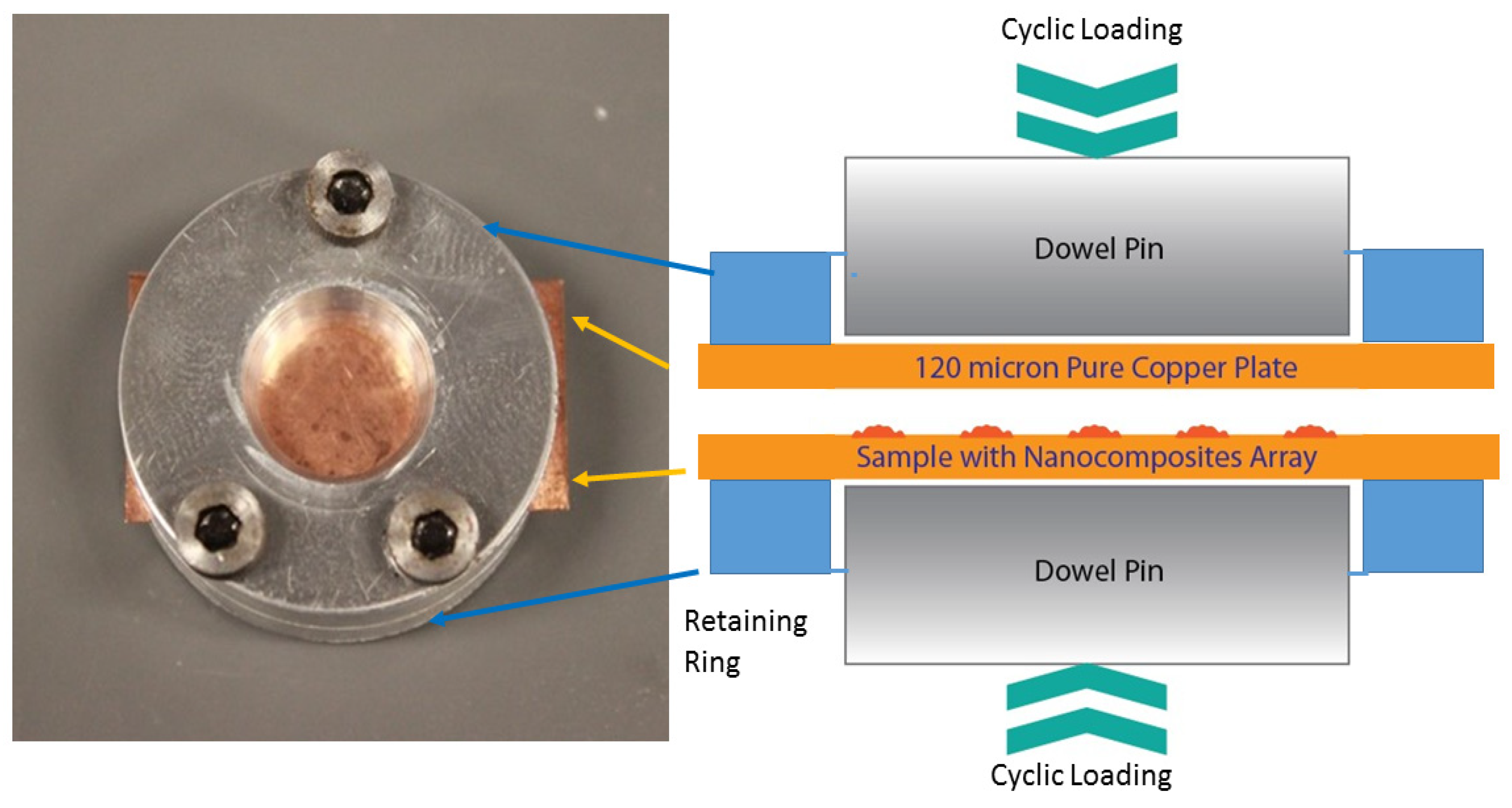
A copper foil imbedded with the Cu-SWCNT implants is mated with a pure copper foil without implants as a pair of electric contacts. The samples were held in place by a fixture made by two retaining rings, as shown in Figure 7. A 5 by 5 array of Cu-SWCNT implants were produced onto a 120 µm copper foil using the LSI process (Figure 1). These implants were spaced apart by 750 µm. The samples were cleaned after the LSI process with alcohol to remove SWCNTs residues. After that, they were hand-polished with cotton swabs soaked with 1 µm diamond polishing slurry. The same cleaning process is also applied to the mating pure copper foil.
The impact tests were carried out for 200, 500, 1000, and 2000 impact cycles. For each number of impact cycles, two or three samples were tested. In total, over 400 Cu-SWCNT implants underwent the impact cycles. It is cost prohibitive to scan the profiles of all the implants and their corresponding mating surfaces. Two or three Cu-SWCNT implants were chosen for profile measurements for each sample. The impact test results are presented in Section 3.1.

2.2. Application of Cu-SWCNT for High-Strength Spot Welding

The application of the Cu-SWCNT implant as spot weld takes advantage of its high strength and high ductility. The motivation of this application is to produce weld of high strength so that large size welds are not needed.
Copper is notoriously difficult to weld with a laser because of its very high reflectivity, well over 99%, for infrared laser beams. If extreme care is not taken to keep the reflected laser beam from entering the laser’s delivery optical fiber, the laser could be damaged. High-power laser welding of copper to achieve high penetration depth is even more difficult because a large amount of heat is involved to cause dimensional distortion and higher risk to the laser equipment. By keeping the weld small but strong, the heat distortion is kept low to achieve higher precision.

2.2.1. Laser Spot Welding Process Using Cu-SWCNT Implants

The high strength spot weld is in fact a Cu-SWCNT implant, created with the same LSI process (Figure 1), except that melting laser pulse duration is longer at 3 ms to achieve a higher implant depth. When pure copper samples were joined, no micro-holes were drilled and only the 3 ms laser pulse was used to generate the spot weld.
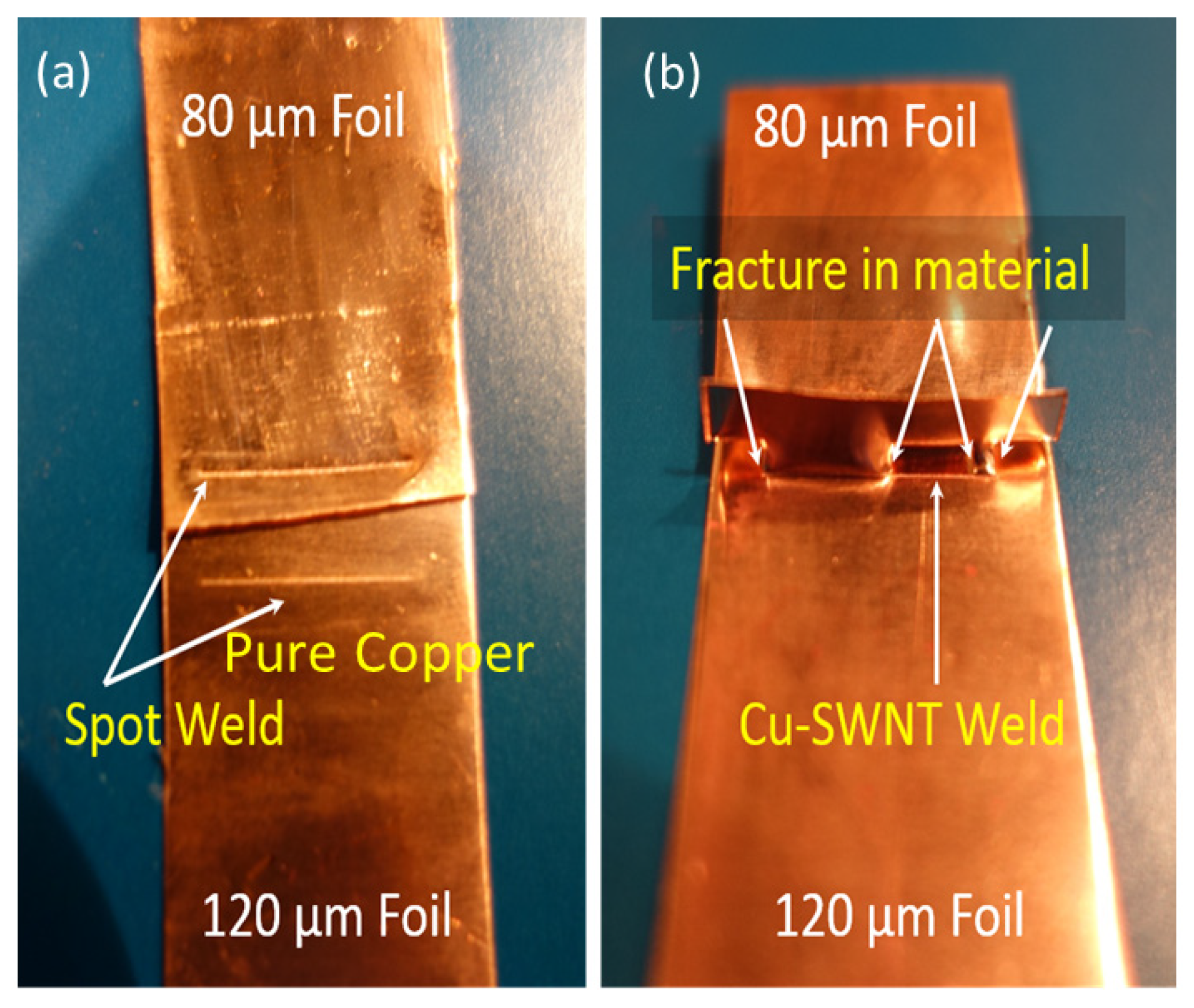
This unique laser spot welding process was applied to join a copper foil at 800 µm thickness to another foil at 120 µm thickness. The copper samples are 35 mm × 20 mm. These foil samples were spot welded together with 5 mm overlap and with the thinner copper foil placed on top. An array of 70 spot welds, each 150 µm in diameter, were created on the samples. From the work in [4], it is clear that the spot weld does not penetrate to the bottom of the second foil at 120 µm thickness.
It should be noted that the spot welds are not overlapped to avoid re-melting of the Cu-SWCNT implants. For pure copper welds, the same weld configuration is used for direct strength comparison. According to the authors of [19], non-overlapping spot welds also help to prevent failures of spot welds due to, for example, porosities [19]. This makes the strength test more consistent to characterize the actual weld strength.

2.2.2. Test Rig for Weld Strength Characterization via Lap-Shearing

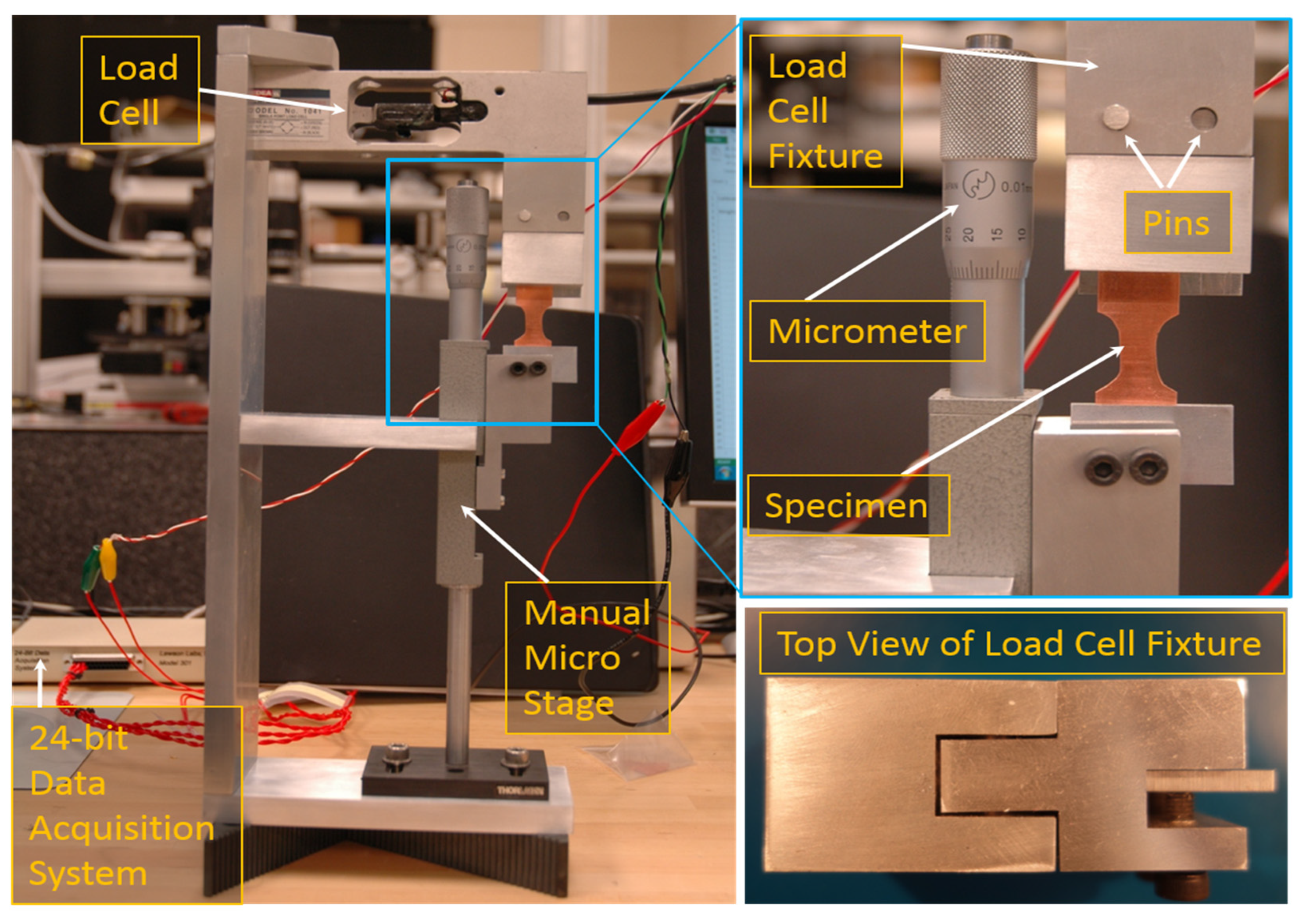
A test rig to investigate the weld strength was constructed using a load cell and a micro-positioning stage (Figure 8). To overcome misalignment, the load fixture was assembled using steel pins with clearance fit. This allowed the load fixture to align itself so that the welds are kept along the center axis of loading. Loading was applied to the specimen by manually tightening the adjusting screw of the microstage. Through tightening the micro-stage, the welded copper foils are pulled apart until fracture due to shearing. Therefore, this test is denoted as the lap-shear test in this paper.
The load cell is made by Tedea-Huntleigh, which is a single-point load cell (Model 1041). Its load capacity is 540 N. Its signal output resolution is 2 mV/V and it has 5000 maximum number of intervals. This allows the load cell to measure the loading force with a resolution of 0.107 N. The load cell output is sampled by a Lawson Labs Model 301 24-bit data acquisition system.

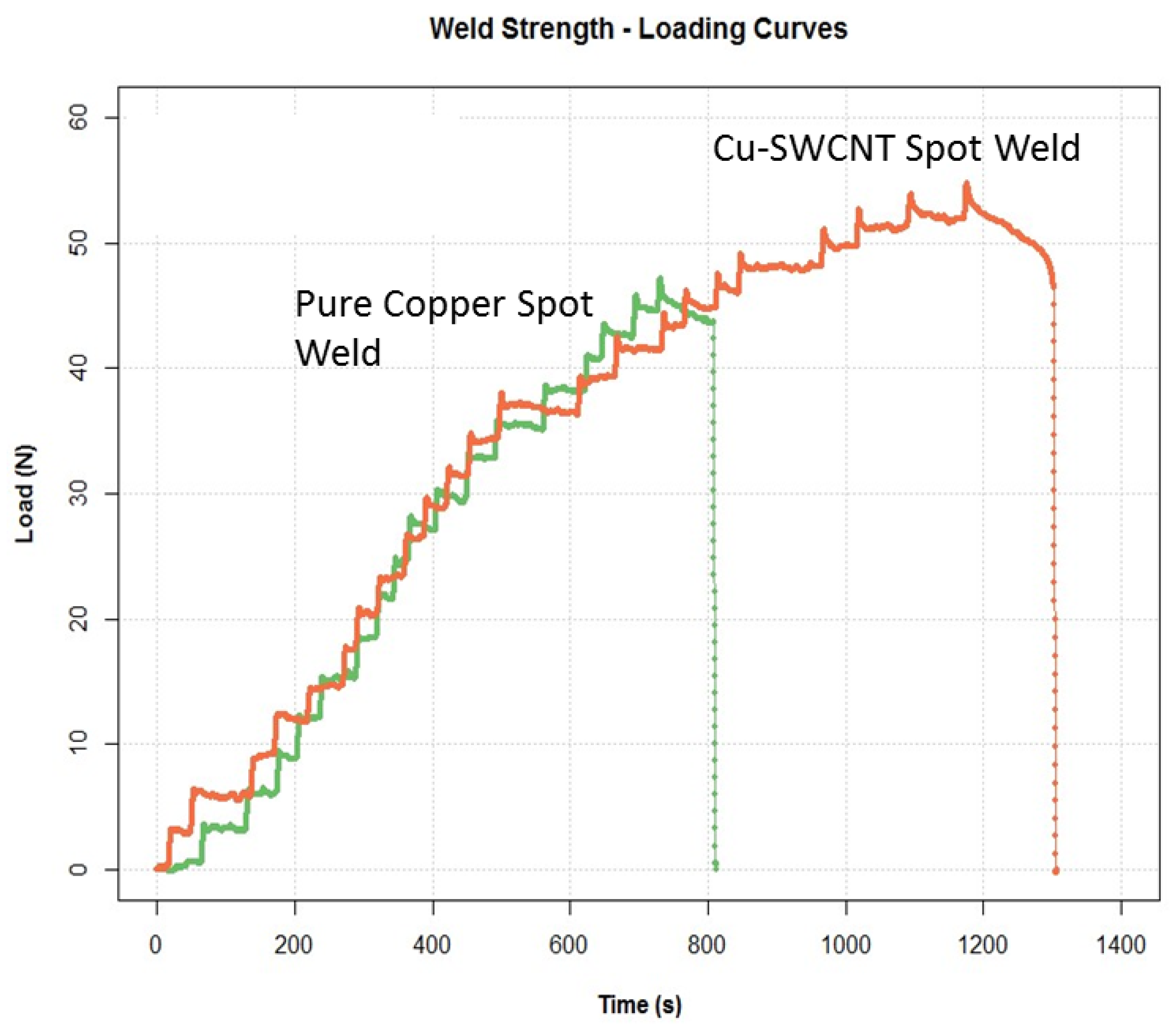
2.2.3. Weld Strength Characterization Tests

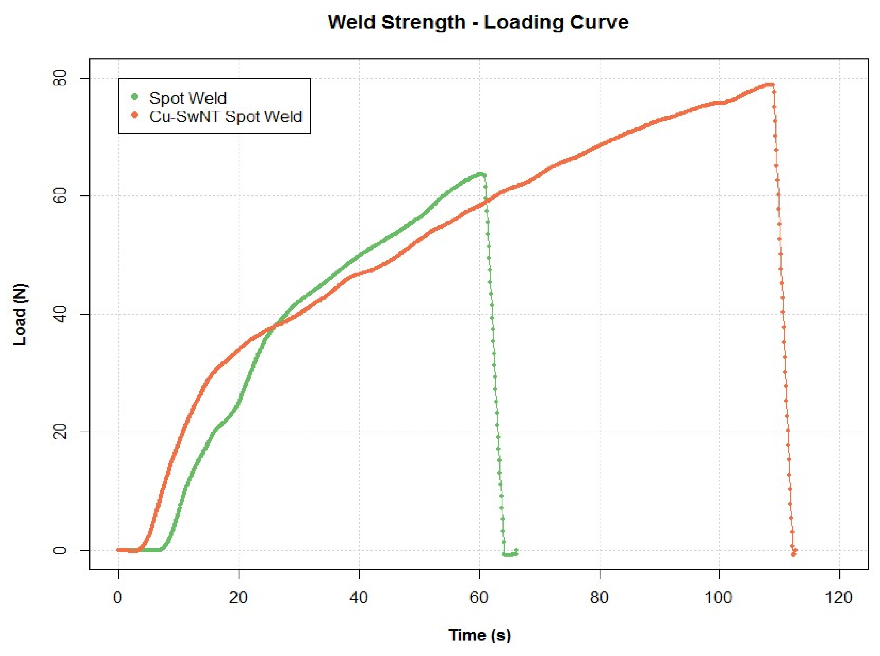
Two modes of increasing loading were applied by the test rig of Figure 8. The first mode was to increase the stretching force continuously. The second mode was to stretch the sample in fixed steps, in which the loading was allowed to stabilize before tightening the micro-stage again. The results of weld strength tests are presented in Section 3.2.

3. Results

The impact test results for the electric contacts are presented in Section 3.1, while the results for the spot welding in Section 3.2. The test results are presented to prove the feasibility of the proposed applications.

3.1. Results of Cyclic Impact Tests

A white light interferometer was used to measure the sample surface profile after a certain number of impact loading. The specimen surface must be reflective for the white light interferometer to measure it correctly. Moreover, if the profile has steep slopes, the instrument may fail to measure those slopes, again, due to poor light reflection. As a result, for a concave surface, some regions inside the cavity may not be reflective enough to allow accurate profile scanning. It is expected that the profile measurement would exhibit large variations. The objective of the surface profile scanning is to determine how the profile would change and progress. Two or three samples were scanned for each loading cycles and two or three scans across the profile were conducted. Only one scanned profile is presented in each number of impact cycles in this paper.

3.1.1. Surface Profiles before Impact

Figure 9 shows the surface profile of one of the nanocomposite implants before the cyclic impact loading. Profile measurements were taken on three different paths across the sample, but only one of the images from the instrument is shown in Figure 9. Peak–Valley (PV) values for these locations ranged from 6.205 µm to 7.464 µm and RMS values ranged from 1.184 µm to 1.774 µm.
Note that the white light interferometer plots the measured profile in green line, as shown in Figure 9, but the green line often is not continuous depending on the reflection from the profile, as discussed above. A faint line was added to trace the green line for better visualization.
From Figure 9, the Cu-SWCNT implant appears to be a bump over the copper foil substrate with an average height about 5.5 µm. In fact, the Cu-SWCNT implant is more like an iceberg imbedded into the copper substrate, with only a small portion of the implant appearing above the copper substrate surface.

3.1.2. Surface Profiles after 200 Cycles

Figure 10 shows the measured surface profiles of a Cu-SWCNT implant and the indentation formed on the pure copper foil after 200 cycles of impact loading. Because the Cu-SWCNT composite is two to three times stronger than pure copper, it is expected that the Cu-SWCNT will retain its form while an indentation would form on the pure copper foil, confirmed by Figure 10. The PV values for the implant from two profile measurements are from 6.656 µm to 8.106 µm, while the RMS values are from 1.472 µm to 2.147 µm. The PV values for the indentations on the pure copper are from 9.032 µm to 11.039 µm, while the RMS values are from 1.348 µm to 2.391 µm. Note that, as discussed above, the measurements for concave surfaces by white light interferometer are more difficult and could demonstrate more variations. The height of the Cu-SWCNT implant is about 4 µm, while the depth of the cavity on the pure copper foil is over 8 µm. These two measurements likely are incorrect. First, the scan path through the Cu-SWCNT did not pass through the center, making the height measurement lower, compared with Figure 9. Second, due to the sharp cavity, the depth measurement likely is not accurate.
Note that the area surrounding the Cu-SWCNT implant was deformed but the Cu-SWCNT implant maintained its profile with little changes.

3.1.3. Surface Profiles after 500 Cycles

Figure 11 shows the measured surface profiles of a Cu-SWCNT implant and the indentation formed on the pure copper foil after 500 cycles of impact loading. Additional impacts apparently deepened the cavity on the pure copper foil. The PV values for the implant from two profile measurements are from 6.659 µm to 8.697 µm, while the RMS values are from 1.337 µm to 3.404 µm. The PV values for the indentations on the pure copper are from 9.816 µm µm to 10.835 µm, while the RMS values are from 2.366 µm to 3.101 µm.
The cavity in Figure 11 might appear to be substantially wider than the one in Figure 10. In fact, the cavity in Figure 10 has an opening diameter about 120 µm versus 135 µm in Figure 11. The appearance in difference is due to the horizontal scale, which was determined by the scan path length. The scan path for the Cu-SWCNT was slight off the center but less compared with Figure 10. The height of the implant is 5.5 µm, similar to the height before impact.

3.1.4. Surface Profiles after 1000 Cycles

Figure 12 shows the measured surface profiles of a Cu-SWCNT implant and the indentation formed on the pure copper foil after 1000 cycles of impact loading. Additional impacts apparently deepened the cavity on the pure copper foil. The PV values for the implant from two profile measurements are from 6.083 µm to 7.777 µm, while the RMS values are from 1.556 µm to 2.076 µm. The PV values for the indentations on the pure copper are from 6.700 µm µm to 7.921 µm, while the RMS values are from 1.300 µm to 2.491 µm.
As discussed above, the measurements of the indentation depth appear to be more accurate due to better light reflection for a wider cavity. The opening diameter of the cavity in Figure 12 is 230 µm and the depth is 6 µm. In fact, the depth of the cavity should not become shallower after more impacts; it was likely due to the scanning path across the cavity is more off center in Figure 12. As discussed above, it is very difficult to scan at the same path due to the positioning of the samples are different each time when the sample was removed from the test rig and placed on the white light interferometer.

3.1.5. Surface Profiles after 2000 Cycles

Figure 13 shows the measured surface profiles of a Cu-SWCNT implant and the indentation formed on the pure copper foil after 2000 cycles of impact loading. Additional impacts apparently deepened the cavity on the pure copper foil. The PV values for the implant from two profile measurements are from 6.259 µm to 12.453 µm, while the RMS values are from 1.521 µm to 3.992 µm. The PV values for the indentations on the pure copper are from 9.437 µm µm to 10.319 µm, while the RMS values are from 1.924 µm to 2.752 µm.
Note that the profile of the indentation starts to resemble that of the Cu-SWCNT after 2000 impact cycles. The scanning paths across the implant and the cavity profiles were near the middle; therefore, the measured profiles can be used for direct comparison. The PV values reported in Figure 13 are 10.293 and 10.149 µm, respectively, and fairly matched. The height of the implant and the depth of the cavity are both at 9.25 µm, according to Figure 13. The base of implant has a diameter of 180 µm versus 200 µm opening diameter of the cavity.
To confirm the observation regarding the profiles of Figure 13, the samples were examined by a Zeiss inverted optical microscope. The optical microscope images are presented in Figure 14. It is confirmed that after 2000 impact cycles, the Cu-SWCNT transferred its profile to the pure copper surface, while the Cu-SWCNT implant essentially retained its original profile. This indicates that hardness of implants was indeed much higher than that of pure copper, as discussed in Section 1.2.

3.1.6. Surface Profiles Summary

The PV values measured by the white light interferometer for all samples and scanning paths are plotted in Figure 15 to show the progression of the profiles due to impact. As discussed above, the large variations of PV measurements were due to the profile randomness, scanning paths, and light reflection quality. The average values of the PV values were calculated and plotted in Figure 15 to demonstrate the trend of the profile progression with respect to the number of impact cycles. Figure 15 confirms that after 1000 impact cycles, the profiles of the implant and the cavity start to match each other, in terms of averages.

3.2. Results for Spot Weld Strength Tests

Figure 16 shows the images of two pure copper foils after they were pulled apart by the lap-shear test. They were initially joined by laser spot welding without SWCNTs (Figure 16a) and with SWCNTs (Figure 16b), respectively.
It is observed that the foils welded by Cu-SWCNT implants fractured at the ends of spot weld line, indicating Cu-SWCNT welds have a higher strength than the copper foil substrate. On the other hand, the foils welded without SWCNTs fractured at the weld.
Because the high strength of Cu-SWCNT, the joined foil set might fail at the substrate, observed in the initial study, the foil specimen was redesigned to ensure that the stress at the weld interface was higher than other regions of copper foil sample, as shown in Figure 17. By joining the foils at the section with a reduced width, the lap shear test could ensure the maximum shear stress occur along the weld line. The same sample geometry was also used for the welding of copper foils without SWCNT for comparison.

3.2.1. Results of the Lap-Shear Tests with Continuous Loading

Figure 18 shows the loading curves during the continuous loading lap-shear test. The adjustment screw was turned to tighten the test sample continuously. Note that Figure 18 is plotted as the measured force versus time, not strain. During continuous loading, we did not know exactly the displacement of the rig to pull the samples apart at any time. Furthermore, the strain rate was not controlled precisely, which might affect the strength measurement.
No failure in the foil away from the weld was observed, which was the design objective of Figure 17. Fracture loads for pure copper spot welds and Cu-SWCNT welds are 63.65 N and 78.85 N, respectively. These test results show that Cu-SWNT welds are 23.88% higher in strength than the pure copper weld. However, note that this does not indicated that the Cu-SWCNT weld itself is only 23.88% stronger because the failure occurs at the area surrounding the Cu-SWCNT weld.
In addition, direct comparison of the loading curves for both samples at the same time axis should be avoid because the actual strains for the same time instant likely were different. Figure 18, nevertheless, is a preliminary test to prove that the Cu-SWCNT implants are indeed stronger as expected.

3.2.2. Weld Strength Test of Copper Specimens with Controlled Strain Increments

In this test, samples were pulled apart with controlled strain increments. Samples were prepared by similar procedures mentioned before but 300 µm apart. The loading was applied in steps, not continuously. In each step, displacement of 50 µm is applied by tightening the adjustment screw of the microstage. The load cell output was allowed to stabilize to a steady-state value before tightening to the next strain level.
Figure 19 shows the results from these tests. The loading curves in Figure 19 for pure copper welds and Cu-SWCNT implants match each other until the pure copper weld fails, different from those shown in Figure 18. This is indicative why controlled strain increments is important for a better controlled study of weld strength. Extracting the deformation information from Figure 19, proper force versus deformation curves (similar to engineering stress versus engineering strain curve) can now be constructed as shown in Figure 20.
For the pure copper weld, the copper foils separated at 900 μm deformation (after 18 tightening steps) and 44.7 N pulling force, while for the weld of Cu-SWNT implants, they were 1200 μm (after 24 tightening steps) and 52.5 N, respectively. As a result, the foils with the Cu-SWNT weldment sustained 18% higher tensile force and 33% higher in plastic deformation. The results for a higher strength for Cu-SWCNT implants is consistent with the results in Figure 18. However, 33% higher in plastic deformation before fracture for the Cu-SWCNT is quite unexpected. We discuss this result in the next section.

4. Discussion

Several issues are discussed regarding the test results presented in Section 3.

4.1. Data Variations

Note that PV measurements by the white light interferometer are prone to variations, similar to common surface roughness measurements. In addition, the scanning path across the profile could not kept exactly the same, which added more variations to the profile measurement. Therefore, the PV values are used for qualitative study, not for high quantitative precision.

4.2. Profile Progression and Wear due to Impacts

From the impact loading tests for electric contacts, it can be observed that by impacting the Cu-SWCNT implant against the pure copper caused copper to form a cavity, conforming the implant profile. It appears that, after 1000 cycles, the profile of the indentation took the form of the Cu-SWCNT implant (Figure 15). This result is desirable because when the two mating surfaces conform to each other, it results in a substantially higher contact area. Higher contact area is beneficial for achieving higher electric conducting performance because it reduces the contact resistance for a longer life.
In addition, few signs of fretting were observed as shown by Figure 13 because after 2000 impact cycles, the Cu-SWCNT implant maintains its profile. By comparing the heights of the surface profiles of the Cu-SWCNT implants in Figure 9, Figure 10, Figure 11, Figure 12 and Figure 13, it clearly shows that the Cu-SWCNT implant suffers very little wear even after 2000 impact loading. This result is not unexpected because the counter part of the Cu-SWCNT implant during the impact test was pure copper.
No fracture was observed for the Cu-SWCNT implant in Figure 15 from the optical microscope images. This is achieved due to the excellent toughness property presented in Figure 4.

4.3. Different Mating Pair Consideration

Note that the impact test did not put one Cu-SWCNT implant against another because it is not desirable to have two convex profiles as mating surfaces due to reduced contact area. If Cu-SWCNT implants were used as mating contacts, they likely would retain their profiles because the deformation would occur at the substrate as in Figure 10 and Figure 11.

4.4. Loading Mode Consideration in the Lap Shear Test

Even though the loading curves in Figure 19 are plotted with respect to time, as recorded by the data acquisition system, it becomes obvious that this test is better controlled. Both loading curves are nearly identical until the pure copper weld started to fail. Figure 20 confirms this observation.

4.5. Spot Weld Strength Comparison

The Cu-SWCNT weld was able to sustain an additional 300 µm deformation before it failed. While the force increase is only 18%, and not very impressive, close examination shows that the copper foils were torn apart at the heat affected zone around the Cu-SWNT weld. In other words, the Cu-SWNT weld did not fail because its strength is much higher, as presented in Section 1. Figure 19 and Figure 20 do not imply that the Cu-SWCNT weld is only 18% stronger.

4.6. Failure Mode of the Cu-SWCNT Spot Weld

Failures occurring in the neighborhood of the weld, not the weld itself, are also common in continuous welding of carbon steels. This is because the carbon steel weld underwent rapid cooling to have a quenching effect for a higher strength, while the area near the weld has an annealing effect for a lower strength. The high deformation (related to ductility) of Figure 19 and Figure 20 is actually related to the copper substrate surrounding the Cu-SWCNT implant, not an indication that the Cu-SWCNT implant has a higher ductility than pure copper.

4.7. Application of the Cu-SWCNT Spot Welding for Other Configurations

In addition to welding thin foils as shown in this paper, another potential application of Cu-SWCNT implants is for butt joint welding of thick plates. With thick plates, the failure would more likely happen at the weld, not the substrate, to take full advantage of the improved strength of the Cu-SWCNT implant.

5. Conclusions and Future Work

In this paper, we presented two potential applications for the Cu-SWCNT implants synthesized by the Laser. Both applications take advantage of the superior strength and toughness of the Cu-SWCNT implants. The feasibilities of the Cu-SWCNT implant for these two applications were confirmed with custom-designed test rigs.
The first application is related to creating long lasting electric contacts. The result shows that the Cu-SWCNT nanocomposite is highly wear-resistant. When a pure copper foil is mated with a copper foil with the Cu-SWCNT implants, the contact area increases after over 1000 impact cycles because the copper foil starts to conform to the profile of the Cu-SWCNT implant. An increase in contact area will reduce the contact resistance. The actual electric conductivity performance of the electric contact will be investigated in the future work by adding a 120 VAC or 230 VAC power supply to the test rig. The impact tests will then be conducted with the electricity engaged and disengaged as in an actual relay.
The second application is to apply the Cu-SWCNT implants for high strength spot welding of copper. The results show that the Cu-SWCNT implants are substantially stronger spot weld than pure copper. Smaller but stronger weld can provide the same weld strength while reducing the power requirement of the laser and the thermal distortion of welding for a higher-dimensional precision. The future work will focus on applying this high strength spot weld for welding thicker plates.
The specially designed test rig for the weld strength characterization is a new contribution, providing a method to test small and non-homogenous samples not suitable for a standard tensile test machine.

Author Contributions

J.F.T. was responsible for the original ideas of the tests, analysis, and the writing of the first and final drafts. N.R. was responsible for conducting tests, data analysis, and writing of many parts of the manuscript. S.D.M. was responsible for editing and suggestions to improve the data analysis. All authors have read and agreed to the published version of the manuscript.

Funding

This research was funded by NSF DMII Grant #0550734 as well Engineering On Line, Department of Mechanical and Aerospace Engineering of NCSU, the CHA!N group, and the Knowledge Foundation of Sweden.

Acknowledgments

Special thanks to Aaron Dale for his design and construction of the impact rig for the electric contact application. The FIB and SEM tests were performed at the Analytical Instrumentation Facility (AIF) at North Carolina State University, which is supported by the State of North Carolina and the National Science Foundation (award number ECCS-1542015). The AIF is a member of the North Carolina Research Triangle Nanotechnology Network (RTNN), a site in the National Nanotechnology Coordinated Infrastructure (NNCI). The authors also would like to acknowledge Mangesh Champhekar for his work in nanoindentation tests on SWCNT–Cu samples. The work was performed in part at Wendy E. Krause Lab at Textile Engineering, Chemistry, & Science Department in North Carolina State University.

Conflicts of Interest

The authors declare no conflict of interest.

References

  1. Agarwal, A.; Bakshi, S.R.; Lahiri, D. Carbon Nanotubes: Reinforced Metal Matrix Composites; CRC Press: Boca Raton, FL, USA, 2011. [Google Scholar]
  2. Bakshi, S.R.; Lahiri, D.; Agarwal, A. Carbon nanotube reinforced metal matrix composites—A review. Int. Mater. Rev. 2010, 55, 41–64. [Google Scholar] [CrossRef]
  3. Rajule, N. Laser Synthesis and Characterization of Copper-Single Walled Carbon Nanotubes Nanocomposites. Ph.D. Thesis, North Carolina State University, Raleigh, NC, USA, 2014. [Google Scholar]
  4. Tu, J.F.; Rajule, R.; Molian, P.; Liu, Y. Laser synthesis of a copper–single-walled carbon nanotube nanocomposite via molecular-level mixing and non-equilibrium solidification. J. Phys. D Appl. Phys. 2016, 49, 495301. [Google Scholar] [CrossRef]
  5. Dong, S.R.; Tu, J.P.; Zhang, X.B. An investigation of the sliding wear behavior of Cu-matrix composite reinforced by carbon nanotubes. Mater. Sci. Eng. A 2001, 313, 83–87. [Google Scholar] [CrossRef]
  6. Dong, S.; Zhang, X. Mechanical Properties of Cu-based Composites Reinforced by Carbon Nanotubes. Trans. Nonferr. Met. Soc. China 1999, 9, 457–461. [Google Scholar]
  7. Arai, S.; Osaki, T.; Hirota, M.; Uejima, M. Fabrication of Copper/Single-Walled Carbon Nanotube Composite Film with Homogeneously Dispersed Nanotubes by Electroless Deposition. Mater. Today Commun. 2016, 7, 101–107. [Google Scholar] [CrossRef]
  8. Kim, K.T.; Cha, S.I.; Hong, S.H.; Hong, S.H. Microstructures and tensile behavior of carbon nanotube reinforced Cu matrix nanocomposites. Mater. Sci. Eng. A 2006, 430, 27–33. [Google Scholar] [CrossRef]
  9. Zhang, X.; Xu, Y.; Wang, M.; Liu, E.; Zhao, N.; Shi, C.; Lin, D.; Zhu, F.; He, C. A powder-metallurgy-based strategy toward three-dimensional graphene-like network for reinforcing copper matrix composites. Nat. Commun. 2020, 11, 2775. [Google Scholar] [CrossRef] [PubMed]
  10. Yang, Y.L.; Wang, Y.D.; Ren, Y.; He, C.S.; Deng, J.N.; Nan, J.; Chen, J.G. Single-walled carbon nanotube-reinforced copper composite coatings prepared by electrodeposition under ultrasonic field. Mater. Lett. 2008, 62, 47–50. [Google Scholar] [CrossRef]
  11. Guiderdoni, C.; Estournès, C.; Peigney, A.; Weibel, A.; Turq, V.; Laurent, C. The preparation of double-walled carbon nanotube/Cu composites by spark plasma sintering, and their hardness and friction properties. Carbon 2011, 49, 4535–4543. [Google Scholar] [CrossRef] [Green Version]
  12. Jean-François Silvain, J.-F.; Veillère, A.; Lu, Y. Copper-Carbon and Aluminum-Carbon Composites Fabricated by Powder Metallurgy Processes. In Journal of Physics: Conference Series, Volume 525, Eurotherm Seminar 102: Thermal Management of Electronic Systems; IOP Publishing: Bristol, UK, 2016. [Google Scholar]
  13. Uddin, S.M.; Mahmud, T.; Wolf, C.; Glanz, C.; Kolaric, I.; Volkmer, C.; Höller, H.; Wienecke, U.; Roth, S.; Fecht, H.J. Effect of size and shape of metal particles to improve hardness and electrical properties of carbon nanotube reinforced copper and copper alloy composites. Compos. Sci. Technol. 2010, 70, 2253–2257. [Google Scholar] [CrossRef] [Green Version]
  14. Tu, J.F.; Rajule, N.; Liu, Y.; Martin, J. Nanostructure diffraction analysis of a copper/single walled carbon nanotube nanocomposite synthesized by laser surface implanting. Carbon 2017, 113, 1–9. [Google Scholar] [CrossRef] [Green Version]
  15. Tu, J.F. TEM Nano-Moiré Pattern Analysis of a Copper/Single Walled Carbon Nanotube Nanocomposite Synthesized by Laser Surface Implanting. J. Carbon Res. 2018, 4, 19. [Google Scholar] [CrossRef] [Green Version]
  16. Tu, J.F.; Rajule, N.; Mun, S.D. Novel Characterizations of Mechanical Properties for a Copper/Single-Walled Carbon Nanotube Nanocomposite Synthesized by Laser Surface Implanting. C J. Carbon Res. 2020, 6, 10. [Google Scholar] [CrossRef] [Green Version]
  17. Slade, P.G. Electrical Contacts: Principles and Applications; CRC Press: Boca Raton, FL, USA, 2013. [Google Scholar]
  18. Sawada, S.; Shimizu, K.; Shimada, S.; Hattori, Y. Prediction of Electrical Contact Resistance of Tin-Plated and Silver-Plated Terminals. SEI Tech. Rev. 2010, 71, 37–43. [Google Scholar]
  19. Chao, Y.J. Ultimate strength and failure mechanism of resistance spot weld subjected to tensile, shear, or combined tensile/shear loads. J. Eng. Mater. Technol. 2003, 125, 125–132. [Google Scholar] [CrossRef]
Figure 1. The laser surface implanting (LSI) process for synthesizing the copper–single-walled carbon nanotube (Cu-SWCNT) nanocomposite. The LSI process contains (a) microhole drilling, (b) laser melting, and (c) rapid solidification. This is a revised image based on the work in [2].
Jcs 05 00087 g001
Figure 2. (a) TEM image; TEM images obtained by JEOL 2010F STEM, of a Cu-SWCNT sample. The moire fringes are indicated by green arrows, while discernable SWCNT clusters in nanosizes are indicated by the yellow arrow. (b) The corresponding refraction index image of subfigure (a). (c) TEM image of a annealed pure copper sample. (d) The corresponding refraction index image of subfigure (c). This figure is a compiled image based on the works in [14,15].
Jcs 05 00087 g002
Figure 3. (a) Micro-hardness test for pure copper. (b) Micro-hardness test for a Cu/SWCNT implant sample. (c) Nano-hardness test pure copper. (d) Nano-hardness test near the edge of a Cu-SWCNT implant. (e) Nano-hardness test near the center of the implant. This figure is a compiled image based on the works in [4,16].
Jcs 05 00087 g003
Figure 4. The craters and their depths bombarded by focused ion beam (FIB) and the equivalent toughness of the Cu-SWCNT nanocomposite at different locations of an implant. This figure is a compiled image based on the work in [16].
Jcs 05 00087 g004
Figure 5. (a) An array of Cu-SWCNT nanocomposite on a copper foil. (b) Plain–strain compression test for a copper foil with a Cu/SWCNT implant array. (c) Measured and estimated stress–strain curves for pure copper, Cu and Cu-SWCNT, and Cu-SWCNT only, respectively. This figure is a compiled image based on the work in [16].
Jcs 05 00087 g005
Figure 6. A test rig was designed to apply cyclic impact loading to a pair of contacts.
Jcs 05 00087 g006
Figure 7. A pair of retaining rings hold the samples together so that cyclic loading can be applied.
Jcs 05 00087 g007
Figure 8. Weld strength test rig, similar to a standard tensile tester but the tensile force is applied by stretching the test specimen via adjusting the micro-stage.
Jcs 05 00087 g008
Figure 9. Surface profile measurement by a white light interferometer of a Cu-SWCNT implant before impact loading.
Jcs 05 00087 g009
Figure 10. Surface profile measurements: (a) a Cu-SWCNT implant and (b) the indentation formed on the pure copper after 200 cycles of impact loading.
Jcs 05 00087 g010
Figure 11. Surface profile measurements: (a) a Cu-SWCNT implant and (b) the indentation formed on the pure copper after 500 cycles of impact loading. The indentation is now wider, compared with the one in Figure 10.
Jcs 05 00087 g011
Figure 12. Surface profile measurements: (a) a Cu-SWCNT implant and (b) the indentation formed on the pure copper after 1000 cycles of impact loading. Some debris due to damages might start to appear based on the images above.
Jcs 05 00087 g012
Figure 13. Surface profile measurements: (a) a Cu-SWCNT implant and (b) the indentation formed on the pure copper after 2000 cycles of impact loading. The indentation profile starts to resemble the Cu-SWCNT implant profile.
Jcs 05 00087 g013
Figure 14. Images by optical microscope for the Cu-SWCNT implant and the indentation after 2000 cycles. These images confirm the profile measurement done by the white light interferometer.
Jcs 05 00087 g014
Figure 15. Profile progression vs. impact cycles.
Jcs 05 00087 g015
Figure 16. Copper foil samples after the lap-shear test: (a) copper foils joined by laser without SWCNT and (b) copper foils joined by Cu-SWCNT implants.
Jcs 05 00087 g016
Figure 17. Geometry for lap-shear test specimen.
Jcs 05 00087 g017
Figure 18. Weld strength test of the specimens with continuous loading.
Jcs 05 00087 g018
Figure 19. The results of the lap-shear test with controlled strain increments.
Jcs 05 00087 g019
Figure 20. The loading versus deformation curves of the lap-shear test with controlled strain increments.
Jcs 05 00087 g020
Publisher’s Note: MDPI stays neutral with regard to jurisdictional claims in published maps and institutional affiliations.

