1. Introduction
Copper (Cu) and its alloys are widely used in the electrical power, petrochemical, transportation, and heavy machinery industries due to their excellent ductility and malleability, which make them well suited for these applications. However, certain limitations such as moderate hardness, limited wear resistance, and moderately low tensile strength can restrict their use in mechanically demanding or abrasive environments.
These shortcomings can be addressed by various alloy addition and thermomechanical processes, including cryogenic treatment and subsequent heat treatment, which modify the microstructure and significantly improve their functional performance.
Deep cryogenic treatment (DCT) [
1] is a thermal treatment process, where materials are subjected to extremely low temperatures, typically below −130 °C, often using liquid nitrogen, soaking, and warming. When the material is subjected to DCT, where changes begin in microstructure and which create internal stresses and lattice distortion, which results in the generation of dislocation density.
Heat treatment after deep cryogenic treatment (DCT) is essential for relieving internal stress, restoring ductility, and optimizing microstructure. These processes promote controlled grain growth, recrystallization, and dislocation annihilation, which enhance electrical conductivity. This combined approach (DCT + HT) provides a superior balance of properties [
1].
While initially cryogenic treatment was recognized for its benefits in tool steels to improve their performance and wear resistance, its application has expanded to a wide array of materials including steel and non-ferrous [
2] metals like copper, plastics, and composites.
Cryogenic treatment can influence metallurgical and structural properties. For instance, it can transform retained austenite into martensite in steels [
3], promote the formation of fine and uniform microstructures, and lead to the disappearance of vacancies and an increase in dislocations [
4], forming sub-grain boundaries and refining grains in materials like copper. These microstructural changes contribute to enhanced mechanical properties such as strength and hardness [
5], wear resistance [
6], toughness, and dimensional stability across various materials. Improving mechanical and tribological properties plays a vital role in advanced manufacturing [
7].
Research shows that cryogenic treatment on copper particularly deep cryogenic treatment (DCT), at temperatures as low as −196 °C using liquid nitrogen, has been proven to enhance the wear resistance and mechanical properties of materials such as creep resistance [
8], micro hardness, and strength [
9] of various metals and alloys.
Cryogenically treated copper electrodes, employed in Electrical Discharge Machining (EDM), have improved tool wear resistance, material removal rate, and surface finish [
10] compared to untreated electrodes.
Deep cryogenic treatment followed by heat treatment (DCT + HT) studies have reported a 7–12% improved tensile strength [
11] and hardness with refined grain structures. DCT + HT introduces a synergistic effect by combining cryogenic treatment with a controlled heat treatment process. This synergistic interaction promotes controlled grain refinement at optimal soaking durations, alleviates residual stresses, and thereby improves the mechanical properties, thermal conductivity, and electrical conductivity of copper [
12,
13].
Regarding electrical conductivity, Matthiessen’s rule states [
14] that total electrical resistivity is a sum of contributions from phonon scattering, lattice defects (dislocations, grain boundaries), and impurities.
Initially, cryogenic treatment was widely utilized for tool steels, alloys and in non-ferrous metal like copper. Systematic investigation in copper, particularly regarding fixed soaking durations in conjunction with low-temperature post-treatment, is notably less. Previous investigations frequently concentrate on cryogenic durations and assess either mechanical or electrical characteristics. Moreover, comprehensive correlations between microstructure and functional properties, especially electrical conductivity, are not reported across all soaking durations.
This study establishes clear correlations between grain evolution and the functional performance of copper. It provides a deeper understanding of the structure-property relationship in copper subjected to DCT and DCT + HT (post-heat treatment), across soaking durations ranging from 6 to 24 h, including a non-soaked condition termed as pure copper.
Advanced characterization techniques, including X-ray diffraction (XRD), Scanning Electron Microscopy–Electron Backscatter Diffraction (SEM–EBSD), High-Resolution Transmission Electron Microscopy (HR-TEM) and Raman spectroscopy, are used to analyze vibrational characteristics and lattice disorder in cryogenically treated copper, providing insights into defect structures.
2. Materials and Methods
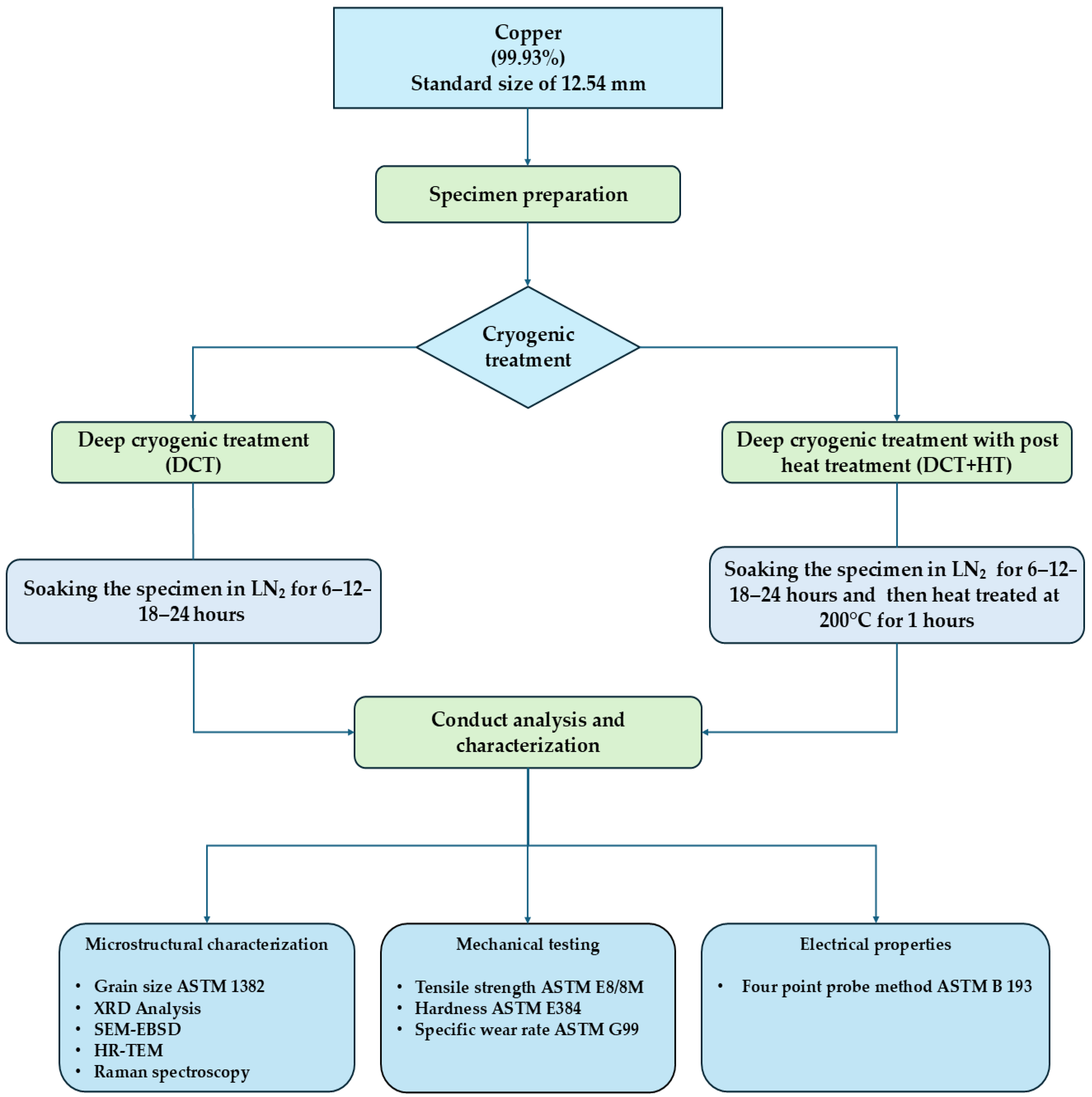
The material under study is 99.93% pure copper rods of 12.54 mm diameter. The Cu specimens are prepared as per the required standards and subjected to two cryogenic treatment routes, DCT and DCT + HT.
Figure 1 Provides detailed the process of cryogenic treatment and their characterization process. Each process is fully explained in experimental procedure. The specimen description is given in
Table 1.
2.1. Specimen Preparation
Tensile Strength: Copper rods were machined on a lathe to meet ASTM E8M [
15] standards, with dimensions of 6 mm diameter, 30 mm gauge length, and 6 mm radius filler.
Hardness: The samples for the hardness test were machined to 10 mm diameter and 10 mm length using a lathe, following ASTM E 384 [
16].
Specific wear rate: Determine the specific wear rate, samples were machined to a radius of 6 mm, diameter of 12 mm, and length of 60 mm as per ASTM G99 [
17].
Grain size: The samples were prepared to dimension of 10 mm in diameter and 10 mm in length. Samples were ground with emery paper (220 to 2000 grit size), then polished using diamond suspension and colloidal silica, followed by etching as per ASTM E3 [
18] standards.
Crystallite size and dislocation density: The copper rods were machined using wire cut machine and reduced to a dimension of 12 mm diameter and length of 5 mm.
Grain boundary and texture analysis: Samples with dimensions of 12 mm in diameter and 2 mm in length were prepared using a Wire Electrical Discharge Machining (WEDM) for SEM–EBSD analysis. The samples were ground with emery paper ranging from 220 to 2000 grit size, followed by rough polishing with diamond suspensions, and then fine polishing with colloidal silica to achieve a mirror finish. The samples were then electropolished using Struer’s electropolishing machine. The D2 electrolyte is employed and primarily composed of phosphoric acid H3PO4, ethanol, 1-propanol, water, and urea. A constant voltage of 13 V was applied, and continuous polishing was performed for 20 s to obtain a highly polished surface.
D-Spacing: The copper rod was prepared using a WEDM to a dimension of 3 mm diameter and thickness of 0.1 mm for HR-TEM analyses. Samples were ion milled with help of the Precision Ion Polishing System (PIPS).
Vibrational Intensity: The copper rod is machined using WEDM for the dimension of 12 mm diameter and length of 0.2 mm.
Electron mobility and conductivity: The copper rod is machined using WEDM for a dimension of 12 mm diameter and length of 0.2 mm.
2.2. Experimental Procedure
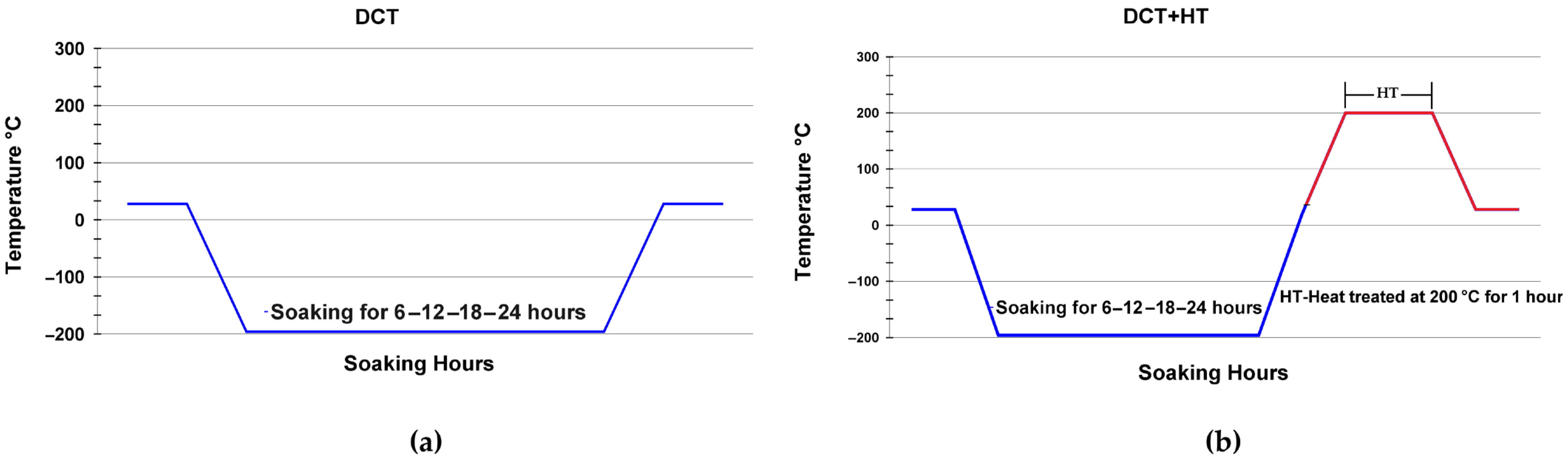
2.2.1. Deep Cryogenic Treatment (DCT)
Deep cryogenic treatment was conducted using liquid nitrogen (LN
2) stored in a Dewar flask to maintain a constant temperature of −196 °C. Pure copper specimens were soaked in LN
2 for four different durations of 6, 12, 18, and 24 h, respectively. After soaking, all specimens were slowly returned to room temperature before any further testing (
Figure 2a).
2.2.2. Deep Cryogenic Treatment + Heat Treatment (DCT + HT)
Another batch of specimens underwent the same DCT process as described above. After cryogenic treatment and returning to ambient temperature, these samples were subsequently heat treated at 200 °C for 1 h in a muffle furnace to enhance toughness and ductility [
19]. The specimens were then cooled to room temperature for evaluation [
20] (
Figure 2b).
2.3. Microstructural and Electrical Characterization
Microstructural images were captured using inverted optical microscopy. With help of microstructural images, grain size and grain count were evaluated using MIPAR software (version 5.2) [
21] employing a copper-specific segmentation recipe and following ASTM 1382 standards [
22].
X-ray diffraction (XRD) was performed using a Bruker D8 Advance diffractometer (Bruker Corporation, Billerica, MA, USA) with a Cu Kα radiation source (λ = 1.5406 Å), scanned from 5° to 90° at a 0.02° step size and 2°/min scan speed.
Using Scherrer’s formula, the crystallite size (D) [
23] is calculated.
where
D is the crystallite size (nm),
k is the Scherrer constant (0.94),
λ is the X-ray wavelength (1.5406 Å),
β is the full width at half maximum (FWHM) of the peak in radians, and
θ is the Bragg angle in degrees.
Lattice imperfections were evaluated by estimating the dislocation density (
) [
24].
To accurately estimate microstrain (ɛ) [
25], we used the Williamson–Hall method to separate the β value from size-related broadening.
SEM–EBSD analysis was performed on electropolished samples using a FEI QUANTA 250 FEG SEM (Thermo Fisher Scientific, Hillsboro, OR, USA) with a 0.15 µm step size. ATEX software (version 5.03) [
26] was used to generate grain boundary maps, pole figures, and inverse pole figures.
High-Resolution Transmission Electron Microscopy (HR-TEM) was conducted using a JEOL 200 microscope by JEOL Ltd., Tokyo, Japan. SAED patterns, along with bright and dark field images, were analyzed using CrysTBox (version 1.10) [
27] to extract interplanar d-spacings.
Raman spectroscopy was performed with a Renishaw Confocal Raman microscope (Renishaw plc, Gloucestershire, UK) using a 532 nm laser to assess vibrational modes and detect lattice distortions.
Finally, electrical conductivity (σ) and electron mobility (µ) of copper were measured using a four-point probe apparatus following ASTM B193 standards [
28].
The electrical conductivity (
σ) [
29] is calculated using the resistivity (
ρ)
Electron mobility (
) [
29] is estimated using this relation.
where
μ is the electron mobility (cm2/V·s),
n is the charge carrier concentration for copper (8.5 × 1028 m−3),
q is the electron charge (1.6 × 10⁻¹⁹ C), and
σ is the electrical conductivity (S/m).
2.4. Mechanical Property Assessment
Tensile strength was measured using a Tinius Olsen universal testing machine (Tinius Olsen, Horsham, PA, USA) with a strain rate of 1 mm/min [
30]. The cylindrical tensile specimens had a gauge length of 91 mm and a diameter of 6 mm. The X-direction refers to the longitudinal axis of the specimen, which is also the direction of the applied tensile load. The Y- and Z-directions correspond to the radial and circumferential directions, respectively, and are perpendicular to the loading axis. Hardness was assessed using a Vickers hardness tester [
31] (Mitutoyo Corporation, Kanagawa, Japan) under standard conditions. Specific wear rate [
32] was evaluated via a pin-on-disk tribometer, following ASTM G99 standards. Copper samples were rubbed against an EN 31(Ducom Instruments; Bangalore, India) steel disk (63 HRC) under a 20 N load, at 300 RPM, with a sliding distance of 564.5 m and a sliding speed of 1.8 m/s.
3. Results
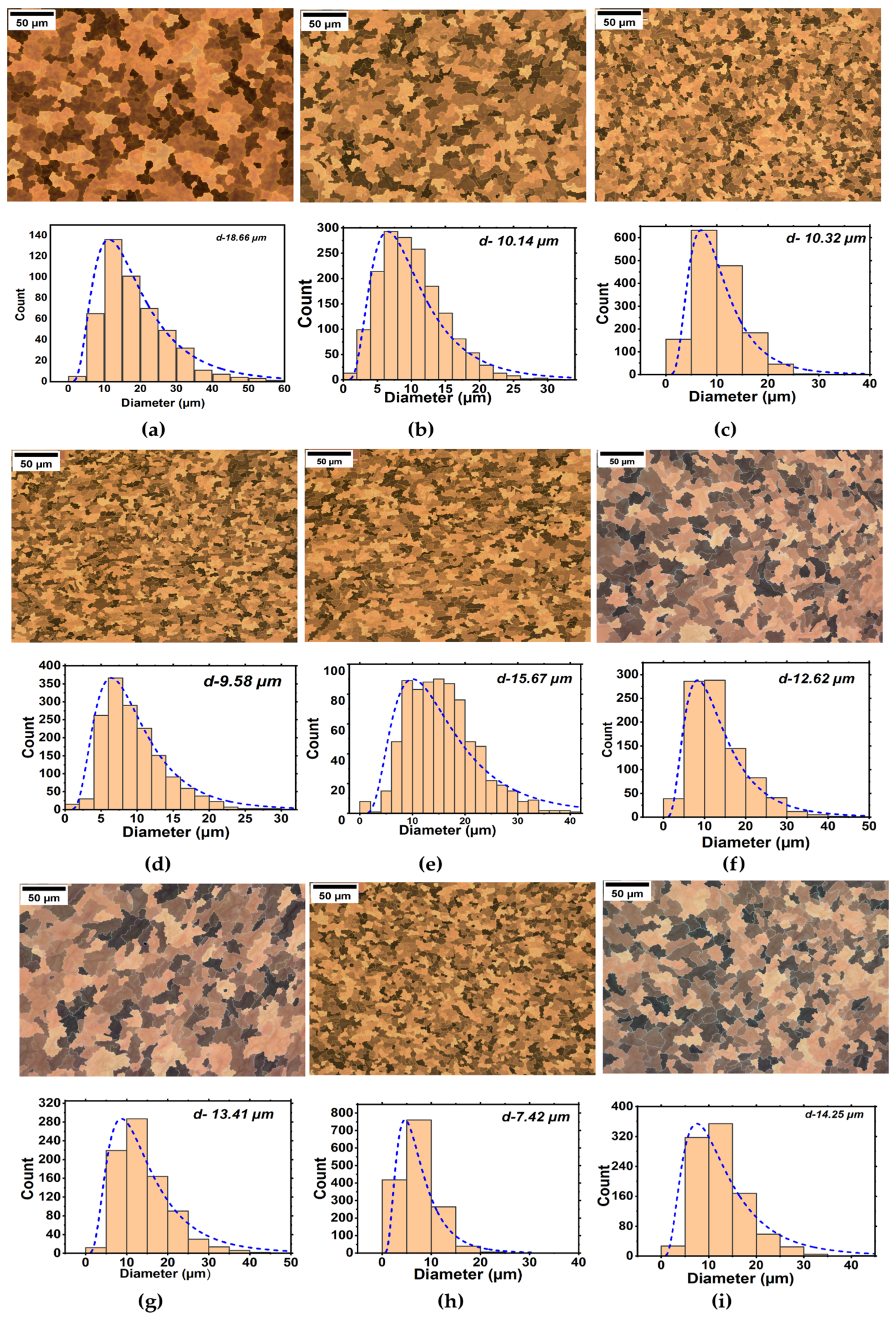
3.1. Grain Size
The grain size distribution and microstructural evolution across copper, DCT and DCT + HT specimens reveal clear trends in grain refinement and subsequent coarsening (
Figure 3). Copper exhibits the coarsest grains with an average size of 18.66 µm.
Upon applying DCT, significant refinement occurs, reducing the grain size to approximately 10.14 µm and 10.32 µm for 6 and 12 h of soaking and reaching a minimum of 9.58 µm at 18 h. However, further soaking for 24 h (DCT-24) led to grain coarsening, increasing the average size to 15.67 µm.
In contrast, the DCT + HT samples display a more nuanced behavior. While DCT + HT-6 and DCT + HT-12 showed a moderate grain sizes of 12.62 µm and 13.41 µm, respectively, DCT + HT-18 achieves the finest grain size of 7.42 µm indicating optimal refinement through the combined effects of cryogenic treatment and heat treatment.
However, further soaking for 24 h leads to grain coarsening, increasing the average size to 14.25 µm. This behavior indicates that prolonged thermal exposure reduces dislocation density and internal strain, which serves as driving forces for recrystallization and subsequent grain coarsening.
3.2. Crystallite Size, Dislocation Density and Microstrain
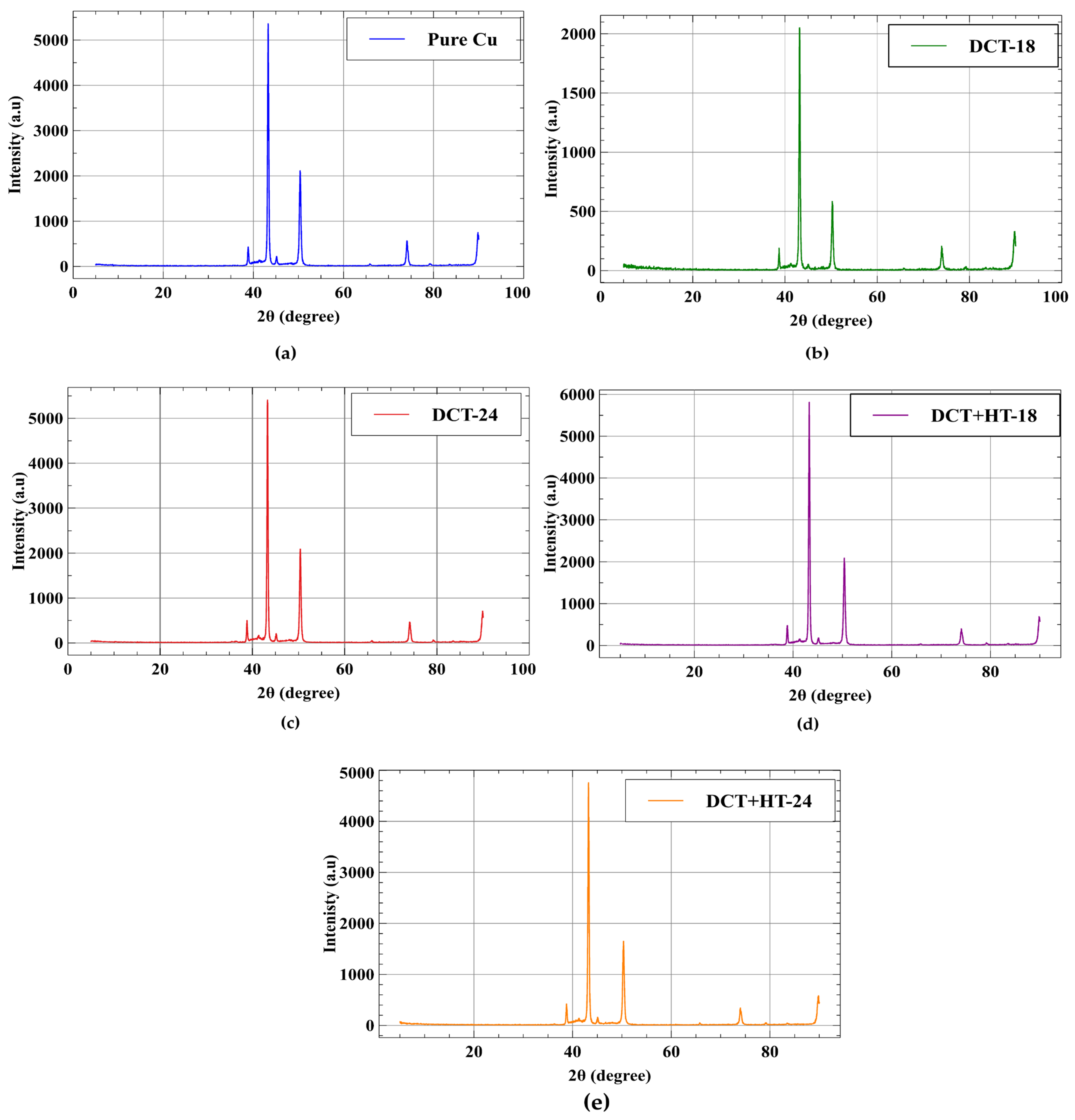
Based on the observed grain size and grain count, the soaking durations of 18 and 24 h for both treatments exhibited significant contrast and hence X-ray diffraction (XRD) analysis was performed on DCT-18, DCT-24, DCT + HT-18, and DCT + HT-24 to evaluate crystallographic changes, such as crystallite size and microstrain, contributing to the observed mechanical behavior are shown in
Table 2.
Figure 4 provides the x-ray profile line of copper.
Untreated copper has a crystallite size of 33.6 nm and a dislocation density of 8.86 × 10¹⁴ m−2. As the crystallite sizes decrease and dislocation density increase. A reduction in crystallite size is seen in DCT-18 and DCT + HT-18 specimen, with the smallest crystallite size achieved in DCT + HT-18 (31.7 nm) specimen. DCT-18 has a dislocation density of 9.35 × 10¹⁴ m−2, while DCT + HT-18 has a density of 9.95 × 10¹⁴ m−2.
The DCT-24 and DCT + HT-24 specimens exhibited crystallite sizes of 35.2 nm and 39.9 nm, respectively, exceeding that of untreated copper (33.6 nm). The DCT + HT-24 specimen shows the lowest dislocation density at 6.28 × 10¹⁴ m−2, leading to reduced mechanical performance.
Among the analyzed XRD results, DCT + HT-18 and DCT + HT-24 were found to exhibit the highest and lowest crystallite sizes, respectively, making them the most representative of peak and degraded performance. Consequently, these two specimens were subjected to detailed microstructural investigation via High-Resolution Transmission Electron Microscopy (HR-TEM) and Scanning Electron Microscopy–Electron Backscatter Diffraction (SEM–EBSD) to explore the grain boundary behavior.
3.3. Grain Boundary
Grain boundaries in copper are categorized based on their misorientation angles into low-angle grain boundaries (LAGBs) and high-angle grain boundaries (HAGBs) and the corresponding results are summarized in
Table 3. LAGB is defined by where the misorientation angles are less than 10°, typically indicate the presence of sub-grain structures formed through dislocation accumulation during recovery. In contrast, HAGBs, where the misorientation angles greater than 10°, are characteristic of recrystallized grains and serve as more effective barriers to dislocation motion.
An increased LAGB fraction, as observed in DCT + HT-treated samples, suggests formation of recovery and improved microstructural stability. This is reflected in the development of preferred orientations, particularly along the (111) and (112) planes, as confirmed by pole figure and inverse pole figure analysis. These orientations are known to enhance electron mobility and mechanical strength in copper. Crystallographic texture was analyzed with help of captured pole figures and inverse pole figures (IPF) and are shown in
Figure 5. The mrd values presented in the pole figures were derived from a single scan using ATEX software, which does not provide statistical error estimates.
Pure Cu has an LAGB fraction of 39.4%, after the cryogenic treatment LAGB increased to 61.3% and 60.2% for DCT + HT-18 and DCT + HT-24, respectively. This significant rise indicates structural modifications induced by the cryogenic treatment, resulting in a dominance of LAGB. Conversely, HAGB decreased to 38.7% and 39.8% in DCT + HT-18 and DCT + HT-24, showing a refinement in grain structure [
33].
The pole figure analysis in (111) orientation, DCT + HT-18 exhibits a 7.5% decrease in pole figure intensity compared to pure copper, whereas DCT + HT-24 shows a 2.6% increase. The higher intensity observed in DCT + HT-24 [
33], suggests enhanced crystallographic alignment along the (111) direction, which contributes to improved electrical conductivity due to reduced grain boundary scattering [
34]. The (100) intensity increases in both treated samples, with a 3.8% rise in DCT + HT-18 and 2.7% in DCT + HT-24, supporting better texture alignment for electron transport.
The (110) orientation shows a slight increase in pole figure intensity, from 3.15 mrd in pure copper to 3.32 (5.4% increase) mrd in DCTH-18 and 3.39 (7.6% increase) mrd in DCTH-24 and this trend suggests a slight reorientation effect due to DCT + HT. For the (112) orientation, the intensity increases from 2.03 mrd in pure copper to 2.21 mrd in DCTH-18 (8.9% increase), while DCTH-24 shows a near-constant value of 2.02 mrd (0.5%decrease).
3.4. D-Spacing Values
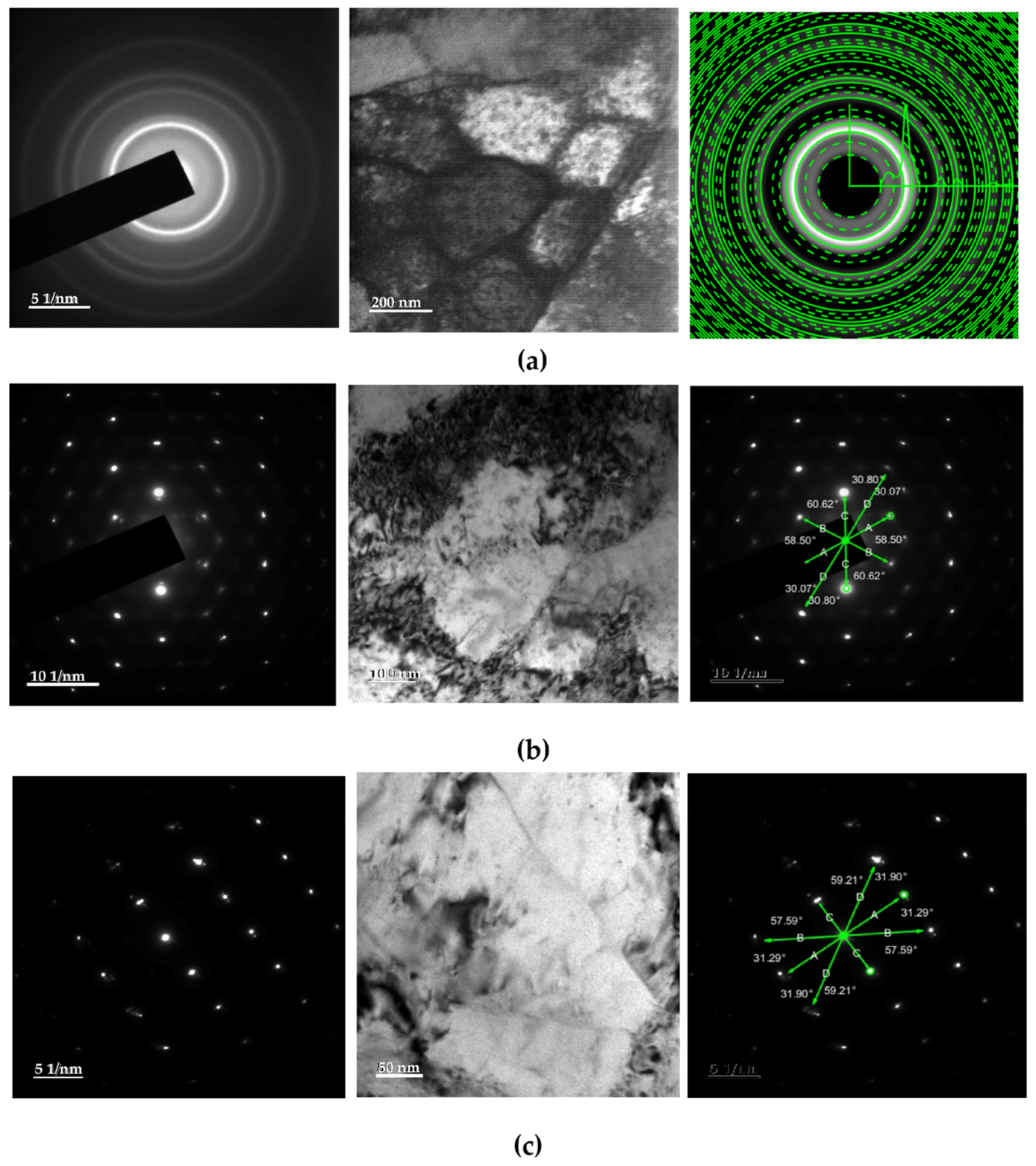
Using HR-TEM, diffraction images of cryogenically treated copper were captured and analyzed with help of CrysTbox. The SAED pattern of the pure cu sample shows broad and diffused concentric rings
Figure 6a, characteristic of a polycrystalline material with randomly oriented grains and minimal internal lattice strain. D-spacing values for copper were measured using CrysTbox across planes (111), (022), and (004), yielding 0.230 nm, 0.142 nm, 0.121 nm, and 0.090 nm, respectively.
Similarly, for DCT + HT-18 specimen, d-spacing values are evaluated along the (1 −1 1) zone axis, exhibiting a reduced values are 0.123 nm, 0.123 nm, 0.126 nm, and 0.0724 nm and comparing the pure copper has 0.230 nm, 0.142 nm, 0.121 nm, and 0.090 nm. This reduction indicates lattice distortion and internal strain induced by the combined effect of cryogenic and post-heat treatment processes.
Conversely, the DCT + HT-24 specimen, aligned along the [−4 0 5] zone axis, exhibited d-spacing values of 0.055, 0.0470, 0.0905 and 0.0478 nm.
The selected area electron diffraction (SAED) pattern for DCT + HT-18 shown in
Figure 6b, where it displays a partial ring formation and moderately defined spots with noticeable angular variations such as 30.07°, 30.80°, 58.50°, and 60.62° indicating a semi-ordered structure with residual lattice strain and higher dislocation density.
In contrast, the SAED pattern for DCT + HT-24 is characterized by sharp, discrete, and symmetrically arranged diffraction spots, with angles such as 31.29°, 31.90°, 57.59°, and 59.21°. This high degree of crystallographic symmetry and spot clarity suggests a well-ordered lattice with minimal defects, resulting from recovery or partial recrystallization processes.
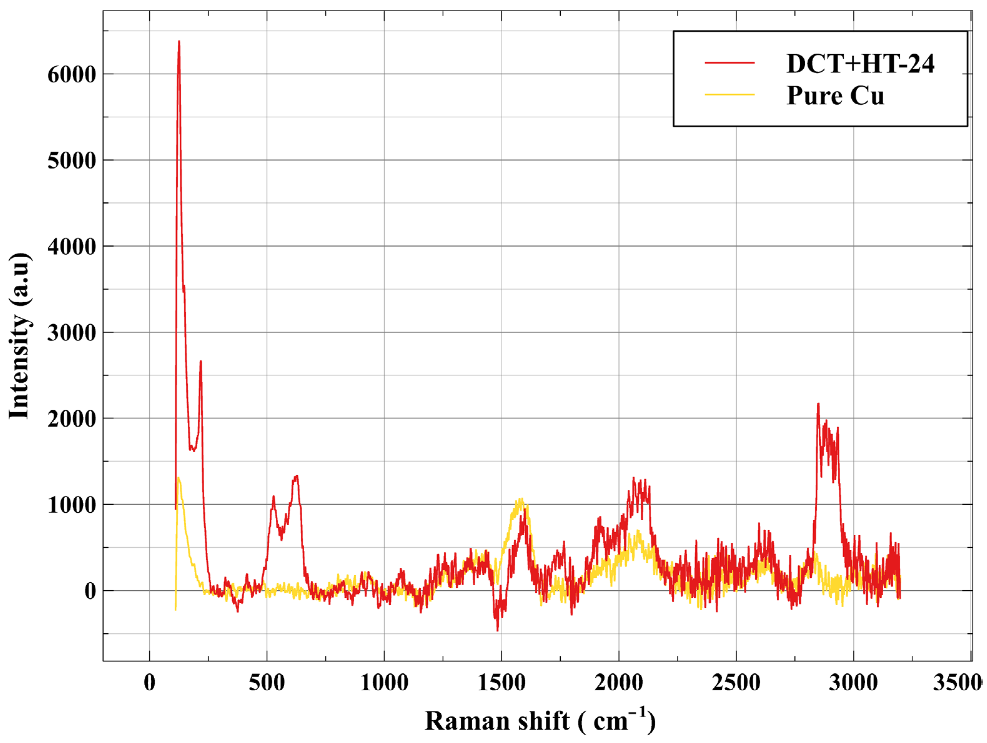
3.5. Vibrational Intensity
Figure 7 Raman spectra of pure copper and DCTH-24 measured across a shift range of 0 to 3500 cm
−1. DCTH-24 exhibits significantly higher intensity across the entire spectrum compared to pure copper, particularly in the low-wavenumber region below 500 cm
−1 and approximately 2900–3100 cm
−1, suggesting enhanced lattice vibrations. Copper intensity reaches up to 2.0 × 10
3 a.u., while DCT + HT-24 peaked to 6.0 × 10
3 a.u.
3.6. Conductivity and Electron Mobility
The electrical conductivity and electron mobility of copper samples are shown in
Table 2. Copper exhibited a conductivity of 4.4 × 10
7 S/m and an electron mobility of 32.50 cm
2/V·s and after DCT and DCT + HT, both properties are significantly increased. In DCT-18 specimen conductivity and mobility increases to 5.21 × 10
7 S/m and 38.25 cm
2/V·s.
Further improvement is observed in the DCT-24 specimen, with a conductivity of 5.47 × 10⁷ S/m and a mobility of 40.35 cm2/V·s. The DCT + HT-18 sample demonstrates a conductivity of 4.95 × 10⁷ S/m and a mobility of 36.30 cm2/V·s, while the DCT + HT-24 sample achieves the highest conductivity of 7.09 × 10⁷ S/m and electron mobility of 52.08 cm2/V·s.
3.7. Tensile Strength, Hardness, and Specific Wear Rate
The mechanical and tribological properties of pure copper and cryogenically treated specimens (DCT and DCT + HT) were evaluated for tensile strength, hardness, and specific wear rate measurements as presented in
Table 4. Copper exhibited a tensile strength of 299 MPa, which significantly improved after DCT, peaking at 343 MPa for 18 h of soaking (DCT-18) and the strength slightly decreased to 330 MPa for 24 h of soaking (DCT-24), suggesting a saturation effect.
In DCT + HT, the maximum tensile strength of 330 MPa was observed in specimen soaked for 18 h (DCT + HT-18), slightly lower than DCT-18. Beyond 18 h of soaking, the strength decreases to 294 MPa at 24 h.
Pure copper shows the coarse grain structure with an average grain size of 18.67 µm, corresponding to the hardness value of 82 HV and leading to a specific wear rate of 13.1 × 10⁻¹⁰ m3/Nm, showing poor tribological performance. In specimens subjected to deep cryogenic treatment (DCT), a substantial improvement of hardness was seen after 6 h of soaking, with the hardness increasing to 122 HV and remain stable between 12 and 18 h of soaking. However, a decline was noted at 24 h of soaking. For specimens subjected to DCT + HT, the hardness of copper increased from 82 HV to 18 h of soaking, reaching 111 HV and 115 HV, respectively. The most substantial improvement is observed in the DCT + HT-18 specimen, and this specimen achieves the finest grain structure, with an average grain size of just 7.42 µm, with highest hardness of 149 HV, and lowest specific wear rate of 7.73 × 10⁻¹⁰ m3/Nm. After 24 h of soaking, the DCT + HT-treated specimen exhibited a decrease in hardness to 105 HV. At DCT-24 and DCT + HT-24 specimens hardness declined to 98 HV and 105 HV and wear rates increased to 9.51 × 10⁻¹⁰ m3/Nm and 10.21 × 10⁻¹⁰ m3/Nm, respectively.
4. Discussion
4.1. Microstructural Evolution During Various Soaking Hours
Various Soaking hours reveals a gradual transformation in their mechanical properties. Each specified soaking hour marks a significant stage wherein noticeable alterations in performance are observed. These transformations can be attributed to the microstructural changes that occur over different soaking hours. By analyzing the grain size measurements presented in
Figure 3, we can gain insight into how the soaking house influences the microstructure of the specimens. These observations align with mechanical trends previously noted, where both DCT-18 and DCT + HT-18 exhibited peak hardness and wear resistance, confirming that optimal grain refinement directly contributes to superior mechanical performance. The observed increase in average grain size at 24 h of soaking is attributed to grain coarsening driven by recovery and grain growth mechanisms. As the soaking hours extends, the accumulated dislocations and internal stresses induced by cryogenic treatment begin to reduce and which reduces the dislocation density and microstrain. This reduction promotes increased grain boundary mobility, and results in grain coarsening.
4.2. Dislocation Density and Its Impact on Mechanical Properties
The DCT + HT-18 specimen showed the highest peak broadening, showing a significant reduction in crystallite size and high dislocation density, which aligns with its superior mechanical properties. In contrast, the DCT + HT-24 specimen showed narrower diffraction peaks, suggesting grain coarsening and a drop in dislocation density, indicative of partial recovery or over-saturation effects at extended treatment durations.
Dislocation density influences mechanical properties such as strength, hardness, and grain size. Higher density hinders electron movement, thereby decreasing the mobility in copper. Conversely, lower density results in a larger crystallite size with fewer grain boundaries, enhancing electron mobility [
35], as seen in the DCT + HT-24 specimen.
4.3. Grain Boundary Characteristics and Crystallographic Texture
HAGB and LAGB characteristics and crystallographic texture influence the microstructure of copper samples. In the DCT + HT specimens (DCT + HT-18 and DCT + HT-24), there is a higher percentage of low-angle grain boundaries (LAGB) and a corresponding reduction in high-angle grain boundaries (HAGB) [
36] are seen. This shift is typically improving crystalline and reducing the internal strain, which can enhance properties like mobility.
Electrical conductivity measurements were performed using the four-point probe method on copper samples. The surface orientation of the sample was not specifically controlled or characterized and is assumed to be randomly oriented. Improvement of conductivity was observed in DCT + HT specimens. Generally (111) and (100) plane facilitate electron transport in face-centered cubic (FCC) materials like copper [
37]. Plane (111) is the most densely packed and has lowest surface energy, when the intensity of the (111) orientation increases and making it ideal for improved mobility [
14,
38]. The (100) orientation also supports good electron movement but is slightly less effective than (111) due to its lower atomic density.
Form the pole figure analysis (111) orientation is dominant and DCT + HT-24 specimen exhibits the highest (111) intensity [
39] of 8.78 (mrd), indicating a stronger preferred orientation favorable for electron transport [
40,
41]. The DCT + HT treatment promote more stable microstructures with higher percentage of low-angle grain boundaries (LAGBs) and stronger (111) texture both which are beneficial for improving electron mobility [
36,
38].
At (100) orientation pole figure shows an increase in intensity from 4.44 mrd in pure copper to 4.61 mrd and 4.56 mrd in the DCT + HT-18 and DCT + HT-24 specimens. This incremental rise suggests a reorientation in (100) crystallographic orientation. This texture evolution forms after cryogenic treatment with post heat treatment due to the recovery and recrystallization process and results in realignment of grains leading to the observed enhancement in the (100) texture and promoting reorientation.
In contrast, higher-index planes such as (110) and (112) which are structurally less favorable for electron mobility have lower intensities, while DCT + HT-24 specimen has 2.02 mrd and pure copper has 2.03 mrd. Therefore, enhancing (111) and (100) [
38] while minimizing (110) and (112) components is desirable for maximizing electrical conductivity in FCC materials like copper [
42].
The inverse pole figure (IPF) intensity values along the X, Y, and Z directions provide insight into the crystallographic texture and its effect on the mechanical behavior of copper after DCT + HT treatment. In the X-direction, both DCT + HT-18 and DCT + HT-24 samples exhibited a slightly reduced intensities (2.21 mrd) compared to pure copper (2.42 mrd), indicating a more randomized grain orientation along this axis. In the Y-direction, DCT + HT-18 displays the highest intensity (2.71 mrd), suggesting a weak preferential alignment that could influence anisotropic deformation. Conversely, DCT + HT-24 shows a slightly lower Y intensity of 2.36 mrd.
In Z-direction, pure copper shows the highest intensity (8.55 mrd), followed closely by DCT + HT-24 (8.49 mrd), reflecting strong texture alignment along the loading axis and contributing to improved electrical mobility. DCT + HT-18, however, shows a reduced Z intensity (7.67 mrd), indicating a more randomized orientation, which may promote mechanical isotropy and increase dislocation, wear, and deformation.
Overall, the lower Z-direction intensity and balanced X and Y values in the DCT + HT-18 specimen suggest it offers the most favorable mechanical properties. The treatment leads to a refined and more isotropic microstructure, contributing to superior hardness, tensile strength, and wear resistance compared to both pure copper and DCT + HT-24.
4.4. D-Spacing Analysis and Microstructural Implications
The measured d-spacing values for copper, DCT + HT-18, and DCT + HT-24 specimens are obtained along different zone axes and highlight a notable microstructural distinction between them is seen. DCT + HT-18 specimen featured a semi-oriented arrangement comprising partial diffraction rings and moderately sharp spots, suggesting enhanced crystallographic alignment due to deep cryogenic treatment, followed by heat-induced residual strain. In DCT + HT-24 specimen presence of fine and wider spacings indicates a microstructure undergoing partial recovery and recrystallization. The SAED pattern showed sharp and discrete spots, consistent with a highly oriented and relaxed lattice structure.
Comparing DCT + HT-18 and DCT + HT-24 specimens, DCT + HT-24 demonstrates reduced dislocation density and internal strain, resulting in fewer electron scattering sites and improved electrical conductivity. This transition from a defect-rich to a more ordered structure.
4.5. Influence of DCT + HT on Lattice Vibrations
Raman shift shows lattice strain or disorder in the material. The higher intensity in DCT + HT-24 was attributed to reduced dislocation density [
43] and displays narrow peaks, suggesting a stable lattice, reduced electron scattering, and new vibrational modes [
44] which activated by cryogenic treatment.
The increased vibrational modes in the cryogenically treated sample DCT + HT-24 suggest fewer defects and a more regular lattice structure [
45]. This shows a relationship between lattice vibrations and electron mobility, contributing to improved electrical properties [
46]. Enhanced electron flow is attributed to phonon-electron [
47] interactions stemming from reduced lattice defects [
43]. Changes in mobility and defects must also be considered for their effect on material properties.
The comparison between copper and DCT + HT-24 reveals how structural changes influence both vibrational and electrical properties. Copper shows a stable, well-ordered lattice with no significant Raman shift and an electrical mobility of 32 cm
2/V·s. In DCT + HT-24 Cu, Raman peaks are redshifted and broadened [
48]. Despite this, electrical mobility improves to 52.08 cm
2/V·s, due to reduced scattering and improved grain boundary alignment. These improvements in electrical mobility and microstructural stability suggest that cryogenically treated copper may offer advantages in applications where consistent conductivity and grain structure are essential. Such characteristics are increasingly relevant in emerging precision technologies, including electrochemical micro-manufacturing processes. For instance, advanced techniques such as mask-based electrochemical machining require materials with highly stable conductivity, refined grain structure, and minimal internal strain to ensure dimensional accuracy and surface consistency. The enhanced electron mobility, increased low-angle grain boundaries, and reduced lattice strain observed in the DCT + HT-treated copper in this study suggest its suitability for such high-precision applications, including the fabrication of micro-cavity arrays and other microscale components [
49].
4.6. Impact of Cryogenic Treatment on Mechanical Strength
When copper reach cryogenic temperatures (−50 to −196 °C) increase in dislocation density and twinning occurs because of plastic deformation, and this leads to further improvement of the mechanical properties [
50]. High dislocation density introduced at cryogenic temperatures which increase the strengthening effect into the material and strongly impede the motion of dislocations during later mechanical testing, leading to a substantial increase in hardness, yield strength and ultimate tensile strength [
51] compared to the heat-treated process. The reduction in mechanical property was seen beyond 18 h of soaking [
37].
In post-heat treatment samples, strength reduces due to thermal recovery [
52] and recrystallization. At low-temperature heat treatment, thermal recovery dominates and recrystallization occurs. This forms new, strain-free grains and these processes lower the material’s yield and tensile strengths. For instance, the tensile strength dropped from 330 MPa in DCT-24 to 294 MPa in DCT + HT-24 after post heat treatment due to thermal recovery and recrystallization.
Although deep cryogenic treatment (DCT) alone can improve properties such as hardness and wear resistance, it does not fully stabilize these enhancements, as the absence of subsequent heat treatment can limit the formation and retention of refined microstructures whereas combining DCT with heat treatment (DCT + HT) homogeneous distribution of low-angle grain boundaries and dislocation structures, relieves internal stresses, and ultimately ensures long-term mechanical [
53] and electrical performance [
38].
5. Conclusions
This study investigated the effects of deep cryogenic treatment (DCT) on the mechanical, tribological, microstructural, and electrical properties of copper. The results established that cryogenic treatment significantly influenced the properties like hardness, tensile strength, wear resistance, grain structure, and electron mobility. The best soaking duration is found to be 18 h, beyond which mechanical properties began to reduce due to grain coarsening and thermal recovery effect. From the investigation the following results are inferred:
The tensile strength increased by 14.72% to 343 MPa in the DCT-18 specimen, compared to untreated pure copper (299 MPa). However, DCT-24 exhibited a slightly lower strength of 330 MPa, while post-heat-treated samples DCT + HT-18 and DCT + HT-24 showed tensile strengths of 330 MPa and 294 MPa, respectively. The reduction in strength in post heat-treated is attributed to grain coarsening and thermal recovery mechanisms.
Prolonged soaking for 24 h led to a reduction in microstrain and a decline in strength relative to the 18 h of soaking, although certain properties remained superior to those of untreated copper. This reduction is attributed to recovery processes during heat treatment, which lowers the dislocation density and promotes grain coarsening, resulting in reduced strength and hardness.
Hardness peaked at 149 HV for the DCT + HT-18 specimen due to refined grain structures and increased dislocation density.
Wear resistance improved significantly, with a 32% reduction in specific wear rate in the DCT-treated samples, attributed to grain refinement and enhanced hardness.
DCT + HT-18 improves mechanical properties due to structural distortion, while DCT + HT-24 optimizes electrical conductivity through enhanced lattice regularity.
Microstructural observations (SEM–EBSD) confirmed that DCT + HT led to increased low-angle grain boundaries and reduced lattice distortion, supporting improvements in electrical behavior.
From the microstructural analysis, DCTH-18 exhibited a reduction in crystallite size and an increase in low-angle grain boundaries (LAGBs) compared to pure copper, whereas DCT + HT-24 showed an increase in both crystallite size and LAGB fraction relative to the untreated condition.
After cryogenic treatment, spot diffraction patterns were observed in DCT + HT-18 and DCT + HT-24, showing notable angular variations and lattice strain.
Raman spectroscopy revealed that DCT + HT-24 exhibited higher intensity and narrower peaks compared to pure copper, indicating improved crystallinity and reduced internal strain.
Therefore, the role of heat treatment should be considered for specific application. For structural applications prioritizing strength and wear resistance, DCT alone is effective. For multifunctional applications requiring more hardness or enhanced electrical performance, DCT + HT becomes helpful. Future studies could explore copper alloys and should investigate alternative cryogenic processing conditions for further enhancement.


