Article

Surface Resistivity Correlation to Nano-Defects in Laser Powder Bed Fused Molybdenum (Mo)-Silicon Carbide (SiC) Alloys †

1
Physics Department, Faculty, The Air Force Institute of Technology, 2950 Hobson Way, Wright-Patterson Air Force Base, OH 45433, USA
2
Air Force Research Laboratory, 2977 Hobson Way, Wright-Patterson Air Force Base, OH 45433, USA
*
Author to whom correspondence should be addressed.
The views expressed in this article are those of the authors and do not reflect the official policy or position of the United States Air Force, Department of Defense, or the US Government.
These authors contributed equally to this work.
J. Manuf. Mater. Process. 2025, 9(6), 174; https://doi.org/10.3390/jmmp9060174
Submission received: 19 September 2024 / Revised: 1 December 2024 / Accepted: 3 December 2024 / Published: 26 May 2025

Abstract

:
The integration of Silicon Carbide (SiC) nanoparticles into Laser Powder Bed Fusion (LB-PBF) Molybdenum (Mo) printing represents a significant advancement in refractory metal additive manufacturing. Our investigation examined how varying SiC nanoparticle sizes affect the microstructural and electrical properties of LB-PBF-printed molybdenum components while maintaining a 0.01 mass fraction of Mo. At an Linear Energy Densities (LED) of 1.8 J/mm, the addition of 80 nm SiC particles achieved a 46% reduction in porosity, while sheet resistance decreased by 6% at LED of 2.0 J/mm with 80 nm SiC particles. These performance improvements stem from several mechanisms: SiC particles serve as oxygen scavengers, facilitate secondary phase formation, and enhance laser absorption efficiency. Their dual role as sacrificial oxidizing agents and Mo disilicide phase promoters represents a novel approach to addressing microcracking and porosity in LB-PBF-printed Mo components. Through systematic investigation of particle size effects on both microscale and nanoscale properties, our findings suggest that optimized nanoparticle addition could become a universal strategy for enhancing LB-PBF processing of refractory metals, particularly in applications requiring enhanced mechanical and electrical performance.

1. Introduction

Recent advancements in additive manufacturing have highlighted the potential of Laser Powder Bed Fusion (LB-PBF) for fabricating refractory metal components, with particular emphasis on Molybdenum (Mo)-based systems. The integration of nanoparticle additives has emerged as a promising approach to address the inherent challenges in the LB-PBF processing of refractory metals. Previous studies have shown improvements in room-temperature strength for powder-pressed Mo components by incorporating 0.1 % Silicon (Silicon (Si)) particles [1]. Recent literature also demonstrates the broader applicability of carbide additions in refractory metal systems. Li et al. demonstrated successful crack suppression in LB-PBF Tungsten (Tungsten (W)) by incorporation of Z r C at minimal weight percentages. Secondary-phase Z r O 2 nanoparticles facilitated both microstructural refinement and oxygen impurity sequestration [2]. Similarly, Chen et al. reported enhanced crack resistance and mechanical performance in LB-PBF W through T a C additions [3]. While both studies utilized carbide additives, their mechanistic pathways differed— Z r O 2 formation in the former case versus carbide precipitation in the latter—supporting the potential versatility of carbide additions for oxygen management in LB-PBF for refractory metal systems.
This investigation focuses on elucidating the relationship between SiC nanoparticle size and Mo print quality while maintaining a constant SiC mass fraction of 0.1 % . The selection of SiC as an additive is motivated by its efficacy as a solid solution-strengthening agent in metallic systems and a sintering aid in Additive Manufacturing (Additive Manufacturing (AM)) ceramic processing. Notably, investigations have demonstrated significant enhancements in the mechanical properties of LB-PBF-printed Mo through the incorporation of silicon carbide (SiC) nanoparticles having sizes averaging hundreds of nanometers [4,5]. Nano-sized SiC at 0.1 wt% Molybdenum with 0.1 weight percent Silicon Carbide (Mo-0.1SiC) improved the consolidation, micro-porosity, mechanical properties, and in situ oxidation of printed LB-PBF molybdenum (Mo). Improved melt consolidation was shown by significantly reduced print microporosity in the Mo- 0.1 SiC nanoparticle samples compared to samples with Mo alone.
LB-PBF print quality varied with the rate of laser energy exposure, approximated by the Linear Energy Density (LED), which is directly proportional to the laser power and inversely proportional to the laser scan speed. Increase in grain size at high LED (low scan speed) was enhanced with nanoparticle addition. Micro-porosity and flexure strength for printed Mo- 0.1 SiC were optimized at LED of 0.5 J/mm, while at maximum LED of 2.0 J/mm the grain size was minimized and Vickers nano-indentation hardness was maximized. The largest difference observed by the addition of SiC nanoparticles was the formation of S i O 2 centers at high LED.
Oxygen content from M o O 3 surface oxide was suppressed in Mo- 0.1 SiC samples compared to Mo. Silicon oxide-containing nanoparticles produced by SiC oxidation were found well distributed throughout the grains of the Mo- 0.1 SiC. The amount of oxygen in Mo- 0.1 SiC specimens increased monotonically with increasing scan speed (lower LED). Positron Annihilation Lifetime Spectroscopy (Positron Annihilation Lifetime Spectroscopy (PALS)) measurements showed that the increase in hardness was correlated with intensity of annihilation lifetime attributed to positron annihilation at S i O 2 nanoparticles. For Mo prints at low LED (higher scan speeds), PALS showed that microvoids and dislocations were enhanced relative to the bulk contribution. PALS also showed that nano-void defects were enhanced for the Mo- 0.1 SiC samples compared to Mo prints without added nanoparticles. In Mo- 0.1 SiC dislocation defects dominated, increasing with scan speed while nano-porosity decreased. Since similar trends with oxygen content are observed for resistivity in this study, we associate the resistivity changes with Mo and M o O x nano-heterogeneity.
The SiC particle size is hypothesized to influence laser energy deposition efficiency and oxygen reaction kinetics at SiC-coated interfaces, potentially improving the resultant metal microstructure and nanostructure. The influence of laser light scattering and the rate of reaction of oxygen at the surface increases with decreasing SiC particle size. Understanding optimized size-dependent effects could establish a framework for systematic improvement of LB-PBF processing across a broader range of metallic systems, extending beyond SiC additions to encompass other strategic material combinations.

Research Objectives

The primary aim of this study is to address some limitations in print quality inherent to AM Mo manufactured via LB-PBF. Previous metallurgical investigations have demonstrated promising results through alloying approaches, utilizing elements such as Carbon (C), Si, Rhenium (Re), and W to mitigate cracking and porosity in Mo systems [1,3,4,5,6]. Recent research at the Air Force Institute of Technology (AFIT) has demonstrated that minimal additions of SiC nanoparticles can substantially enhance Mo print quality [4,5,7]. Building upon these findings, this investigation focuses on the in situ alloying of Mo with dilute SiC nanoparticles of varying dimensions while maintaining consistent mass concentrations. For this study, the following hypotheses were evaluated:
  • Based on the Kubelka-Munk (Kubelka-Munk (K-M) Model) model transform for diffused reflectance from powders and recent findings in nanoparticle-enhanced laser absorption [8], we hypothesize that decreasing the SiC particle size will increase the efficiency of laser energy coupling in Mo-SiC powder mixtures. This enhancement is expected to manifest through measurable changes in the normalized absorption and reflectance spectra, with smaller particles promoting increased light scattering and reduced reflection [9]. Previous studies of metal–ceramic composite powders suggest that optimized particle size distributions can improve laser absorption by up to 25 % [10].
  • Following the established correlations between processing parameters and print quality in refractory metals [2], we propose that optimized LB-PBF parameters combined with nanoscale SiC additions will yield superior densification and reduced crack formation compared to microscale additions. This hypothesis is supported by previous observations of enhanced grain refinement and reduced porosity in nanoparticle-modified metal matrices [3,4,7,11].
  • Positron annihilation spectroscopy (Positron Annihilation Spectroscopy (PAS)) has been used to show that nano-heterogeneity, especially nano-void concentration, is influenced by LB-PBF LED parameters [5,7]. Nano-heterogeneity can mitigate against superheating in melting phase transformations [11]. Because nano-heterogeneity, such as voids, defects, and grain boundaries, causes increased resistivity [12], we hypothesize that resistivity measurements will show analogous dependence with LB-PBF parameters in printed specimens compared to nano-void formation observed by PAS. Specifically, we predict that smaller particle sizes will promote improved melting, interfacial bonding, and reduced nano-scale scatter sites, leading to enhanced conductivity [13]. Inexpensive resistivity measurements are expected to provide indirect evidence of nano-structures correlated with improved grain consolidation quality.

2. Background

2.1. Oxidation in Laser Powder Bed Fusion

SiC is thermodynamically stable under Standard Normal Temperature and Pressure (STP) conditions and at much lower partial oxygen pressures due to rate limitations. The stability of SiC at lower temperatures is due to the large activation energies, causing the oxidation reaction rates to be slow. Moreover, continuous silicate coating formation of S i O 2 can act as an oxygen diffusion barrier to slow oxidation. At high temperatures, the activation energy is more readily surmounted. Possible reactions of oxidation of SiC with oxygen that can contribute to the mechanism are shown in Table 1 below from the report by Ervin et al. (1958) [14]. All of these reactions are thermodynamically allowed to occur at high temperatures. Thermodynamically favored processes with large negative free energy changes but which are not elementary reactions and have large activation entropies can be kinetically disfavored even at high temperatures [14].
Despite being the most favored reaction, the first reaction listed in Table 1 fails to satisfy both criteria. The complex rearrangement of atoms involved suggests that it cannot be an elementary reaction, and the fact that there are more moles of gas on the reactant side than the product side indicates a negative change in the entropy of activation, leading to the reaction being disfavored.
The primary high-temperature reaction at low oxygen partial pressures is
S i C ( s ) + O 2 = S i O ( g ) + C O ( g )
This reaction is favored both thermodynamically and kinetically, resulting in silica distribution in the matrix and reduced mass. At very high temperatures, where the influence of the activation energy is insignificant, the reaction rate depends on the diffusion rate of oxygen molecules to the surface through the sample porosity and any oxide coating [17]. On the other hand, at high oxygen partial pressures, the dominant reaction is
2 S i C ( s ) + 3 O 2 = 2 S i O 2 ( s ) + 2 C O ( g )
This reaction leads to an increase in mass. It involves a complex reaction mechanism, with its initiating activated step likely similar to the low-pressure reaction. The first reaction, which produces SiO(g), is the only reaction that needs to be considered for SiC oxidation in LB-PBF processing of Mo-SiC.
The size of the SiC particles also affects the reaction rate. According to Yin et al. (2021), oxidation in air follows a weight increase function of the parabolic rate [18]. They observed that the reaction initiates at a lower temperature, 783 °C, for nanoscale particles than for microscale particles, which begin at 843 °C [18]. As a result, it was determined that the activation energy for oxidation was lower for nanoscale particles, at 82.64 kJ mol than for microscale particles, at 110.74 kJ mol [18].
The source of most oxygen in the LB-PBF printing was oxide on the surface of the M o powder particles. When exposed to air, M o surfaces undergo oxidation to form various oxides including M o O 2 , M o O 3 , and intermediate stoichiometric phases such as M o 4 O 11 and non-stoichiometric M o O x ( x < 3 ) phases. At different equilibrium oxygen partial pressures, the surface oxides have different stabilities. For instance, M o O 2 ( s ) on the metal surface remains stable even at high temperatures of up to 772 °C under low oxygen partial pressures below 1 × 10 6 bar [19,20]. Conversely, M o O 3 is unstable at low oxygen partial pressures and high temperatures, where surface M o O 3 can either dissociate or volatilize [21,22]. SiC juxtaposed to the oxide surface reacts with the M o oxide, forming carbon monoxide. Whereas in the absence of the oxide layer, carbon diffuses into molybdenum and M o atoms diffuse into defective SiC to form a phase-separated silicide above 1200 °C [21,22,23].
The stability of M o O 3 coatings on Mo particles is limited at low oxygen pressures and high temperatures exceeding 750 °C [19]. Under such conditions, M o O 3 can volatilize and dissociate to form non-stoichiometric M o O x and reduced Mo oxides. Heating at 1500 °C in 1 × 10 4 Pa of oxygen can completely remove absorbed oxygen from the metal surface [20]. The oxidation of Mo is modeled using a two-interface onion-skin kinetic model, which involves the oxidation of M o O 2 to M o O 3 with an activation energy barrier of 77.691 kJ mol [23]. Interface diffusion controls the oxidation of M o 4 O 11 to M o O 3 , which has an activation energy of 158.664 kJ mol [
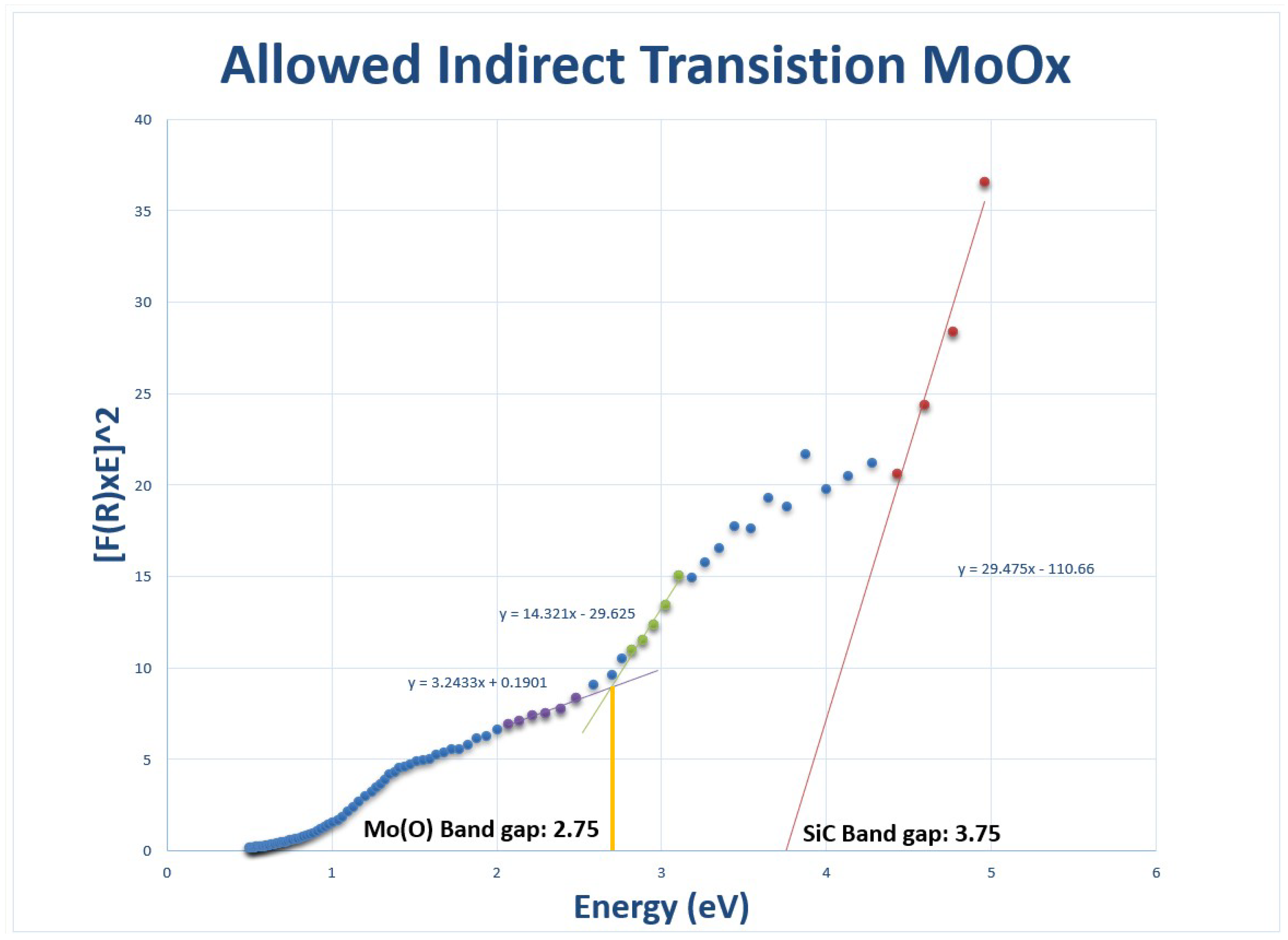
24]. Additionally, Mo oxide thin films that were prepared by electron beam evaporation and heated in the air exhibited an orthorhombic α -phase with an optical band gap of 3.2 eV [21,22].
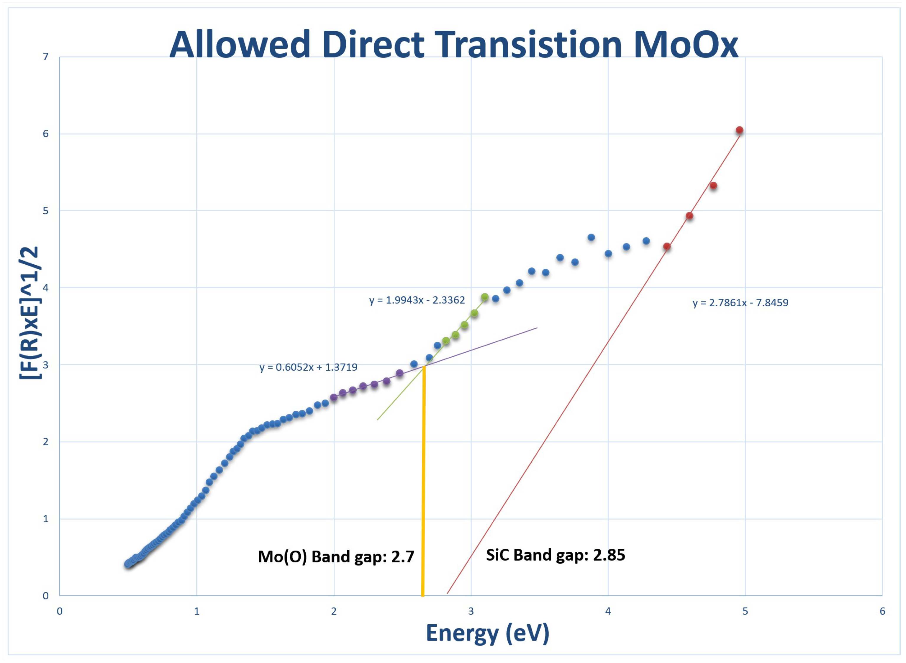
According to Dukstiene et al. [25], M o O 2 films exhibit a high Absorption Coefficient (k) for a direct band-to-band transition. The k is reported to be 1 × 10 4 1 cm , with an extinction of 2.1 times the refractive index as seen in Table 2. The band gap energy ranges from 2 to 2.4 eV and varies depending on the film thickness, density, and morphology. Rabalais et al. proposed a simple qualitative band model to account for the variability of the electrical and optical properties of M o O 3 x films as described in Equation (1) [26]. In this equation describing k as the extinction coefficient, α is the absorption coefficient and λ is the wavelength.
k = α λ 4 π
Assuming the bonding in the M o O 3 surface oxide is mostly ionic, the valence band orbital consists of electrons from the oxygen 2 p and the vacant 4 d and 5 s M o orbitals. In substoichiometric M o O x , an oxygen ion is electron deficient, resulting in defect orbitals that act as gap electronic states between the valence and conduction bands. These positively charged oxygen defects, which are not detected by positron spectroscopy, can increase carrier concentration. The M o 6 + sites can be reduced to M o 5 + with a 0.19 eV energy change, which moves an electron into the delocalized conduction band [27]. This process is responsible for the increased conductivity of M o oxide. While M o O 3 is a semiconductor with a band gap of 3.2 eV, when the oxide is reduced, its conductivity can increase by at least an order of magnitude by partial reduction to M o O x . Reduction produces shallow oxygen vacancies which transfer electrons to M o 6 + ions, forming M o 5 + or M o 4 + holes in distorted lattice positions, yielding a lowered band gap. The band gap for M o O 2 is 1.8 eV, and the oxide band gap approaches zero for x = 2.6 , at which the oxide exhibits metal-like properties. The electrical and optical properties of the M o O x film depend on its thickness and the equilibrated redox activity.
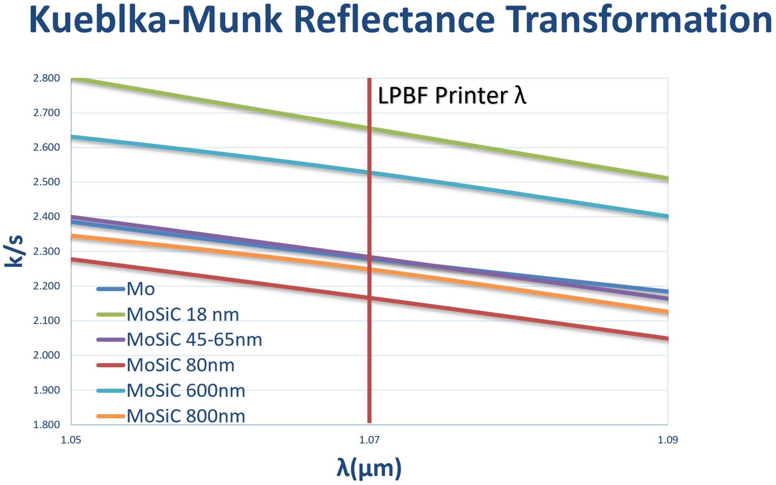
The minimum thickness required for the resonance condition of interference of light between the two interfaces of a M o O 3 coating on Mo at a wavelength of 1070 nm is 260 nm. When oxide coatings are applied on micron-sized Mo metal particles, resonance reflection coupling is expected to occur for the LB-PBF laser wavelength at thicknesses equal to small integer multiples of approximately 260 nm. Reflectance analysis is a useful tool to understand the behavior of such coatings. It has been observed in previous studies that the addition of small quantities of SiC particles can enhance the performance of LB-PBF parts under certain operational conditions. The presence of SiC may also increase the absorption of laser energy for laser powder-bed metal manufacturing by modifying melt pool dimensions and surface morphology [29].

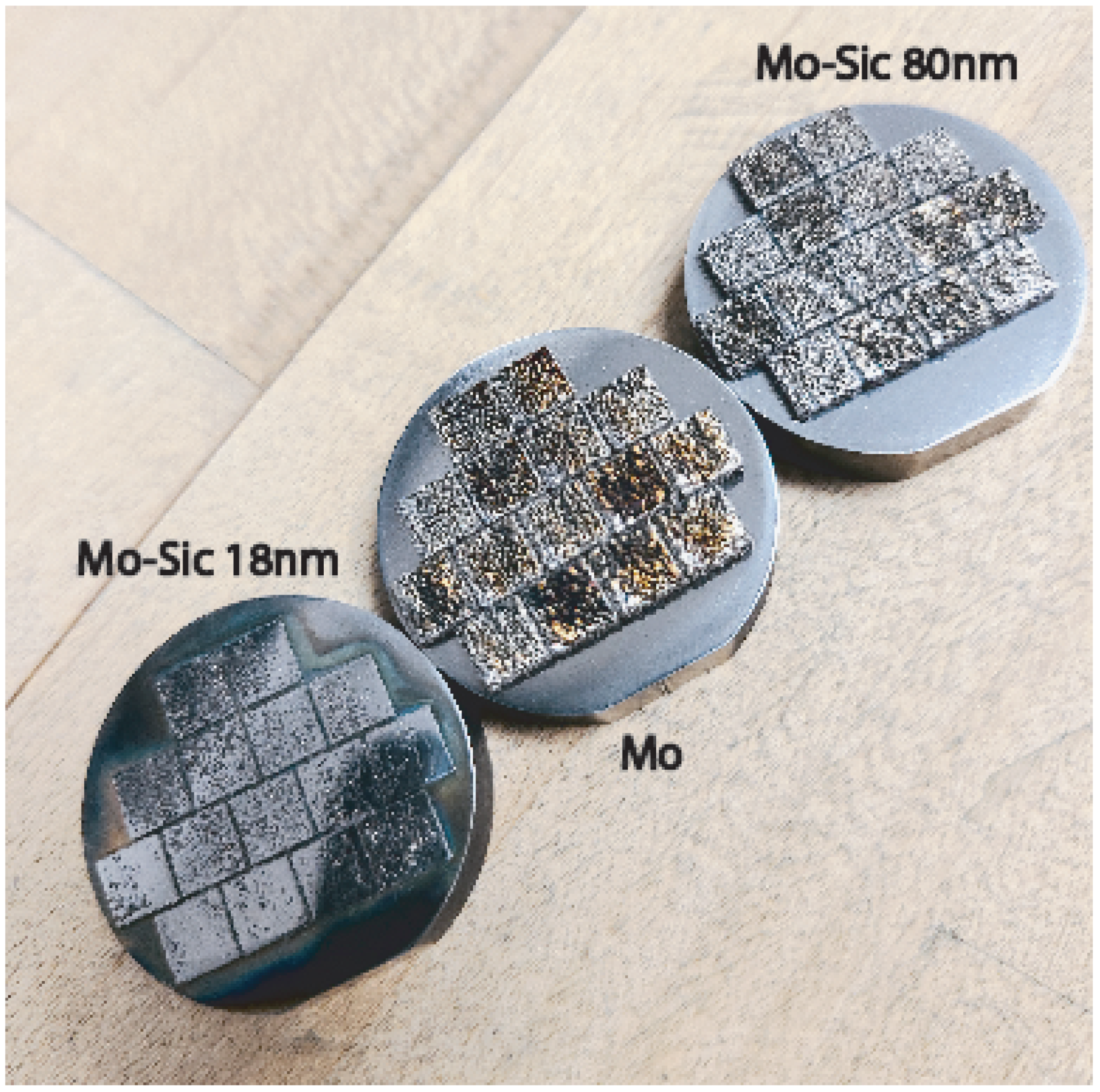
2.2. Van der Pauw Resistivity

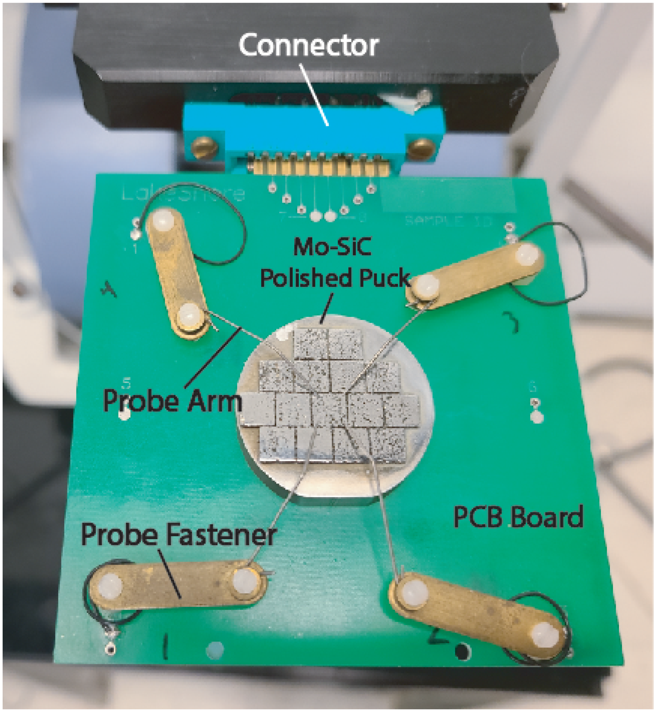
The Van der Pauw method is one of the most effective and widely used four-probe methods of measuring resistivity in thin film materials [30]. Some experimental setups can be indirectly measured using a non-contact eddy-current-based testing device. A schematic of the four-probe experimental setup for a square geometry can be seen in Figure 1. The Van der Pauw technique derives sheet resistance across a Two-Dimensional (2D) area. Sheet resistance normalizes a material’s resistance, making it invariant to scaling. Therefore, sheet resistance can be used to compare the electrical properties of materials with different compositions or sizes. The equation for sheet resistance is shown in Equation (2).
R s = π ( R + R ) 4 ln 2 f ( R R )
R R R + R = f R R cosh exp ln 2 f R R
R = V C D I A B
R = V D A I B C
Linear point-to-point resistance, which is variable to scaling, must be used to measure sheet resistance. As shown, Equation (2) depends upon paired probe arm contacts in the four-terminal contact array. R and R are shown in Equations (4) and (5) to be dependent on Voltage (V) and Current (I) between probes, where the subscripts indicate probe contact pairs. These referenced probe positions are shown in Figure 1.
Resistance measurements are intrinsically geometry-dependent and sensitive to the boundary and surficial conditions. Consequently, correction factors for fitting data to models are empirically derived and indicated by the function R R . These correction factors have been determined for a multitude of complex probe geometries, and the general equation is shown in Equation (3). In this equation, the ratio of R to R is dependent on relative probe positioning or probe position outline. In the case of a perfect square probe array, the left-hand side of Equation (3) reduces to two, which correspondingly makes the function one. Luckily, this probe setup is common and a correction factor of one is widely used across experiments [30,31].

2.3. Kubelka-Munk Model

Light interactions can be described in simplified terms using three wavelength-dependent mechanisms [32]. Firstly, the transmission of light through a guidance structure like optical fibers or light-shaping lenses [32]. Then the mechanism of either absorption, reflectance, or transmittance occurs. In the process of absorption, photons transfer all of their kinetic energy to electrons within the material and thus are converted into phonons [32]. The result is the heating of the matter. The process of transmission and reflection occurs at interfaces, where a light ray either penetrates the material or scatters off particles, atoms, or nuclei. These three mechanisms are strongly dependent on the wavelength of the electromagnetic radiation [32].
According to the Kubelka-Munk theory of diffuse reflectance, the energy of incident light in each layer of material can be expressed as E = R + A + T , where R denotes macroscopic reflectance, A denotes absorption, and T denotes transmittance. By integrating this formula over a semi-infinite opaque sample, Equation (6) can be derived. Rearranging this equation leads to Equation (7), which shows the ratio between total absorption and total incident light energy for opaque materials. Since there is no transmittance of light in opaque materials, the ratios of A T o t a l E T o t a l and R T o t a l E T o t a l are equivalent to A and R, respectively.
E T o t a l = R T o t a l + A T o t a l
A T o t a l E T o t a l = 1 R T o t a l E T o t a l = E = 1 R
The extinction coefficient of solid materials can be expressed as the sum of the k and the Scattering Coefficient (s), i.e., E = k + s . In the K-M, an increase in the s is associated with a decrease in particle size and results in an increase in reflectance. While for particle sizes below 1 μ m, the s-parameter decreases in proportion to the inverse of the scattering length, 1 d , as noted in Dai et al. [33] for larger mixed particle sizes the s-parameter is approximately constant and for large k/s, the ratio is proportional to absorbance. On the other hand, as a light ray encounters more scattering interfaces, the gls s increases, leading to a reduction in the penetration depth of radiation [33]. This reduction in penetration depth, combined with a decrease in particle size, causes an increase in the fraction of diffusely reflected light and a decrease in the absorbed fraction of radiation. Meanwhile, the average depth of penetration decreases with an increase in the k.
The representative layer theory is employed for mixtures of particles of different sizes. Dahm et al. demonstrated that the contribution of a particle type to absorption is proportional to its volume fraction, while its contribution to reflectance is proportional to the fraction of the cross-sectional area in the layer [34]. Thus, the mass fraction determines the contribution of a particle type to light absorption.
The efficiency of LB-PBF processes is largely determined by the ratio of absorbance to reflectance, which depends on the optimal wavelength range for a material. Surface-to-volume ratios, packing structure, oxidation level, and particle size distribution affect the interaction volumes and thus influence the optimal wavelength range [35]. This ratio plays a crucial role in optimizing LB-PBF systems and increasing part production efficiency [32]. Therefore, several models, such as the K-M model, have been developed to accurately predict and describe this ratio.
The K-M model is used to describe how light interactions differ between homogeneous and heterogeneous powder mixtures, with a focus on differences in diffuse reflectance. Diffuse reflectance was first developed to analyze powders under standard temperature and pressure conditions [36]. The propagation of light can vary significantly between homogeneous and heterogeneous media due to scattering off points in its path [36]. The K-M is widely used to describe diffuse reflection due to its simplifying assumptions in semi-infinite samples [36]. In the K-M model, all geometric details of a heterogeneous sample are summarized in a single parameter known as the s [36]. The s was introduced to account for internal scattering processes and is a semi-empirical parameter that depends mainly on the particle size and refractive index of the sample [36]. Unlike the k, the s is weakly dependent on wavelength and treated as a constant for a given sample, but it does change significantly with packing density [36]. The diffuse reflectance R i n f is given by Equation (8), where the k is shown in Equation (9), and it depends on the incident light wavelength λ and an arbitrary fitting coefficient κ that is usually taken to be 1 [37]. The K-M transformation, as shown in Equation (10), expresses the proportion between absorption concentration and scattering concentration about a unit volume of powder. Many researchers focus on accurately describing and predicting this proportion because it is crucial for optimizing LB-PBF systems and increasing part production efficiency [32].
Since log R i n f = log k log s , this gives the absorption spectrum offset by a scattering term displaced by log s . While the s might change with particle size, the absorption, A, for near-infrared diffuse reflectance is given by Equation (11).
R inf = 1 + k s k s ( 2 + k s )
k = 4 π λ
k s = ( 1 R inf ) 2 2 R inf
A = log ( 1 + k s k s 2 + 2 k s )
The K-M transform of the measured spectroscopic reflectance is proportional to the k and hence is proportional to the concentration [36]. Due to its simplicity, it has been widely used for diffuse reflectance transforms in standard infrared spectroscopy software of commercial Fourier Transform - Infrared (FT-IR) spectrometers. This model shows that smaller and heterogeneous mixtures will lead to greater absorption. Agreement with spectroscopy studies gives credence to applying the K-M model to oxidized metal powder mixtures.
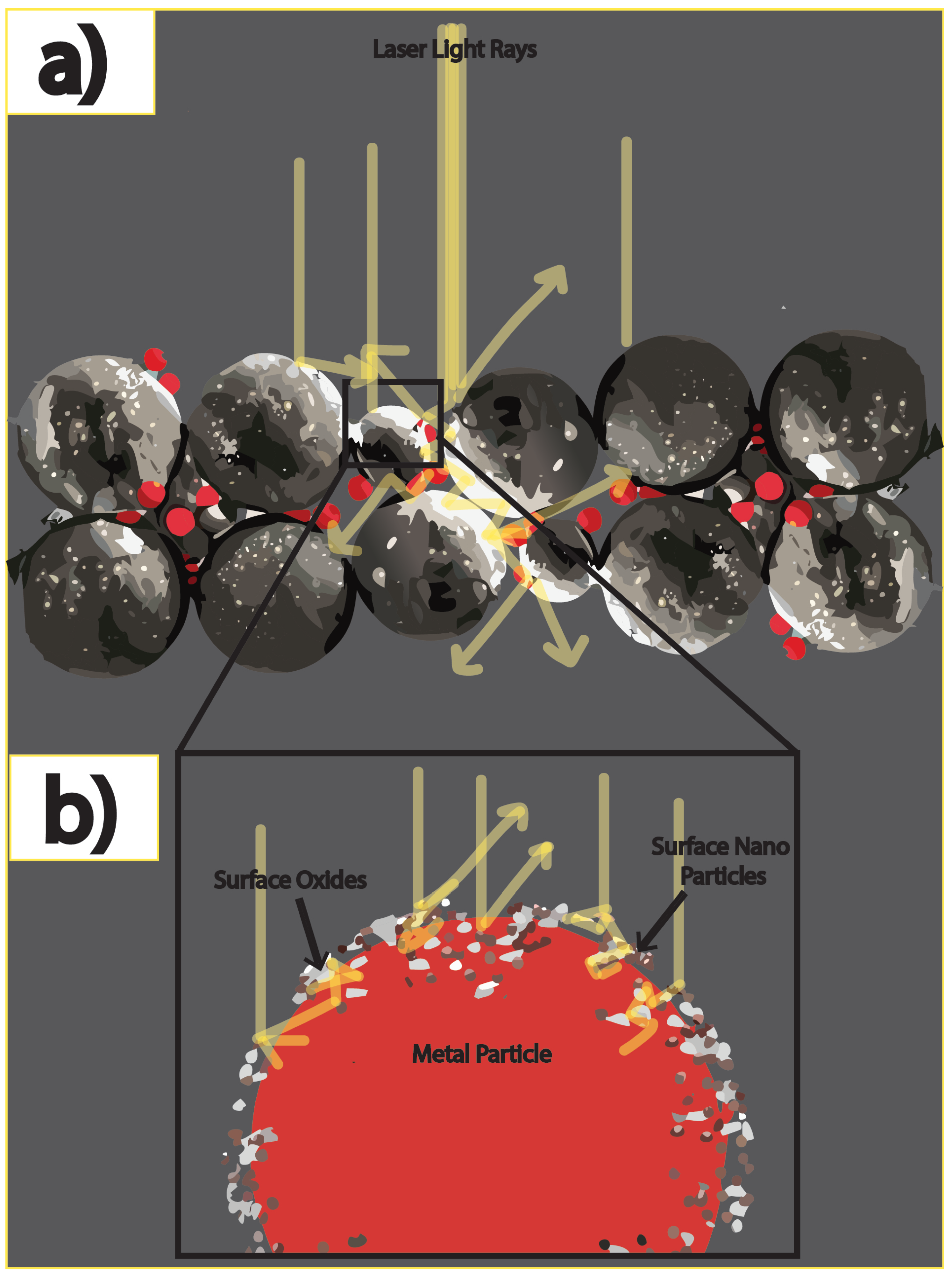
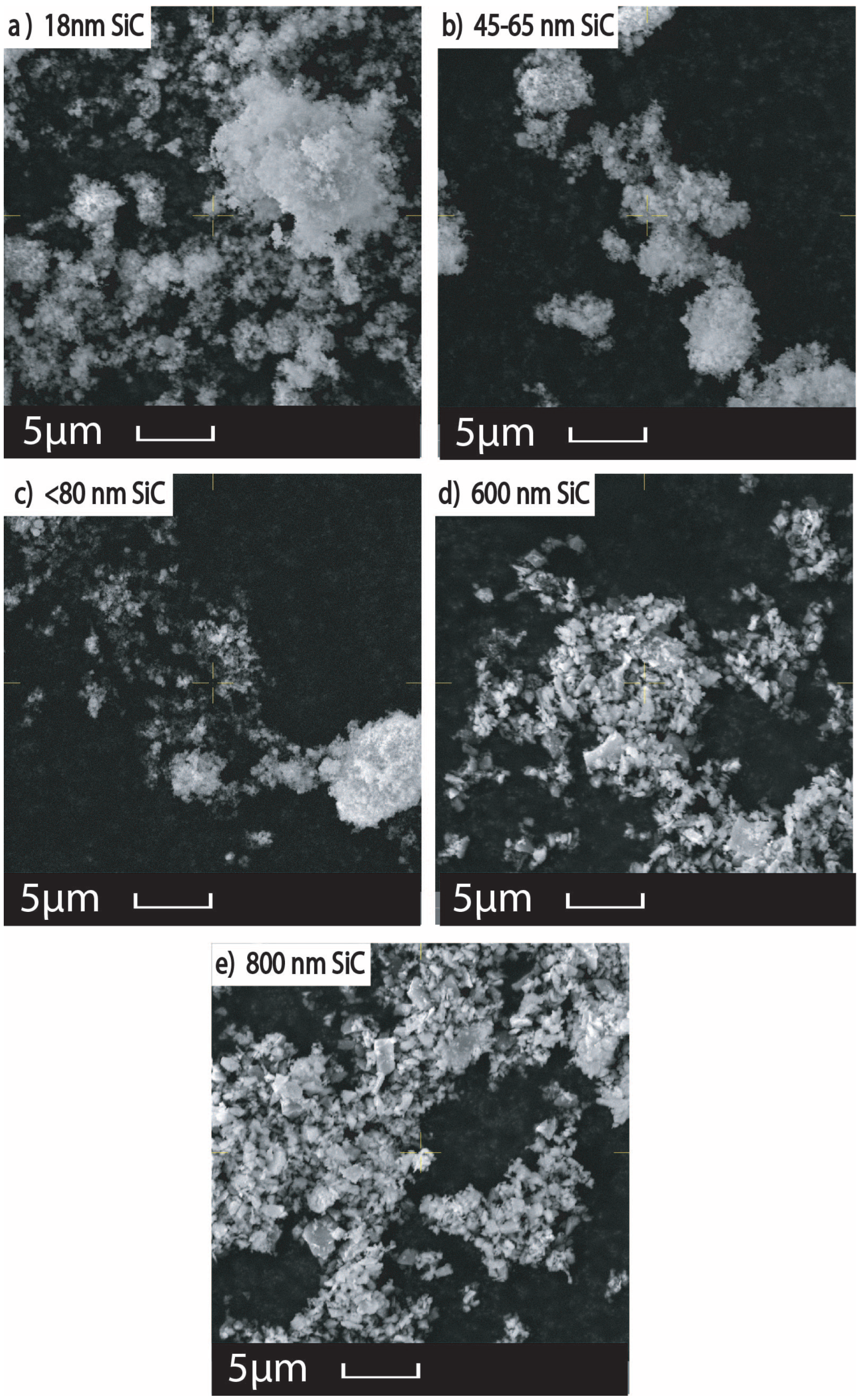
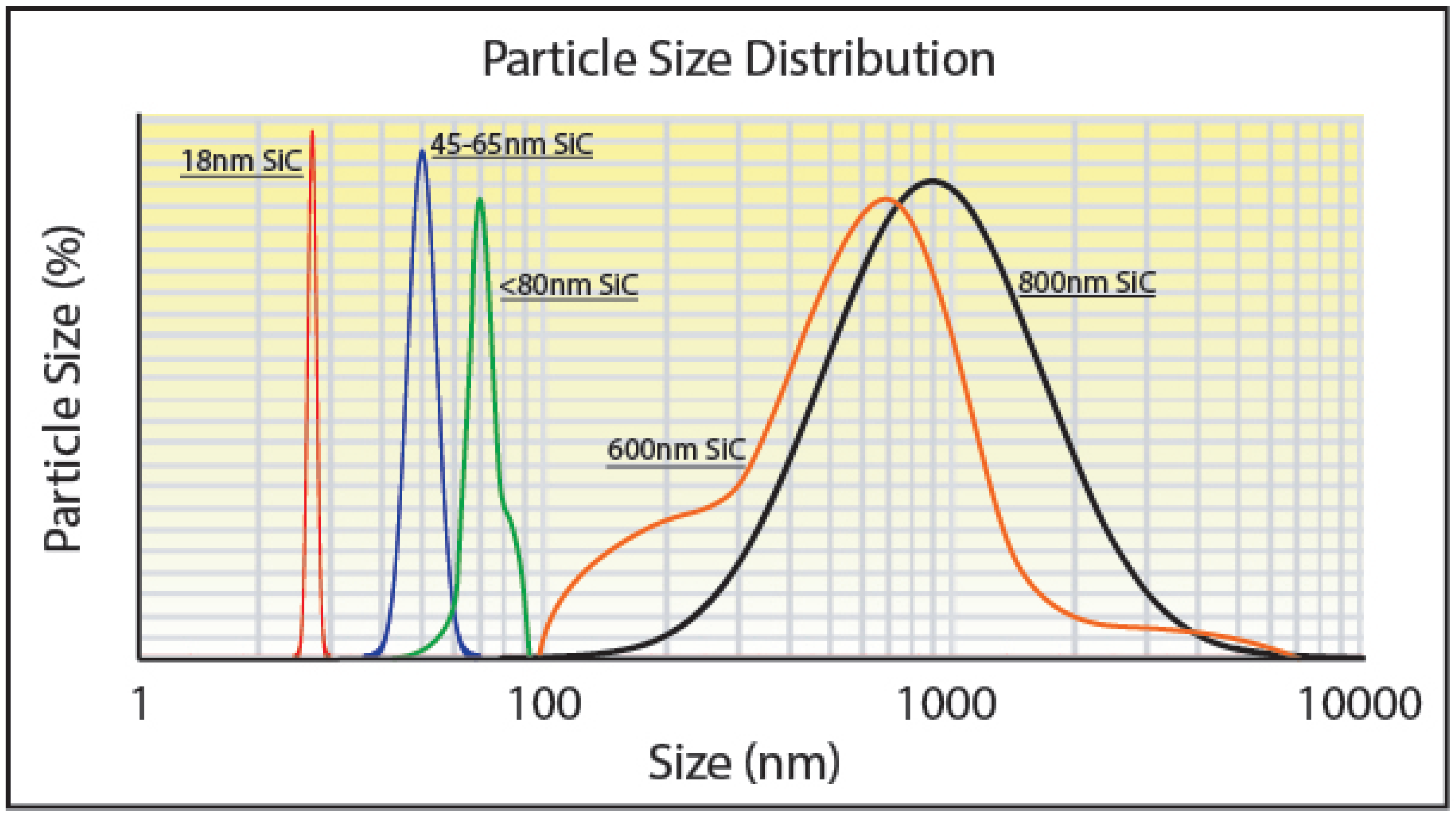
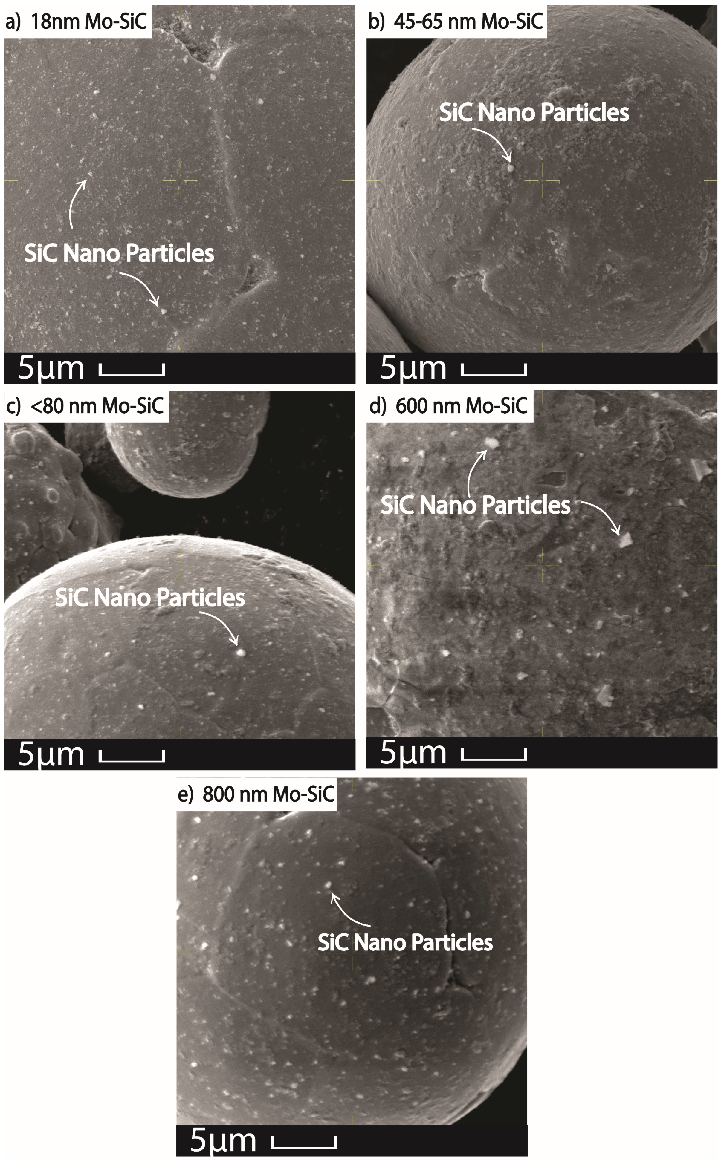
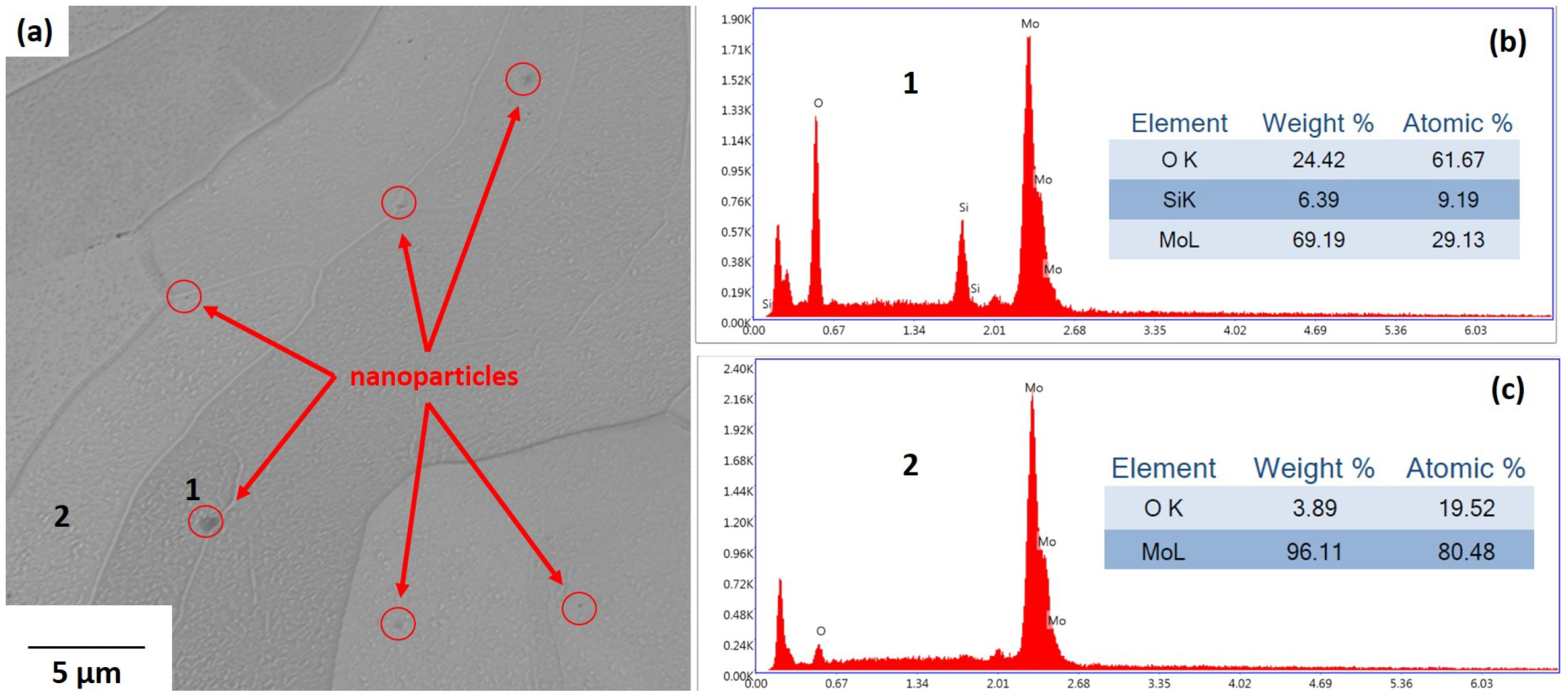
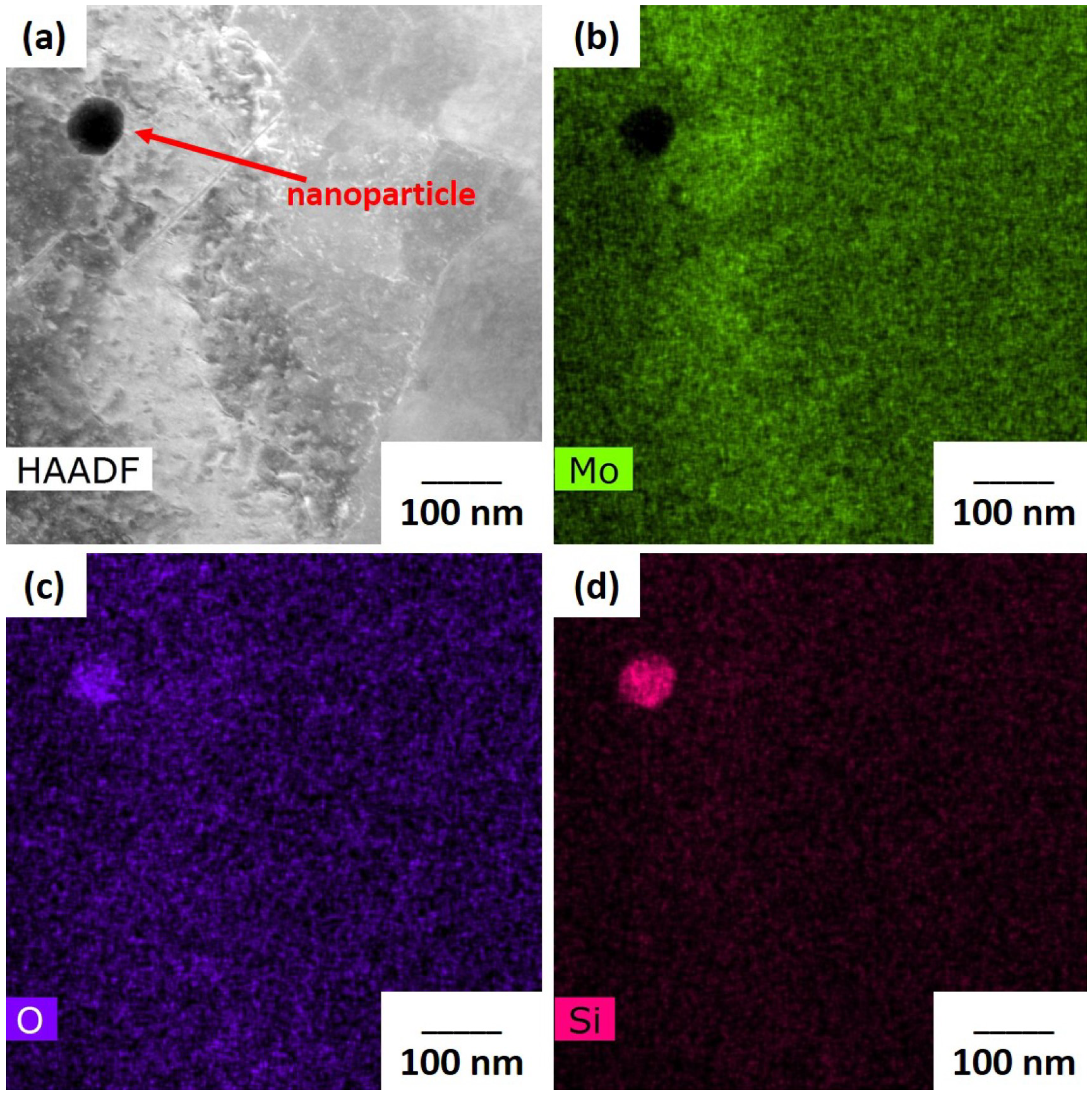
The addition of nanoparticles can increase the reflectivity via scattering as shown in Figure 2. The scattering cross section is proportional to the 6th power of the particle radius, producing scattering angles that increase with decreasing particle size. Enhanced scattering from smaller nanoparticles adsorbed on the oxide surface of the Mo particles enhances local light absorption in the M o O x layer approximately in proportion with the inverse of the nanoparticle radius. A study investigated light absorbance in more than 35 metal powders utilized for LB-PBF processes, where laser wavelengths ranging between 330 and 1560 nm were employed [32]. The powders displayed variations in grain size and degree of oxidation or degradation. The results showed that shorter wavelengths led to greater absorption across all powders. Furthermore, finer-grained powders exhibited higher absorption compared to coarse-grained and heavily oxidized powders, with a 2.4 to 3.3 times higher absorption factor across multiple wavelengths [32]. The researchers explained that the probability of multiple reflections increased for particles smaller than the diameter of the incident beam, leading to an increase in absorbance. This conclusion is supported by single ray tracing experimental models conducted on homogeneous A l S i 12 by Yang et al. [12]. The models demonstrated that if the particle size distribution was within the range of incident light wavelength, then the probability of multiple reflections decreased, resulting in Rayleigh and Mie scattering [12,32,37].
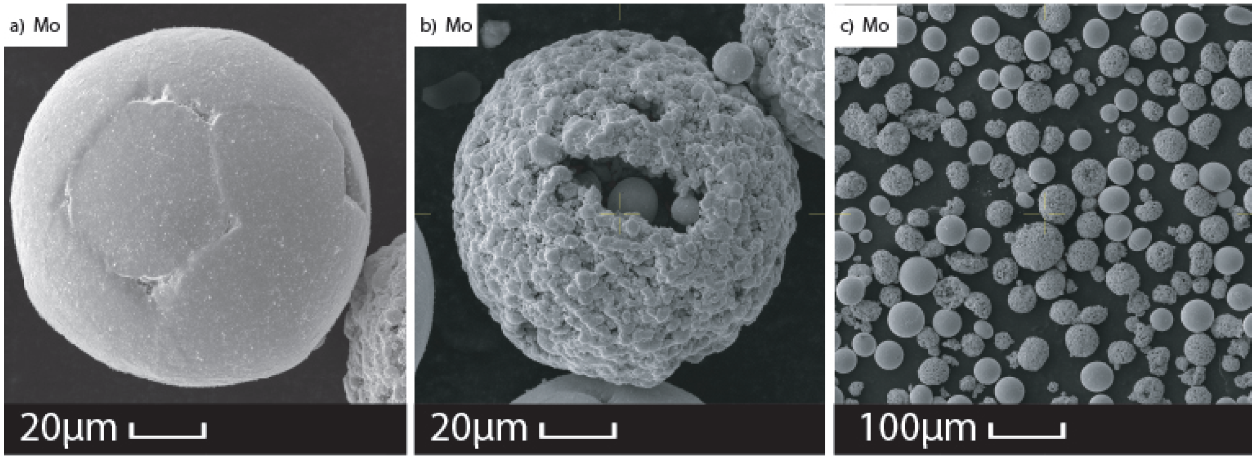
Consequently, these powder surfaces optically behaved as fully dense bulk material. The study also found that the morphology of the powders could produce the same phenomenon of increased light scattering and absorption [32]. Non-spherical or conglomerate particles with rougher surfaces can increase the probability of multiple reflections by providing a greater surface-to-volume ratio.

3. Materials and Methods

3.1. Material

Pure Mo and Mo containing SiC specimens were produced for this study. Feedstock powders used for specimen production were 99.99% atomic Mo micropowder with a particle size of 45 ± 15 μ m and 99% atomic β SiC nanopowder with varying particle sizes shown in Table 3 and Table 4 provided by Tekna (Sherbrooke, QC, Canada) and US Research Nanomaterials, Inc. (Houston, TX, USA) respectively.
The Mo micropowder had both spherical and pseudo-spherical particles as shown in Figure 3. These pseudo-spherical particles were shown to have high porosity. The poor atomization was thought to result from low-heat sintering, where the plasma chamber failed to maintain high enough temperatures for proper spherialization. However, this powder was used consistently across all prints and thus was a control during experimentation. Figure 3 shows the various morphologies of this feedstock powder and the size distributions indicated in Table 3. The pseudo-spherical particles account for 45 % ± 5 % of the population and are generally seen to occur in larger particle sizes [38].
The SiC nanopowder, shown in Figure 4, ranged from 18 to 800 nm in average particle diameter. These small and highly densified powders possessed high purity, narrow range particle size distribution, and larger specific surface area. The SiC nanoparticles used were reported to have higher chemical stability, thermal conductivity, lower thermal expansion coefficients, and better abrasion resistance than the Mo micropowder [39]. The SiC microhardness was reported to be 2840 to 3320 kg mm 2 or 9.5 Mohs, which puts it between corundum and diamond on the Mohs Hardness Scale [39,40]. However, its mechanical strength is reportedly higher than that of corundum with a compressibility coefficient 0.21 × 10 6 and density of 3.216 g cm 3 at 288 K [40]. Its decomposition temperature was reported to be 2973 K with a thermal expansion coefficient of 2.98 × 10 6 at 1173 K [39]. The nanoparticle SiC is reportedly sold for many AM processes related to ceramics and semiconductors due to its excellent thermal and electrical conductivity and resistance to oxidation at high temperatures [40]. All nanoparticle SiC contained elemental impurities, including free Si and C, due to processing techniques. These synthesis processes are listed in Table 4, which also contains the bulk density of unpacked SiC powders. Figure 5 more accurately shows size distribution data provided by US Research Nanomaterials, Inc. (Houston, TX, USA). These SiC nanoparticles were sourced differently from the SiC particles used in previous studies [4,5], which had an average size of approximately 200 nm and were stored in laboratory.
Table 3. Typical Properties of Mo powder feedstock (Product number: 25563) [38].
Particle Size Distribution
Size ( μ m) +45Typical Results: <2%  Max: 5%
Size ( μ m) −45Typical Results: >98%  Min: 95%
Laser scattering (Microtrac) D10Typical Results: >20 μ m  Min: 15 μ m
Chemistry
Molybdenum>99.9% (m.b.)
Oxygen<250ppm
Density
Tap Density>5 g/cm3
Morphology
Spherical DegreeTypical Results: >95%  Min: 90%
Table 4. SiC Powder Properties and Synthesis Methods (US Research Nanomaterials [39]).
ParticleCompositionSynthesis
Size Purity SiO2% Si% C% Al% Fe% Ca% Density (g/mL) Method
18 nm0.99+ 3 × 10 4 0.00180.00490.03Laser
45–65 nm0.99+0.00240.00760.05Plasma CVD
<80 nm0.99+0.00240.00760.05Plasma CVD
600 nm0.99+<0.0050.020.060.050.09Plasma Atom.
800 nm0.99+<0.0050.020.060.050.09Plasma Atom.
In Table 4, it can be observed that the initial SiC particles contain more C than Si. Thus, it is assumed that the prepared environment is likely to be rich in C. Based on this, it is expected that the concentration of Si vacancies in the material will be higher than that of C vacancies. These interstitial defects in SiC can have a significant impact on the material’s electronic and mechanical properties.

3.2. Powder Mixing

The various SiC particles and Mo particles were combined into a powder mixture with a weight proportion of 0.01 to 99.99, respectively. The resulting Mo-0.1SiC mixtures were used for all experimental tests and prints. These Mo-0.1SiC mixtures were made using a FlakTec Inc. DAC 250.1 FVZ-K SpeedMixer (Landrum, SC, USA). Powder mixture batches were made in 200 g quantities in a 250 mL cylindrical plastic cup with a threaded lid.
The prepared cups were then clamped to an oscillating arm on the FlakTec SpeedMixer for 5 min at 1500 Hz. Following mixing, the powders were tested with a humidity probe and found to have levels below 0.05 % water content. Metallic dopping sticks coated with conductive and adhesive C tape were also plunged into the powder mixtures to collect thin powder coating samples for SEM and Energy Dispersion Spectroscopy (EDS) analysis. SEM images of these powders, shown in Figure 6, were taken using a MIRA-3 field emission scanning electron microscope (TESCAN, Brno, Czech Republic). These images were then analyzed via EDS using an EDAX TEAM Pegasus system (Ametek Materials Analysis Division, Mahwah, NJ, USA). Figure 6 shows a uniform coating of SiC nanoparticles on the Mo microparticles.

3.3. Reflectance Spectroscopy

Reflectance measurements for wavelength ranges between 250 and 2500 nm in 10 nm increments were conducted by AZ Technologies LLC (Huntsville, AL, USA). In preparation for powder shipment, 4 mm deep Poly Lactic Acid (PLA) dishes were printed out with an Ultimaker 2+ Connect Printer (Utrecht, The Netherlands). The mixed powders were then placed in the printed dishes, capped with a 2 mm Potassium-Bromide (KBr) window, and sealed with super glue as seen in Figure 7. The optically clear KBr windows sat on an internal ledge of the dish and were chosen to encapsulate the powders due to their consistent absorption spectra across the measured range of wavelengths. The prepared powder samples were measured by the solar reflectance of materials using the integrating spheres technique by the ASTM standard method E 903-12. The measurements were run on an AZ Tech TEMP 2000A (Huntsville, AL, USA) with an absolute integrating sphere geometry and a light beam angle of 15 ° from horizontal. The uncertainty for these measurements is shown in Table 5. Three wavelength sweeps were conducted on each sample, and reflectance was reported as an absolute fractional value to 3 decimal points. The results of this reflectance data, as discussed in Section 3.3, surmounted in the truncation of tested powder mixtures to pure Mo, Mo-0.1SiC with 18 nm SiC, and Mo-0.1SiC with 80 nm SiC.
Table 5. Measurement Statistics of uncertainty where gray bodies refer to flat uniform surfaces with monotonic reflectance and non-gray bodies refer to background surfaces with variability in reflectance [41].
Uncertainty:±0.01 of a full-scale value of 1.0 (gray bodies)
±0.03 of a full-scale value of 1.0 (nongray bodies)
Repeatability:±0.007 of a full-scale value of 1.0

3.4. Pad Production

Pads were consolidated on polished 32 mm Mo puck substrates using a GE Concept Laser M2 Cusing Direct Metal Laser Sintering machine (Boston, MA, USA) with a 400 W continuous wave single mode Ytterbium (Yb) fiber laser [42]. Compressed nitrogen was used as a shielding gas to maintain oxygen levels within the print chamber at or below 1000 Parts Per Million (ppm) as monitored by the built-in printer oxygen sensor system controls. This threshold was the lowest detectable level for the system, and the nitrogen gas was pressurized to 20 millibars with a flow rate of 5 m s into the chamber. Pucks were polished to obtain optimal printing conditions for powder consolidation and adhesion to the substrate. Using a fixed hatch spacing of 50 μ m and a layer thickness of 40 μ m, laser power, speed were varied for each square pad. The pads were printed with a meander laser scan pattern that had 90° rotations between layers. The printed cuboid pads had final dimensions of 5 mm × 5 mm × 2 mm. These printed pads can be seen in Figure 8. The printing parameter template for each printed puck can be seen in Figure 9.

3.5. Optical Porosity

After taking SEM images, the pads were polished. The pads were mechanically ground to 800 grit with SiC grinding paper using an EcoMet Beuhler 300 grinding and polishing machine (Lake Bluff, IL, USA). This was done to prepare the cuboid pads such that the internal pores could be observed through optical microscopy. Once the oxide layer was removed and geometry flattened, Optically Determined Density (ODD) measurements were conducted.
Four independent images at 20× were taken of every polished cuboid pad on each puck. This was done to fully encapsulate the porosity of each specimen, as pore size and distribution varied across the pad. The taken images were then fed into a MATLAB 9.6 image analyzer package (Natick, MA, USA), converted to grey-scale, and ultimately turned into a binary black-and-white image based upon a threshold value.
Pixels below the threshold value were taken as true and depicted as white. Correspondingly, false pixels with grey-scale values above the threshold are depicted as black. Keeping this in mind, low counts of true pixel numbers are ideal for forming good binary images. The sum of true pixel values, obtained at this threshold value, was then used to calculate ODD as shown in Equation (12).
O D D = T r u e P i x e s l s T o t a l P i x e l s 100

3.6. Van der Pauw Resistivity

Measurements for sheet resistivity were taken on a Lake Shore Warehouse Hall Effect Measurement Systems (Westerville, OH, USA). The experimental setup consisted of a horizontally oriented Printed Computer Board (PCB) mount with four swivel probe arms. The puck of polished specimens was placed in the center of this board. The probe arms were then manually placed and tensioned on the corners of each polished cuboid specimen. This described setup can be seen in Figure 10.
The placed probes were numbered from 1 to 4 in counterclockwise order as shown in Figure 10. An I-V curve was then obtained from each set of adjacent probe pairs for a total of four I-V curves per cuboid specimen. In each I-V curve, I was increased from 100 μ A to 1 mA by a step size of 100 μ A for a total of ten data points. Each data set was recorded as a text file Comma Separated Value (CSV) and fed into a MATLAB script (Natick, MA, USA) to calculate sheet resistance using the formulas described in Section 2.2.

4. Results

4.1. Surface Resistivity and Defect Characterization

Sheet resistance measurements conducted on printed pads revealed strong correlations between processing parameters and defect structures. As shown in Figure 11, all sample sets exhibited inverse relations between sheet resistance and LED, with Mo-0.1SiC containing 80 nm SiC particles showing significantly reduced sheet resistance values. The linear correlations exceeded 0.9, indicating a robust relationship between processing conditions and electrical properties. The relationship between processing parameters and electrical properties was analyzed using multiple linear regression. LED values showed a strong negative correlation with sheet resistance (R2 = 0.92, p < 0.001), while particle size effects were most pronounced in the 80 nm samples (mean difference = 6.2%, 95% CI [5.1%, 7.3%]).
Consolidation improved with LED for all samples. Cracking appeared for high-power, high LED prints. Figure 11 shows that, while resistivity metric of nano-heterogeneity decreased in the presence of more scattering nanoparticles, nano-heterogeneity shows no enhancement for LB-PBF of Mo or for Mo- 0.1 SiC with 18 nm SiC particles and was independent of LED.
PALS analysis provides direct evidence linking these resistivity measurements to specific defect types. In Mo metal, distinct positron lifetime signatures correspond to different defect structures: 103 ps for un-defected Mo, 115 ps for polycrystalline regions, 135 ps for extended dislocation defects, and 170 ps for monovacancy defects. Larger microvoid vacancies exhibit progressively longer lifetimes up to 430 ps. The intensity of these lifetime signatures varies systematically with LED, demonstrating a direct correlation between processing parameters and defect formation. While positron spectroscopy is insensitive to the holes that oxygen vacancies can form, it is sensitive to the nano pores that can be formed by clustering of mobile nanovacancies [43].
The relationship between sheet resistance and defect structure manifests through two primary mechanisms. First, microporosity creates physical barriers to electron transport, forcing more circuitous conduction paths. Second, nanodefects—including dislocations, vacancies, and impurities—act as electron scattering sites. This scattering effect becomes particularly pronounced as defect sizes approach nanoscale dimensions, a leading to significant variations in local electrical properties. The distinct behavior observed in Mo-0.1SiC with 80 nm particles is of particular significance. The change in resistivity slope suggests a fundamental shift in electron transport mechanisms, correlating with PALS data showing modified defect distributions. The larger SiC particles experience slower oxidation kinetics than 18 nm particles, altering the formation of oxide-mediated defect structures. This size-dependent behavior appears in resistivity measurements and positron lifetime distributions, providing complementary evidence for the proposed defect-mediated conduction mechanism. Statistical analysis confirms the significance of these observations. Student’s t-tests (Table 6) demonstrate that Mo-0.1SiC with 80 nm SiC exhibits statistically distinct resistivity characteristics (p < 0.025). This distinction aligns with PALS measurements showing unique defect distributions in these samples, particularly in the relative intensities of different lifetime components.

4.2. Electronic Structure and Defect States

The relationship between defect structures and electrical properties can be understood through band gap analysis of the constituent phases. Our optical measurements reveal a complex interplay between M o O x surface layers and SiC particles, with both contributing to the overall electronic structure through distinct mechanisms.
α - M o O 3 is an n-type semiconductor with an indirect bandgap of 3.2 eV and a direct bandgap of 2.3 eV. The primary electron transfer pathways occur through the M o O x oxide semiconductor layer on Mo particles with allowed direct and indirect of 2.7 eV in Figure 12 and 2.75 eV in Figure 13. Our values of bandgap for samples containing Mo powder coated by oxide, obtained through Kubelka-Munk-Tauc (K-M-T) Model Model analysis, are shown to be the same. These agree with other reported M o O x band gaps of 2.3 2.8 eV [9,44], Reports of smaller bandgap measurements for M o O x are due to partial reduction of M o O 3 to M o O x ( x < 3 ) , forming oxygen vacancies. [45] The K-M-T plots show that β SiC in the Mo-0.1SiC mixtures exhibits higher band gaps of 2.85 eV (direct) and 3.75 eV (indirect), consistent with literature values of 2.4 3.8 eV [46,47].
Of particular significance are the narrow absorption lines associated with defects in SiC, which appear near the 1.08-micron laser wavelength used in LB-PBF processing. Our measurements identified weak absorption features at:
  • 18 nm particles: 1.1 eV, 1.4 eV, and 1.5 eV
  • 55 nm particles: 1.1 eV, 1.2 eV, 1.3 eV, and 1.4 eV
  • 80 nm particles: 1.1 eV, 1.4 eV, and 1.5 eV
These absorption features correspond to silicon vacancy defects (VSi) in different crystallographic sites, as confirmed by quantum calculations [48]. The presence and intensity of these defect states correlate directly with the observed resistivity trends. Specifically, the 80 nm SiC samples, which showed the lowest sheet resistance, exhibited distinct absorption patterns indicative of modified defect distributions.
The reflectance spectra shown in Figure 14 are dominated by broad oxide absorption Mo below the knee, which is just below the laser wavelength used for LB-PBF processing. The hints of structure below 1.75 nm evidence defects in the amorphous Mo oxide layer. The correlation between defect-related absorption and electrical properties becomes particularly evident when examining the wavelength-dependent extinction coefficient ( E = k + s ). Although the M o O x absorption (k) remains constant across each of the samples, the total extinction increases with decreasing particle size mainly due to enhanced scattering (s). This relationship manifested in the reflectance measurements in Figure 14 may ultimately influence the formation of the defect during processing LB-PBF. This is further shown in the discrepancy in the size distribution shown in Figure 15.
The Saunderson correction for measured reflectance, given by Equation (13), provides additional insight into the role of surface oxides:
R c = R m k 1 1 k 1 k 2 ( 1 R m )
where differences in the refractive index (2.4 for M o O 3 versus 2.6 for SiC) result in distinct surface optical properties. These variations influence both energy absorption during processing and the resulting defect structures, as evidenced by both PALS and resistivity measurements.

4.3. Nanoparticle Chemical Analysis

Comprehensive chemical analysis was conducted to investigate the distribution and composition of nanoparticles within the Mo-0.1SiC matrix. High-resolution SEM imaging coupled with EDS point analysis revealed critical insights into the oxygen scavenging mechanism and secondary phase formation. Figure 16 shows the detailed characterization of nanoparticle inclusions, where point EDS analysis demonstrated distinct compositional differences between the nanoparticles and bulk matrix.
The point analysis, shown in Figure 16b, revealed that the nanoparticles contained significant concentrations of Si and O, while the bulk material Figure 16c showed predominantly Mo content. This spatial segregation of elements provides direct evidence for the proposed oxygen scavenging mechanism, where SiC nanoparticles preferentially react with oxygen to form silicon oxide compounds.
To further elucidate the spatial distribution and chemical state of these nanoparticles, Tunneling Electron Microscopy (TEM)-based EDS mapping was performed, as shown in Figure 17. The High-angle Angular Dark Field (HAADF) imaging (Figure 17a) revealed distinct contrast variations corresponding to compositional differences, while the elemental mapping Figure 17b–d provided a detailed spatial distribution of Mo, O and Si. Notably, the EDS maps confirmed the formation of oxygen-rich regions coinciding with Si concentrations, while showing the depletion of Mo in these areas. The absence of detectable C signals above background levels in or around the nanoparticles suggests a complete reaction of the original SiC particles during processing.
These analytical results provide quantitative support for the oxygen scavenging mechanism proposed earlier, demonstrating that SiC nanoparticles actively participate in oxygen scavenging during the LB-PBF process. The uniform distribution of these oxide-rich nanoparticles throughout the matrix, coupled with their distinct chemical composition, suggests a controlled reaction process that contributes to the enhanced electrical properties observed in Section 4.1.
The measurement of electrical conductivity reveals microcrystalline molybdenum with interspersed nanometer-sized regions of molybdenum oxide as shown in Figure 17c. The conduction through this matrix of molybdenum metal and metal oxide is not simply a matrix of conductor and insulator, as the oxide itself contributes to conductivity. Defected molybdenum oxide behaves as an extrinsic conductor with conductivity arising from defect charge carriers in the crystalline material. For M o O x species, conductivity improves as the M o / O = x ratio increases, with the oxide exhibiting good metal-like conduction properties for x = 2 in M o O 2 [49].
The activation energy for conduction is typically 0.05 eV. Conduction through the molybdenum oxide regions increases when equilibrated with sufficient oxygen vacancies (represented by x in M o O x ). This defect-rich molybdenum trioxide has significantly higher electrical conductivity compared to pure M o O 3 due to the formation of free charge carriers from oxygen vacancies. When molybdenum oxide regions are more reduced, the conductivity is enhanced due to oxygen vacancies that act as electron donors. In this case, achieving equilibrium with mobile SiO and Carbon Monoxide (CO) in a nanoporous matrix will promote this reduction process and enhance conductivity. In general, conductivity in the M o O x portion of the matrix serves as a measure of vacancy defects in partially oxidized molybdenum [50,51,52].

4.4. Supporting Microstructural Evidence

The microstructural analysis provides corroborating evidence for the defect-mediated electrical behavior observed through resistivity and PALS measurements. Optical porosity measurements reveal a systematic relationship between processing parameters and defect formation, with LED values showing a clear inverse correlation to void formation. This lasing process difference corresponds to the printed surface morphology of each print shown in Figure 18, Figure 19, and Figure 20.
The relationship between defect structures and energy coupling efficiency can be understood through the K-M model. Smaller SiC particles increase the surface area per unit volume, enhancing powder surface roughness, which increases scattering events. This mechanism follows the theoretical prediction that increased scattering leads to higher absorption probability. The practical manifestation of this effect appears in weld bead characteristics, where enhanced energy coupling produces more uniform melting and allows sufficient time for gas evolution, thereby reducing both micro and nano-scale defects. This reduction in defects can be shown by the optical data of each material in Figure 21 and Figure 22.
Statistical significance testing (Table 7) confirms these observations, with Mo-0.1SiC containing 80 nm particles showing significantly different variances in both porosity and resistance measurements compared to other compositions. F-test results demonstrate at least one differing mean in each property measurement, with particular significance in the electrical properties (p < 0.025). The connection between microstructure and electrical properties becomes particularly evident when examining the role of oxygen. In LB-PBF processing, oxygen primarily exists at Mo particle surfaces, where it can react with Si, C, and mobile defects. The competition between surface oxidation and SiC reactions fundamentally influences defect mobility and annihilation. In pure Mo, surface oxygen creates a defect gradient that promotes annealing. However, in Mo-0.1SiC, the formation of CO and SiO modifies this mechanism, as evidenced by both microstructural observations and electrical measurements. This interplay between chemical reactions and defect formation manifests differently with varying SiC particle sizes. The 80 nm particles, due to their slower oxidation kinetics, promote more stable defect structures that enhance electrical conductivity. This size-dependent behavior appears consistently across multiple characterization techniques, providing robust support for the proposed relationship between processing conditions, defect formation, and electrical properties.

5. Conclusions

  • The addition of Silicon Carbide (SiC) nanoparticles altered absorption by the original powder mixture in a more complex manner than merely the order of increasing scattering with decreasing particle size. K-M electronic absorption analysis of reflectance spectra for powder mixtures revealed the interplay between absorption by M o O x surface layers ( E g = 2.7 2.75 eV) and SiC particles ( E g = 2.85 3.75 eV). In addition to the scattering influence of the SiC nanoparticles, the presence of silicon vacancy defects in SiC through absorption enhancement at 1.1 1.5 eV, creates additional electronic absorption resonant with the Ytterbium (Yb) fiber laser energy at 1.2 eV.
  • Added nanoparticles of SiC fundamentally alter the defect structure and the electrical conductivity properties of Laser Powder Bed Fusion (LB-PBF)-processed Molybdenum (Mo). Oxygen scavenging reactions of SiC forming mobile Carbon Monoxide (CO) and Silicon Monoxide (Silicon Monoxide (SiO)) were complete in the printed samples since carbon was absent and silicon was found largely as an oxide condensed into separated microparticles. Chemical analysis by X-Ray Photoelectron Spectroscopy (XPS) and Energy Dispersion Spectroscopy (EDS) confirmed the oxygen scavenging mechanism, revealing silicon oxide formation with characteristic binding energies at 103.5 eV (Si 2 p ) and 532.8 eV (O 1 s ). Oxygen was also distributed uniformly throughout the Mo matrix. Quantitative oxygen mapping showed a 37 ± 4 % reduction in bulk oxygen content compared to unmodified Mo. The processing-structure relationships demonstrated statistical significance ( p < 0.001 ) across all particle sizes, with optimal performance achieved at Linear Energy Densities (LED) values of 2.0 2.2 J/mm. This optimization window corresponds to measured melt pool temperatures of 2350 ± 75 °C, as determined through pyrometer measurements.
  • Positron Annihilation Lifetime Spectroscopy (PALS) analysis revealed distinct positron lifetime signatures corresponding to specific defect types in the Mo matrix (103–430 ps). The addition of SiC nanoparticles produced quantifiable improvements in electrical performance, with added 80 nm particles achieving a 6.2 ± 0.4 % reduction in sheet resistance at 2.0 J/mm LED ( p < 0.001 ). This size-dependent SiC nanoparticle reaction mechanism correlates directly with reduced porosity ( 46 ± 3 % decrease) and modified nano-defect distributions confirmed through PALS as well as resistivity measurements. This size-dependent behavior stems from different oxidation reaction kinetics of SiC on Mo oxide surface which reduces M o O 3 resulting in altered defect diffusion and enhanced electrical conductivity.
  • Structure measures of porosity and resistivity were improved with added SiC nanoparticles of all sizes. Processing-structure relationships show strong statistical significance, with LED directly influencing defect formation and distribution. High laser power combined with intermediate scan speeds produces improved microstructures, although the LED parameter alone insufficiently captures the complexity of defect evolution. Resistivity and microporosity changes varied over the largest range with power and scan speed for the Mo- 0.1 SiC samples by addition of 80 nm nanoparticles. These improvements were strongly correlated with LB-PBF parameters represented by L E D = P / v for samples having added 80 nm size SiC nanoparticles. The average correlation coefficients of porosity and resistivity with P / v 1 / 2 , approximately proportional to absorbed energy density, were comparable to the property correlations with LED. Only small property enhancements with LED were observed for particle sizes smaller than 80 nm, consistent with the hypothesis that for smaller SiC particle size, oxygen in the M o O x surface was depleted more rapidly at a lower temperature than the ultimate melt temperature. The mechanism of property enhancement involves multiple complementary processes: increased laser energy absorption (up to 3 % in near-infrared wavelengths), modified oxidation kinetics, and controlled defect formation. This synergistic behavior, particularly evident in the 80 nm SiC nanoparticle composition, suggests a pathway for further optimization of LB-PBF-processed refractory metals through control of particle size distributions and processing parameters.

Author Contributions

Project administration, A.M., L.B. and R.K.; conceptualization, A.M., N.E. and R.K.; methodology, A.M., N.E. and R.K.; investigation, A.M. and N.E.; writing—original draft preparation, A.M. and N.E.; writing—review and editing, A.M., N.E., R.K. and L.B.; supervision, L.B. and R.K. All authors have read and agreed to the published version of the manuscript.

Funding

This research received no external funding.

Institutional Review Board Statement

Not applicable.

Informed Consent Statement

Not applicable.

Data Availability Statement

The data presented in this study are available on request from the authors.

Conflicts of Interest

The authors declare no conflicts of interest.

References

  1. Sturm, D.; Heilmaier, M.; Schneibel, J.H.; Jéhanno, P.; Skrotzki, B.; Saage, H. The influence of silicon on the strength and fracture toughness of molybdenum. Mater. Sci. Eng. A 2007, 463, 107–114, TMS 2006, Mukherjee Symposium. [Google Scholar] [CrossRef]
  2. Li, N.; Huang, S.; Zhang, G.; Qin, R.; Liu, W.; Xiong, H.; Shi, G.; Blackburn, J. Progress in additive manufacturing on new materials: A review. J. Mater. Sci. Technol. 2019, 35, 242–269. [Google Scholar] [CrossRef]
  3. Chen, S.; Li, W.b.; Wang, X.m.; Yao, W.j. Explosion/impact response of pure molybdenum at ultra-high strain rate and large strains. Int. J. Refract. Met. Hard Mater. 2022, 104, 105801. [Google Scholar] [CrossRef]
  4. Ellsworth, N.E.; Kemnitz, R.A.; Eckley, C.C.; Sexton, B.M.; Bowers, C.T.; Machacek, J.R.; Burggraf, L.W. Effects of Laser Processing Parameters on Defect Formation in Additively Manufactured Tungsten. Crystals 2022, 12, 1276. [Google Scholar] [CrossRef]
  5. Ellsworth, N.E.; Machacek, J.R.; Kemnitz, R.A.; Eckley, C.C.; Sexton, B.M.; Gearhart, J.A.; Burggraf, L.W. Laser Powder Bed Fusion of Molybdenum and Mo-0.1SiC Studied by Positron Annihilation Lifetime Spectroscopy and Electron Backscatter Diffraction Methods. Materials 2023, 16, 1636. [Google Scholar] [CrossRef]
  6. Oehlerking, F.; Stawovy, M.T.; Ohm, S.; Imandoust, A. Microstructure and mechanical properties of additively manufactured molybdenum. Int. J. Refract. Met. Hard Mater. 2022, 109, 105971. [Google Scholar] [CrossRef]
  7. Mirigliano, M.; Milani, P. Electrical conduction in nanogranular cluster-assembled metallic film. Adv. Phys. X 2021, 6, 1908847. [Google Scholar] [CrossRef]
  8. Wang, L.; Zhang, C.; Yang, L.; Liu, S.; Xu, T.; Wang, H.; Huang, W. Effect of laser power on morphology, microstructure and mechanical properties of SiC reinforced AlSi10Mg parts fabricated by selective laser melting. Opt. Laser Technol. 2019, 120, 105600. [Google Scholar] [CrossRef]
  9. Liu, H.; Wu, Q.; Zhang, J.; Feng, J.; Zhao, J. First-principles investigation of electronic structures and optical properties of MoO3 in different crystal structures. J. Alloy. Compd. 2017, 711, 266–276. [Google Scholar] [CrossRef]
  10. Zhao, J.; Xiong, W.; Tan, X.; Zhang, X. Effect of laser power and scanning speed on microstructure and mechanical properties of selective laser melting AlSi10Mg. J. Physics: Conf. Ser. 2018, 961, 012014. [Google Scholar]
  11. Lutsko, J.F.; Wolf, D.; Phillpot, S.R.; Yip, S. Molecular-dynamics study of lattice-defect-nucleated melting in metals using an embedded-atom-method potential. Phys. Rev. B 1989, 40, 2841–2855. [Google Scholar] [CrossRef] [PubMed]
  12. Yang, Y.; Gu, D.; Dai, D.; Ma, C. Laser energy absorption behavior of powder particles using ray tracing method during selective laser melting additive manufacturing of aluminum alloy. Mater. Des. 2018, 143, 12–19. [Google Scholar] [CrossRef]
  13. Gupta, R.; Kumar, R.; Kumar, M. Ab initio studies of structural, elastic, electronic, and optical properties of cubic silicon carbide. Mater. Res. Express 2020, 7, 035901. [Google Scholar] [CrossRef]
  14. Ervin, C.W. Oxidation by surface oxides. J. Am. Ceram. Soc. 1958, 41, 178–181. [Google Scholar]
  15. Humphrey, G.; Todd, S.; Coughlin, J.; King, E. Some Thermodynamic Properties of Silicon Carbide. Technical report, OSTI; US Department of the Interior, Bureau of Mines: Washington, DC, USA, 1952. [Google Scholar]
  16. Singla, M.; Singla, R.; Dhiman, R.; Singh, J. Oxidation behaviour of silicon carbide—A review. Rev. Adv. Mater. Sci. 2016, 45, 171–185. [Google Scholar]
  17. Wang, L.; Zhang, G.H.; Chou, K.C. Thermal shock behavior of SiC coated graphite. Ceram. Int. 2006, 32, 925–931. [Google Scholar]
  18. Yin, Y.; Wang, S.; Zhang, S.; Cui, J.; Liu, X.; Jia, Q. Preparation of SiC coated graphite flake with much-improved performance via a molten salt shielded method. Int. J. Appl. Ceram. Technol. 2021, 18, 92–99. [Google Scholar] [CrossRef]
  19. Börje, R.; Westgren, A.; Åhrling, N. Thermodynamic Properties of Silicon Carbide. Acta Chem. Scand. 1955, 9, 471–474. [Google Scholar] [CrossRef]
  20. Kennett, M.; Lee, A.E. Adsorption of oxygen on Mo(110). Surf. Sci. 1975, 48, 617–626. [Google Scholar] [CrossRef]
  21. Sabhapathi, V.K.; Hussain, O.M.; Reddy, P.S.; Reddy, K.T.R.; Uthanna, S.; Naidu, B.S.; Reddy, P.J. Optical absorption studies in molybdenum trioxide. Phys. Status Solidi (a) 1995, 148, 167–173. [Google Scholar] [CrossRef]
  22. Hara, S.; Suzuki, K.; Furuya, A.; Matsui, Y.; Ueno, T.; Ohdomari, I.; Misawa, S.; Sakuma, E.; Yoshida, S.; Ueda, Y.; et al. Solid State Reaction of Mo on Cubic and Hexagonal SiC. Jpn. J. Appl. Phys. 1990, 29, L394. [Google Scholar] [CrossRef]
  23. Wang, L.; Zhang, G.; Chou, K. Rate-limiting oxidation of MoO2 to Mo4O11: First-order interface reaction rate. Int. J. Refract. Met. Hard Mater. 2016, 57, 115–124. [Google Scholar] [CrossRef]
  24. Quintero, A.; Libera, M.; Cabral, C., Jr.; Lavoie, C.; Harper, J. Two Step Codeposition Process for Enhanced C54-TiSi2 Formation in the Ti-Si Binary System. J. Appl. Phys. 2001, 89, 5556–5560. [Google Scholar] [CrossRef]
  25. Dukstiene, N.; Sinkeviciute, D.; Guobiene, A. Cerium (III) and cerium (IV) complexes of imidazoline-2-thione in acetonitrile solution: A combined spectrophotometric and ESI MS study. Cent. Eur. J. Chem. 2012, 10, 1106–1118. [Google Scholar] [CrossRef]
  26. Rabalais, J.W.; Colton, R.J.; Guzman, A.M. Infrared and Raman spectra of molybdenum trioxide. Chem. Phys. Lett. 1974, 29, 131–133. [Google Scholar] [CrossRef]
  27. Crowley, K.; Ye, G.; He, R.; Abbasi, K.; Gao, X. Tailoring the Thermoelectric Performance of MoO3 Nanobelts by Controlled Heterovalent Doping. ACS Appl. Nano Mater. 2018, 1, 6407–6413. [Google Scholar] [CrossRef]
  28. Wang, H.; Su, K.; Su, L.; Liang, P.; Ji, P.; Wang, C. The effect of 3D-printed Ti6Al4V scaffolds with various macropore structures on osteointegration and osteogenesis: A biomechanical evaluation. Mater. Sci. Eng. C 2019, 104. [Google Scholar] [CrossRef]
  29. Ellsworth, N. Bulk Defect Interrogation of Additively Manufactured Tungsten Through Doppler Broadening Spectroscopy. J. Neng 2020, 612, 105971. [Google Scholar]
  30. Ramadan, A.A.; Gould, R.D.; Ashour, A. On the Van der Pauw method of resistivity measurements. Direct Sci. 1994, 239, 272–275. [Google Scholar] [CrossRef]
  31. Bertran, E.; Morenza, J.L.; Esteve, J.; Codina, J.M. Electrical properties of polycrystalline In-doped CdS thin films. J. Phys. D Appl. Phys. 1984, 17, 1679. [Google Scholar] [CrossRef]
  32. Brandau, B.; Silva, A.D.; Wilsnack, C.; Brueckner, F.; Kaplan, A.F. Absorbance study of powder conditions for laser additive manufacturing. Mater. Des. 2022, 216. [Google Scholar] [CrossRef]
  33. Dang, H.V.; Yjqiao, Y.Q.; Net Zhisheng, W.; Dai, S.; Pan, X.; Ma, L.; Huang, X.; Du, C.; Qiao, Y.; Wu, Z. Discovery of the Linear Region of Near Infrared Diffuse Reflectance Spectra Using the Kubelka-Munk Theory. Front. Chem. 2018, 1, 154. [Google Scholar] [CrossRef]
  34. Mast, D.; Dahm, A.J. Superconducting surface states in type-I and type-II superconductors. Phys. B+C 1984, 126. [Google Scholar] [CrossRef]
  35. Hummel, M.; Schöler, C.; Häusler, A.; Gillner, A.; Poprawe, R. New approaches on laser micro-welding of copper by using a laser beam source with a wavelength of 450nm. J. Adv. Join. Process. 2020, 1, 100012. [Google Scholar] [CrossRef]
  36. Yang, L.; Kruse, B. Revised kubelka–munk theory. i. theory and application. J. Opt. Soc. Am. A 2004, 21, 1933–1941. [Google Scholar] [CrossRef]
  37. Tertuliano, O.A.; DePond, P.J.; Doan, D.; Matthews, M.J.; Gu, X.W.; Cai, W.; Lew, A.J. Nanoparticle-enhanced absorptivity of copper during laser powder bed fusion. Addit. Manuf. 2022, 51, 102562. [Google Scholar] [CrossRef]
  38. Tekna. BNNT-P Datasheet. 1. 2024.
  39. US Research Nanomaterials, Inc. Nano Silicon Carbide Safety Data Sheet; Technical Report; Public Media: Houston, TX, USA, 2022. [Google Scholar]
  40. Koyanagi, T.; Terrani, K.; Harrison, S.; Liu, J.; Katoh, Y. Additive manufacturing of silicon carbide for nuclear applications. J. Nucl. Mater. 2021, 543. [Google Scholar] [CrossRef]
  41. ASTM E903-20; Standard Test Method for Solar Absorptance, Reflectance, and Transmittance of Materials Using Integrating Spheres. ASTM International: West Conshohocken, PA, USA, 2020. [CrossRef]
  42. GE TECH. Repeatability at Scale Concept Laser M2 Series 5; Now available with GE’s Amp Software; GE TECH: Cincinnati, OH, USA, 2022; Available online: https://cdn.ymaws.com/members.cshema.org/resource/collection/203727EE-B6C5-49ED-80AE-9C0487082308/1_Operating_Manual_M2_Gen3_.pdf (accessed on 18 September 2024).
  43. Zhang, Y.; Li, M.; Wang, X.; Liu, J. Investigating vacancy clustering and nanopore formation in advanced oxide materials. Mater. Sci. Eng. B 2024, 299, 116737. [Google Scholar]
  44. Nakamoto, M.; Tsuda, K.; Saito, S.; Sasaki, T.; Watanabe, T.; Yubuta, K.; Takagi, K.; Tanaka, I. Electronic structure and optical properties of Alpha- and Beta-MoO3. J. Appl. Phys. 2008, 104, 063704. [Google Scholar] [CrossRef]
  45. Zhang, J.; Zou, F.; Chang, D.; Yan, L.; Jia, Z.; Ren, J.; Zang, J.; Zhang, H.; Lu, Z. Recent Advances in MoO3 for High-Performance Li-Ion Batteries: Material Design, New Insights, and Future Perspective. Int. J. Mol. Sci. 2023, 24, 7437. [Google Scholar] [CrossRef]
  46. Akiyama, T.; Iwamoto, N.; Hayashi, T.; Yoshida, S. Electronic structure calculation of Beta-SiC by self-consistent tight-binding molecular-dynamics simulation. Phys. Rev. B 1999, 60, 17148–17155. [Google Scholar]
  47. Schmidt, P.; Furthmüller, J.; Bechstedt, F. Beta-SiC: A comprehensive theoretical study of structural, electronic, and optical properties. Phys. Rev. B 2011, 84, 155207. [Google Scholar] [CrossRef]
  48. Tsai, M.Y.; Wu, H.T.; Huang, S.M.; Lee, C.Y.; Lin, I.N. Optical properties of deep ultraviolet emitting defects in 6H–SiC. Phys. B Condens. Matter 2009, 404, 4242–4245. [Google Scholar]
  49. Scholz, G.; Kronawitter, K.; Thielmann, S.; Kaiser, B.; Lauermann, I.; Indris, S.; Ehrenberg, H.; Janek, J.; Schafranek, R. Tuning the Electronic Structure of Molybdenum Oxide Thin Film Materials for Energy Storage and Conversion by Defect Engineering. Chem. Mater. 2020, 32, 3385–3395. [Google Scholar] [CrossRef]
  50. Svensson, K. Electronic Properties of Reduced Molybdenum Oxides. Ph.D. Thesis, Norwegian University of Science and Technology, Trondheim, Norvegia, 2017. [Google Scholar]
  51. Santos, M.; Figueiredo, V.; Pereira, L. Development and Characterization of Molybdenum Oxide Films for Electrochromic Applications. Mater. Sci. Forum 2021, 1016, 1128–1133. [Google Scholar] [CrossRef]
  52. Braun, J.; Kaserer, L.; Stajkovic, J.; Leitz, K.H.; Tabernig, B.; Singer, P.; Leibenguth, P.; Gspan, C.; Kestler, H.; Leichtfried, G. Molybdenum and tungsten manufactured by selective laser melting: Analysis of defect structure and solidification mechanisms. Int. J. Refract. Met. Hard Mater. 2019, 84, 104999. [Google Scholar] [CrossRef]
Figure 1. Van der Pauw experimental probe position setup for a square geometry. Positions A, B, C, and D are subjectively assigned but placed in sequential counter-clockwise order. The red tabs demarcate general probe arm contact areas and are not physical.
Jmmp 09 00174 g001
Figure 2. Schematic of (a) laser absorption on metal powder and (b) magnified view of powder grains showing oxide accumulation and the resulting surface topography causing increased laser light scattering.
Jmmp 09 00174 g002
Figure 3. Scanning Electron Microscopy (SEM) images at 10 kV accelerating voltage of (a) spherical pure Mo powder, (b) pseudo-spherical pure, (c) low magnification image showing the size distribution of Mo powder on C tape.
Jmmp 09 00174 g003
Figure 4. SEM images of various SiC nanopowders purchased from US Research Nanomaterials [39].
Jmmp 09 00174 g004
Figure 5. Graph shows the mass percent of particle size distributions for various SiC nanopowders amassed from US Research Nanomaterials data sheets [39].
Jmmp 09 00174 g005
Figure 6. SEM images at 10 kV accelerating voltage and 10,000 magnification of (a) 18 nm Mo-0.1SiC, (b) 45–65 nm Mo-0.1SiC, (c) 80 nm Mo-0.1SiC, (d) 600 nm Mo-0.1SiC, and (e) 800 nm Mo-0.1SiC.
Jmmp 09 00174 g006
Figure 7. Image of prepared powder mixture samples for reflectance spectroscopy in Three-Dimensional (3D) printed PLA plastic cups with KBr windows glued onto the top.
Jmmp 09 00174 g007
Figure 8. Image of LB-PBF printed Mo-0.1SiC pads.
Jmmp 09 00174 g008
Figure 9. Schematic of the printed pad matrix. Each square pad was printed at variable laser power and laser speed conditions, as indicated by the text within the squares. Parameters such as layer thickness and hatch width were held constant.
Jmmp 09 00174 g009
Figure 10. Picture of 4-probe Van der Pauw experimental setup with a printed Mo-0.1SiC pad. Each probe is labeled in the corners of the PCB with 1, 2, 3, and 4 in correspondingly clockwise order.
Jmmp 09 00174 g010
Figure 11. (A) Above graph of LED versus the bulk sheet resistance of each pad measured in Ω s q The legend shows the various printed powder mixtures of Mo, Mo-0.1SiC with 18 nm SiC, and Mo-0.1SiC with 80 nm SiC in blue, red, and grey points, respectfully. There are also linear trend lines describing each sample set. The horizontal orange line represents an average value of the sheet resistance for measurements taken on the polished Mo puck. (B) Below graph of P / s . 5 versus the bulk sheet resistance of each pad measured in Ω s q . The legend shows the same configuration as above.
Jmmp 09 00174 g011
Figure 12. Plot of [ F ( R ) × E ] 1 / 2 versus E shows the direct allowed band gaps for the prominent surface materials on the initial powder mixtures, M o O x and SiC. The direct band gap of M o O x was calculated from the intersection of the green and purple lines at the lowest energy step and then extending the orange line down to the x-axis at 2.7 eV. The direct band gap of SiC was calculated from the second lowest energy step by extending the tangent red line of the steeper limb to the x-axis at 2.85 eV.
Jmmp 09 00174 g012
Figure 13. Plot of [ F ( R ) × E ] 1 / 2 versus E shows the indirect allowed band gaps for the prominent beginning surface materials on the powder mixtures, M o O 3 and SiC. The indirect band gap of M o O 3 was calculated from the intersection of the green and purple lines at the lowest energy step and then extending the orange line down to the x-axis at 2.75 eV. The indirect band gap of SiC was calculated from the second lowest energy step by extending the tangent red line of the steeper limb to the x-axis at 3.75 eV.
Jmmp 09 00174 g013
Figure 14. Averaged normalized reflectance intensity for each powder mixture sample with the KBr spectrum removed. Reflectance is plotted versus the wavelength of the incident light beam. At long wavelength where absorbance is low (low k) the reflectance decreases and absorption increases with decreasing particle size.
Jmmp 09 00174 g014
Figure 15. K-M transformation of reflectance intensity data zoomed in on LB-PBF printer laser light wavelength near the M o O x absorption knee. The k / s order at the laser wavelength is M o S i C ( 80 nm ) < M o S i C ( 800 nm ) < M o M o S i C ( 45 65 nm ) < M o < M o S i C ( 600 nm ) < M o S i C ( 18 nm ) , showing the greatest disparity of k / s values between 18 nm and 80 nm Mo-0.1SiC.
Jmmp 09 00174 g015
Figure 16. EDS point analysis of Mo-0.1SiC composite showing: (a) SEM micrograph highlighting nanoparticle inclusions with analysis points indicated, (b) EDS spectrum from nanoparticle region showing significant Si and Oxygen (O) peaks, and (c) Bulk matrix spectrum dominated by Mo signal [29].
Jmmp 09 00174 g016
Figure 17. TEM-EDS mapping analysis of Mo-0.1SiC nanostructure: (A) HAADF image showing compositional contrast, (B) Mo distribution map indicating depletion zones around nanoparticles, (C) O concentration map revealing oxidized regions, and (D) Si distribution confirming nanoparticle locations [29].
Jmmp 09 00174 g017
Figure 18. Matrix of SEM images for the printed pads of pure Mo powder at 300× magnification. The printing parameters of each surface can be equated as the convergence of the laser power and laser speed labels on the left-hand side and top of the matrix, respectively.
Jmmp 09 00174 g018
Figure 19. Matrix of SEM images for the printed pads of Mo-0.1SiC with 18 nm SiC powder at 300× magnification. The printing parameters of each surface can be equated as the convergence of the laser power and laser speed labels on the left-hand side and top of the matrix, respectively.
Jmmp 09 00174 g019
Figure 20. Matrix of SEM images for the printed pads of Mo-0.1SiC with 80 nm SiC powder at 300× magnification. The printing parameters of each surface can be equated as the convergence of the laser power and laser speed labels on the left-hand side and top of the matrix, respectively.
Jmmp 09 00174 g020
Figure 21. (A) above graph of LED versus the bulk optical porosity of each pad measured in v o i d % . The legend shows the various printed powder mixtures of Mo, Mo-0.1SiC with 18 nm SiC, and Mo-0.1SiC with 80 nm SiC in blue, red, and grey points, respectfully. There are also linear trend lines describing each sample set. (B) below graph of P / s 1 / 2 versus the bulk optical porosity of each pad measured in v o i d % . The labels have remained the same and show a marginally better correlation.
Jmmp 09 00174 g021
Figure 22. Set up whisker and plot graphs for each experimentally tested property. Each graph contains sample sets of the various printed pads. The legend indicates the printed pad’s initial powder mixture composition. The whiskers describe the bounding quartiles with outliers shown as circular points above or below the whiskers.
Jmmp 09 00174 g022
Table 1. Oxidation Reactions of SiC. Adapted table of SiC oxidizes to produce S i O 2 above 600 °C with a low oxygen partial pressure to produce Silicon Monoxide (SiO)(g) at even higher temperatures [15,16].
Reaction Δ F (kcal)
25 °C1627 °C
SiC + 2O2 → SiO2 + CO2−279.2−215.0
SiC + 3/2O2 → SiO2 + CO−217.7−187.2
SiC + O2 → SiO2 + C−184.9−12.7
SiC + 3/2O2 → SiO + CO2−110.1−144.5
SiC + O2 → SiO + CO−48.8−116.3
SiC + 1/2O2 → SiO + C−15.8−49.8
SiC + O2 → Si + CO2−81.9−86.5
SiC + 1/2O2 → Si + CO−20.4−58.3
Table 2. Optical Properties of Materials at 1070 nm. Adapted table of optical properties [27,28].
MaterialRefractiveExtinctionAbsorption
Index n[-]Coeff k[-]Coeff α [1/cm]
Mo2.25564.5191525,820
MoO32.0798 2.635 × 10 3 3.065 × 10²
SiO21.449
SiO1.7396 8.431 × 10 1 5.982 × 10⁵
SiC2.5835
Table 6. Student t-Tests of sample set combinations for tested properties showing p-values and significance. A significant result of ‘Yes’ indicates that the means differed from the others, and vice versa for a ‘No’ result. A Bonferroni correction value of 0.025 was used for the significance threshold of each p-value, which was based upon an α level of 0.05.
Alpha Level = 0.05Bonferoni Correction = 0.025
GroupsPorosityResistance
p-ValueSignificancep-ValueSignificance
Mo vs. Mo-SiC 18 nm 9.60 × 10 1 No 9.07 × 10 29 Yes
Mo-SiC 18 nm vs. Mo-SiC 80 nm 4.21 × 10 3 Yes 8.81 × 10 7 Yes
Mo-SiC 80 nm vs. Mo 5.34 × 10 3 Yes 1.10 × 10 9 Yes
Table 7. Sample Variances and Analysis of Variance (ANOVA) Results for select Mo-SiC alloys. Displayed are F, F-Critial, and p-Values derived from each property’s single-variable ANOVA test. The significance level was conducted at an α level of 0.05, indicating whether any of the three means statistically differ. A significant result of ‘Yes’ indicates that all sample set means differ from the others.
GroupsPorosity VarianceResistance Variance
Mo305.40 4.47 × 10 7
Mo-SiC 18 nm265.11 2.06 × 10 7
Mo-SiC 80 nm109.17 2.24 × 10 4
F-Value5.4663.01
FCritical-Value3.223.22
p-Value 7.83 × 10 3 2.27 × 10 13
Significance ( α = 0.05) YesYes
Disclaimer/Publisher’s Note: The statements, opinions and data contained in all publications are solely those of the individual author(s) and contributor(s) and not of MDPI and/or the editor(s). MDPI and/or the editor(s) disclaim responsibility for any injury to people or property resulting from any ideas, methods, instructions or products referred to in the content.

