Article

Microstructure, Thermal, and Mechanical Behavior of NiTi Shape Memory Alloy Obtained by Micro Wire and Arc Direct Energy Deposition

1
Additive Manufacturing and Tooling Group (NUFER), Federal University of Technology—Paraná (UTFPR), Curitiba 81280-340, PR, Brazil
2
Department of Mechanical Engineering, Fluminense Federal University, Niteroi 24210-240, RJ, Brazil
3
National Institute of Technology, Av. Venezuela, 82 Praça Maua, Rio de Janeiro 20081-312, RJ, Brazil
4
Instituto Universitario de Tecnología de Materiales, Universitat Politècnica de València, Camí de Vera, s/n, 46022 Valencia, Spain
5
UNIDEMI, Department of Mechanical and Industrial Engineering, NOVA School of Science and Technology, NOVA University Lisbon, 2829-516 Caparica, Portugal
6
Laboratório Associado de Sistemas Inteligentes, LASI, 4800-058 Guimarães, Portugal
*
Author to whom correspondence should be addressed.
J. Manuf. Mater. Process. 2025, 9(2), 57; https://doi.org/10.3390/jmmp9020057
Submission received: 29 November 2024 / Revised: 24 January 2025 / Accepted: 3 February 2025 / Published: 13 February 2025

Abstract

Additive manufacturing (AM) is revolutionizing the fabrication of metallic components, offering significant potential to compete with or complement traditional casting, forging, and machining processes, and enabling the production of complex functional components. Recent advancements in AM technology have facilitated the processing of shape memory alloys (SMAs) with functional properties comparable to those of conventionally processed alloys. However, the AM of NiTi SMAs remains underexplored due to the extreme complexity of the process, high melting point, and reactivity with oxygen. This study investigates the impact of AM processing on the shape memory properties of NiTi alloys using the Micro Wire and Arc Directed Energy Deposition (μ-WA-DED) technique in short circuit mode with a pioneering 0.3 mm pre-alloyed wire, focusing on increasing precision and control in the deposition process. The macroscopic morphology, microstructure, phase composition, phase-transformation temperatures, and mechanical properties of each deposited layer were analyzed. Results indicated austenite (B2) as the predominant phase, with retained martensite (B19′) and a reversible martensitic transformation (B2 ⇌ B19′) in the second layer. Mechanical characterization revealed variations in hardness (H) and elastic modulus (E) due to microstructural heterogeneity and composition. The first layer exhibited H = 3.8 GPa and E = 70 GPa, associated with the B2-NiTi phase, while higher values were obtained in the second layer, i.e., E = 100 GPa and H = 7 GPa. This study establishes for the first time the feasibility of NiTi alloy deposition with a 0.3 mm wire, setting a new standard for future research and applications in AM using μ-WA-DED.

1. Introduction

The nearly equiatomic NiTi alloys, commonly denoted by Nitinol, are widely used in several industrial areas, e.g., in the oil and gas, automotive, aerospace, robotic, and biomedical industries. The high applicability of these alloys can be explained by their unique properties, such as shape memory effect (SME), superelasticity (SE), high corrosion resistance, and biocompatibility [1,2,3,4]. The SME, or one-way SME of NiTi alloys, is defined by the ability of the material to recover its initial shape from a reversible or irreversible deformation state when heated [5,6]. Due to the mechanical deformation, twins are formed in the microstructure of the NiTi alloy, initially martensitic (B19′ phase), and the material needs to be heated to decompose the martensite. The B19′ phase will be formed during the air cooling but without twins [7]. In contrast, the superelasticity effect of Ti-rich (around 50.10–52%) NiTi alloys is defined by the ability of the material to deform significantly (~10%) and recover its initial shape after removing the mechanical stimuli [7,8,9]. The change in microstructure induced by mechanical deformation in the NiTi alloy, initially austenitic (B2 phase), causes the formation of the B19′ phase. Since the B19′ phase is known as an unstable phase, it decomposes during air cooling, recovering an austenitic microstructure [6,7]. Due to these functional properties that provide adaptability to structural systems, these materials can be denoted “smart materials” [10]. NiTi alloys are often used as thermal actuators in several applications, mainly for controlling and sensing [11,12].
Regarding the fabrication of these alloys, the literature has reported that the manufacture of complex-shaped NiTi components is complex when using technologies based on traditional manufacturing (subtractive manufacturing and formative manufacturing) [13]. Therefore, most NiTi alloy applications are restricted to simple geometries, including rods, wires, bars, tubes, sheets, and strips [14]. To overcome this limitation, novel techniques have recently been proposed in the literature to fabricate complex-shaped parts from shape memory alloys (SMAs) [15,16].
In this context, Additive Manufacturing (AM) is promising due to its capacity to produce parts on demand with geometric freedom and the potential for mass customization [17,18], and some studies have been conducted to investigate the properties of NiTi parts fabricated by AM [14,19,20]. This manufacturing method is based on depositing multiple layers of feedstock material on a substrate to produce complex tri-dimensional components [21]. Powder Bed Fusion (PBF) [22] and Directed Energy Deposition (DED) [23] are two promissory categories of AM techniques that can be distinguished according to the deposition method. The PBF techniques use powder as the raw material and have primary exemplars in Laser PBF (L-PBF) [24] and Electron Beam PBF (EB-PBF) [25], in which the NiTi powder is deposited on a substrate (forming a powder bed) and then melted by a laser or electron beam, respectively.
Laser Metal Deposition (LMD) [26,27] and Wire and Arc Additive Manufacturing (WAAM) [20,28,29] are the most common DED techniques, in which the feedstock material (powder or wire, respectively) is directly inserted in a heat source, melted and then added to the melting pool, producing the respective beads and layers. Due to their high deposition rate (mainly when using wire feedstock), the DED techniques are adequate for manufacturing large-size components. In contrast, the resolution of the produced parts is inferior to PBF techniques. Consequently, relatively small components with complex geometric structures are usually manufactured by PBF techniques [30].
It is well established that most metal AM techniques exhibit high production costs and low manufacturing rates. With this regard, Wire and Arc DED (WA-DED) has emerged as a promising alternative for fabricating structures of different materials more efficiently and at lower cost. This is achieved by using wire as the feedstock material, which has a lower production cost and a higher deposition rate when compared to PBF techniques [22,31]. In the WA-DED technique, the wire can be fed under an electric arc in three different configurations analogous to the Gas Tungsten Arc Welding (GTAW) system, the Plasma Transferred Arc Welding (PTAW) and Gas Metal Arc Welding (GMAW) techniques.
The first NiTi-based component manufactured by WA-DED was produced from pure Ni and Ti wires, resulting in an in situ formation of the NiTi alloy, whose printed parts had a strong chemical heterogeneity [32]. It is well known that NiTi-based SMAs require a precise ratio of Ni and Ti to present characteristics of “smart” materials [33]. Therefore, the in situ alloying with WA-DED using wires of pure elements as raw material should be avoided for alloys with functional properties highly sensible to chemical variations, since any compositional fluctuation would make the application unfeasible. In contrast, Zeng et al. [33] already reported the employment of a commercially Ni-rich NiTi wire to produce SMAs with controlled chemical composition using WA-DED. The higher Ni element content in the raw wire is typically used to balance their loss by evaporation due to the high temperature evolved during the process by WA-DED.
In order to overcome the resolution limitation of SMA-based parts produced by WA-DED, the variant Micro Wire and Arc Directed Energy Deposition (µ-WA-DED) has recently been proposed in the literature with the promise of manufacturing smaller parts with higher deposition rates [34,35,36]. Such a process is based on a custom GMAW prototype in which the diameter of the used wire can be inferior to 0.5 mm in contrast to diameters of 1 mm or above for the conventional WA-DED technique [37]. Large beads can be obtained by µ-WA-DED despite the use of microwires. In other words, reducing the size of the electric arc for AM involves more than just adjusting its geometric scale due to the new challenges and limitations that must be studied and addressed [38,39].
In principle, by using a diameter smaller than 0.5 mm it is possible to improve the resolution of the conventional WA-DED technique, comparable with the L-PBF technique but with a higher deposition rate [40]. Therefore, the proposed variant of WA-DED has the potential to produce small parts with high accuracy. The components manufactured by WA-DED usually require additional machining processes to adjust the final dimension tolerance and obtain a desirable surface finish [41]. This post-processing can be minimized or excluded in the presence of µ-WA-DED, showing the advantage of using this technique over WA-DED. Furthermore, post-heat treatment can also be performed to reduce or remove residual stress and change the microstructure to improve the thermos–mechanical properties of printed parts [35]. In the context of NiTi-based SMAs, there is still a gap in the literature regarding the processing of NiTi alloys using µ-WA-DED and posterior physical, chemical, and thermos–mechanical characterization of the printed parts.
Recent research on the development of applications with SMA has shown that miniaturized components, mainly made of NiTi SMA, provide an excellent technological opportunity to replace conventional actuators such as electric, pneumatic, and hydraulic motors due to their unique characteristics and the ability to directly respond to environmental stimuli [42]. The present work experimentally investigates, for the first time, the µ-WA-DED processing of commercial NiTi SMA wires with a diameter of 0.3 mm to fabricate thin-walled components. This significant innovation is focused on increasing precision and controlling in the deposition process. It is worth mentioning that this is the first work to investigate the properties of NiTi SMA-based parts manufactured by µ-WA-DED. The macroscopic morphology, microstructure, elemental chemical analysis, phases, phase transformation, and mechanical properties of different locations of as-deposited NiTi parts were investigated in detail.

2. Materials and Experimental Methods

2.1. Raw Material and Substrate

Etched NiTi wires with a mechanically polished surface finish (300 ± 7.62 µm diameter/thick tolerance) were acquired from Fort Wayne Metals (Fort Wayne, IN, USA). The bend and free recovery (BFR) test method (ASTM F2082-15) [43] was used by the manufacturer to measure the temperatures in which phase transitions occur. The used substrate was a commercially pure Ti (CP-Ti) plate (ASTM F67-13, grade 2 [44]) measuring 120 × 50 × 3 mm3 (length × width × thickness). The elemental chemical composition of the as-received NiTi wire and substrate used in this work is presented in Table 1. The composition of the NiTi wire was extracted from the manufacturer’s datasheet.

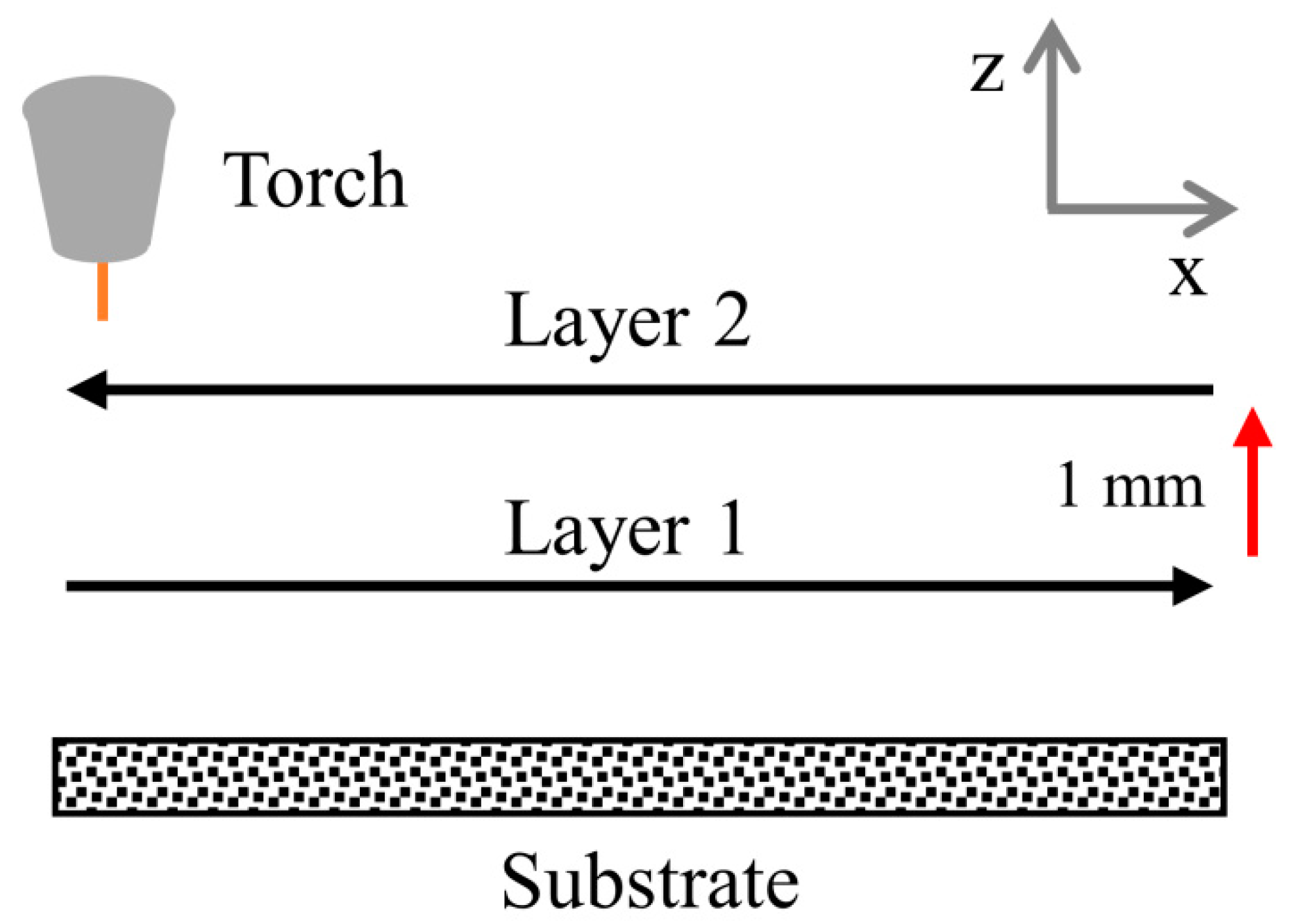
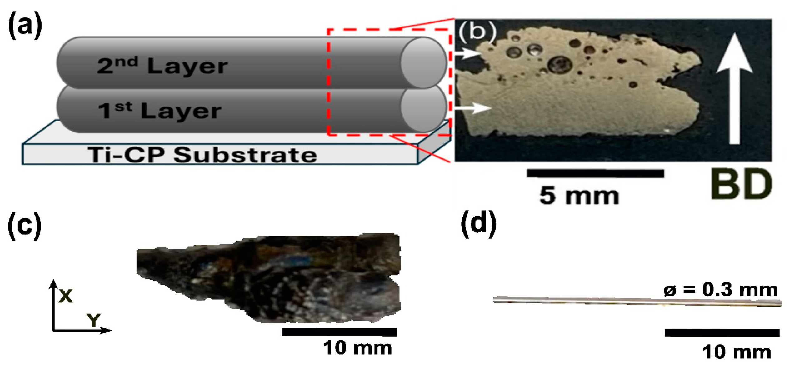
2.2. Fabrication of the NiTi Parts

The GMAW-based µ-WA-DED setup was employed for the fabrication of dual-layered NiTi components. Essentially, the µ-WA-DED prototype is composed of a customized welding torch, a 3-axis moving table, and an electrical circuit associated with a CITOWAVE III 520 power supply. A customized shielding gas feeder was also manufactured to protect the molten pool from oxidation within a radius of 2 mm, operating with a contact-tip-to-work distance of 5 mm. The deposition was performed using high-purity argon (Ar) gas (99.99%) at 15 L/min feeding rate. More information on the µ-WA-DED setup can be found in ref. [45].
A two-layer wall, with a width equivalent to a single bead and dimensions of approximately 20 × 2 × 3 mm3 (length × width × height), was deposited onto a substrate at room temperature using the processing parameters shown in Table 2. The bidirectional deposition strategy was employed for the fabrication of the wall, as illustrated in Figure 1. The successive overlapped beads were deposited discontinuously, and a 1 mm increment was added to the Z-axis before initiating the deposition of the second bead. No preheating was applied to the substrate. It is important to highlight that two layers are sufficient to carry out the experimental investigations in this work, i.e., the microstructure identification, layer-to-layer bonding analysis, and extraction of the thermal and mechanical behavior of NiTi walls produced by µ-WA-DED using a 0.3 mm NiTi wire. The properties of the finished part are not explored in this work.

2.3. Characterization of the Printed NiTi Parts

The NiTi parts were characterized in the as-deposited condition. The microstructure of the NiTi parts was analyzed in a plane parallel to their longitudinal section (X-Z plane in Figure 1). The printed parts were prepared using conventional metallographic techniques (mounting in Bakelite, grinding, and polishing). A solution of 10 mL of hydrofluoric acid (HF), 25 mL of nitric acid (HNO3), and 150 mL of water (H2O) was used to reveal the microstructure as suggested by the ASTM E407-07 standard [46], employing an etching time around 5–10 s.
Stereographic microscopy and optical microscopy (OM) techniques were used to identify porosity, determine indentation test locations, and measure the thickness of the deposited layers. Specifically, a stereographic microscope (Olympus BX51M-DP72) and an optical microscope (Nikon LV-100) with epi-illumination were employed. The microstructure in the deposited layers was analyzed by Scanning Electron Microscopy (SEM) using a Field Emission (FE) gun (FESEM). For this, a Zeiss Ultra 55 microscope was used. The images were captured on the cross-section of the samples using the backscattered electron (BSE) mode. The chemical analysis of the phases was performed by Energy Dispersive X-Ray Spectroscopy (EDS) using an X-ray detector (EDS, Oxford Instruments) coupled to the FESEM microscope.
The study of crystalline phases generated in both layers was conducted by X-ray diffraction (XRD) technique at 25 °C (room temperature), using a diffractometer (Panalytical X’pert pro) with Cu Kα radiation in Bragg–Brentano θ/θ configuration and Ni filter. The range of the angular analysis in 2θ was from 25° to 85° with steps of 0.02°and 1s per step.
The thermal analysis of the raw material (NiTi wire) and printed NiTi part was performed by Differential Scanning Calorimetry (DSC) using a TA Instruments Q20 calorimeter equipped with a liquid nitrogen cooling system and the Advantage™ software. The DSC analysis was performed over a temperature range from −120 °C to 120 °C with a heating/cooling rate of 10 K min−1. The initial and final temperatures of the martensitic transformation (B19′ ⇌ B2) were extracted from the peak in the DSC curves using the tangent method (ASTM F2004-05 [47]). The Advantage™ software v5.5.22 was used in this work to conduct the experiments, record results, and perform calculations.
The O, N, and H contents in the printed parts were determined by the inert gas fusion method using a LECO apparatus (model ONH-836), graphite crucible, and nickel capsule. These values correspond to the average value of the three measurements.
The hardness (H) and Young’s modulus (E) in different regions of the printed layers were obtained by instrumented indentation technique using a G-200 Nanoindenter (Agilent Technologies, Santa Clara, CA, USA). Indentations were performed with a Berkovich geometry tip whose area function was previously calibrated using a fused silica sample. Tests were carried out using the Continuous Stiffness Measurement (CSM) mode at a constant depth [48]. Different test strategies were carried out, summarized as (1) a linear array of indentations profile, starting at the top of the second layer (2nd layer) and finishing at the bottom of the first layer (1st layer). This profile was useful to reveal variations in the mechanical behavior along the cross-section of layers, allowing us to predict and interpret possible compositional/microstructural variations and interlayer interaction effects. (2) Several square arrays of 7 × 7 and 10 × 10 indentations were performed in different regions of each layer. These localized tests were used to analyze the mechanical features of the single phases/microstructures. Indentations were carried out at a constant depth of 1000 nm and spaced 20 µm apart. Finally, (3) a linear array of 50 indentations was employed at a constant depth of 500 nm and spaced 1 µm apart, focusing on the interlayer region. Here, a profound study of the transition region was performed.

3. Results and Discussion

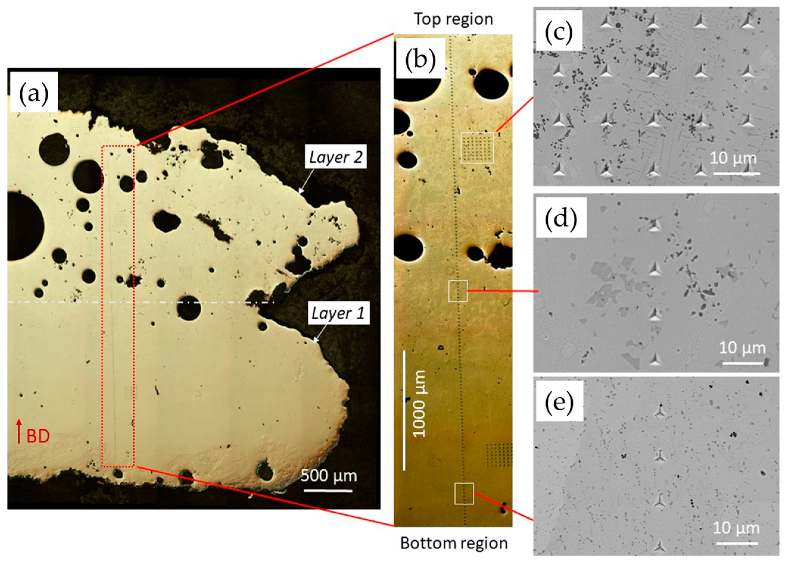
3.1. Metallurgical Characterization

Figure 2 shows the stereographic microscopy images of the printed NiTi part cross-section, confirming a good metallurgical joint between layers. Dispersed small pores were observed in the 1st layer, while bigger pores were observed in the 2nd layer. The rounded geometry of the pores indicates that their formation occurred due to gas entrapment during the deposition procedure. Many variables may have contributed to this formation. Depending on the processing parameters used during the WA-DED process, the high heat input can cause overheating on the raw material and consequently reach temperatures above the vaporization temperature of the base materials, mainly nickel [31,49], contributing to an increase in turbulence of liquid material. This effect, combined with factors such as the Marangoni current in the melted area, the fast solidification rate in addition to a possible gas shielding deficiency, may have facilitated the gaseous formation of contaminants such as O, N, and H. These contaminants can be found on the surface of the first layer, which could have mixed into the second layer during remelting. This phenomenon is commonly observed in techniques with a heat source based on focused high-energy lasers, where the energy input is more directed, causing evaporation and agitation of the flow of material found along the laser scan, leaving a characteristic trail of porous formation just below the construction surface [50,51]. However, this work used the same processing parameters in both layers. On the other hand, the short cooling time between the layers may have been insufficient to reach the room temperature in the 1st layer, which encourages higher overheating in the 2nd layer, followed by rapid solidification of the weld pool. In this short solidification time, it was impossible for gasses from the melting pool to escape.
Regarding how to avoid the formation of these pores, Pellone et al. [52] observed a significant reduction in porosity using He atmosphere instead of Ar in the weld region of aluminum alloys. Kim and Ahn (2011) [53], showed that a protective gas mixture of Ar-He (50:50 in vol.), flowing of up to 20 L/min, can also contribute to reduce porosity. Using NiTi alloy in the LMD Process, Malukhin and Ehmann (2006) [54] observed the absence of porosity with Ar shielding gas flows of around 17 L/min. Thus, using He shielding gas (pure or mixed with Ar) or increasing the Ar flow rate, allied to the higher delay time between consecutive layers, can be effective in avoiding pores formation in the L-PBF process. In the case of WA-DED, Liu et al. [55] achieved favorable metallurgical results by employing high-purity Ar shielding gas at a flow rate of 20 L/min, maintained for 90 s after deposition.

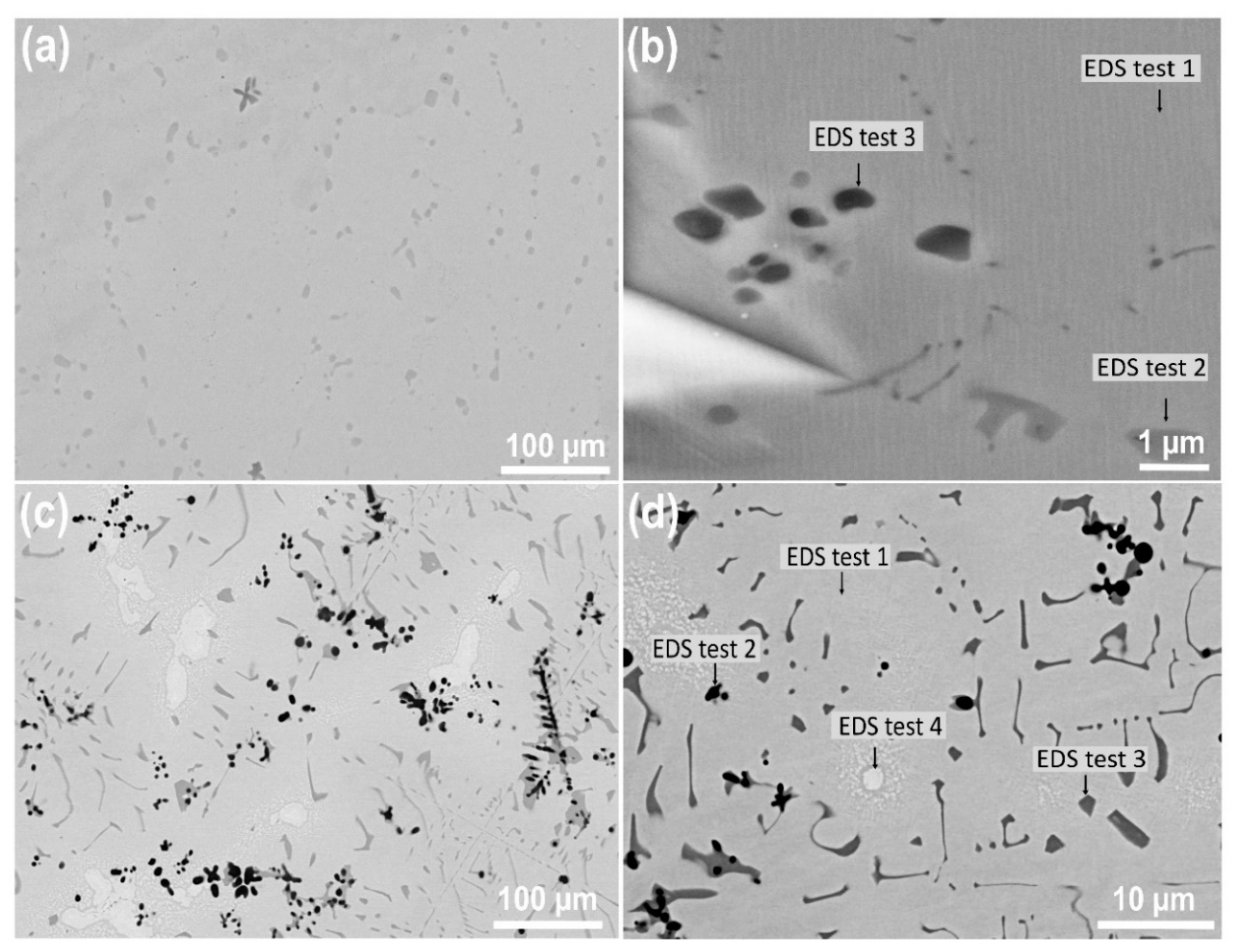
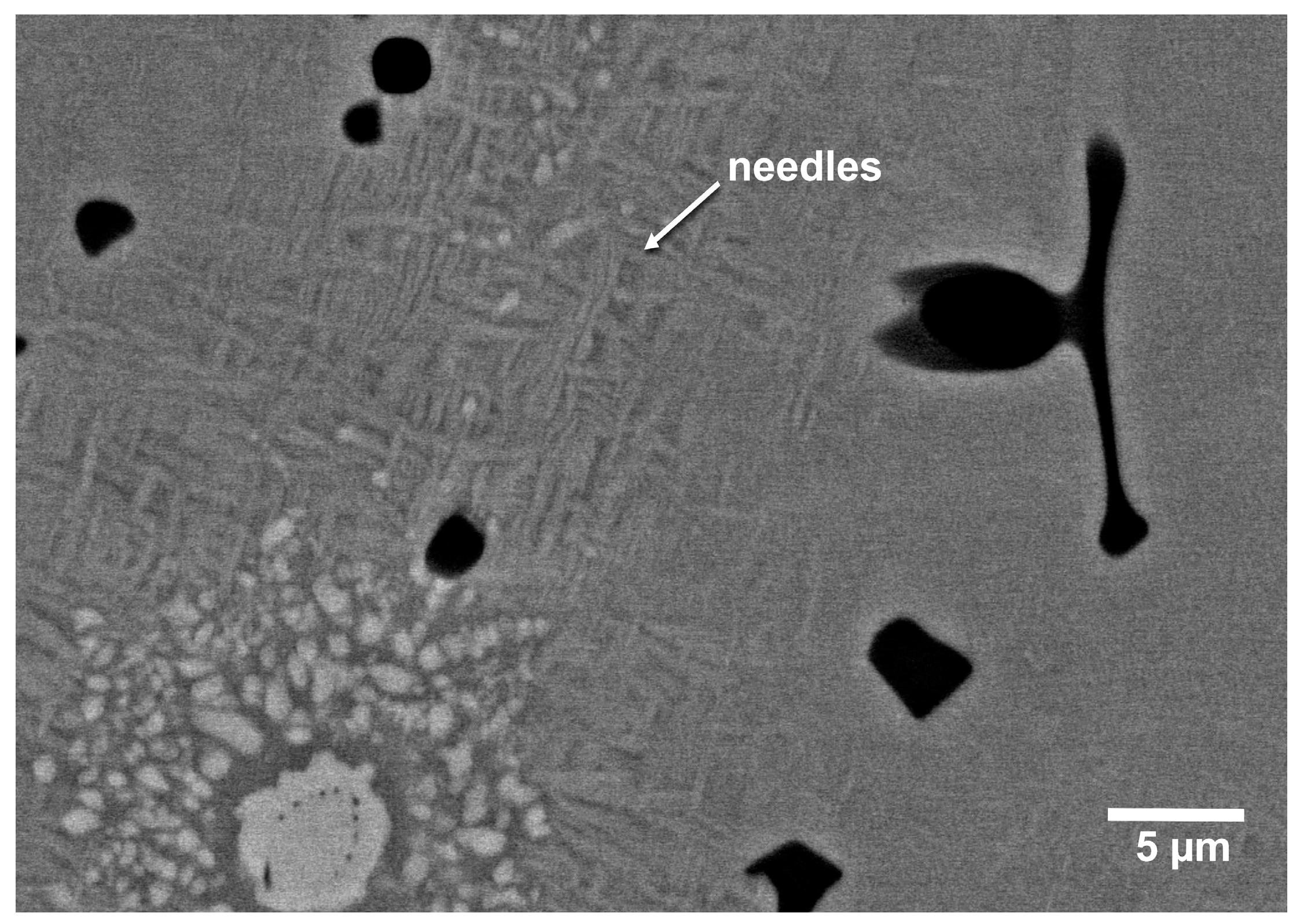
3.2. Microstructure and Chemical Characterization
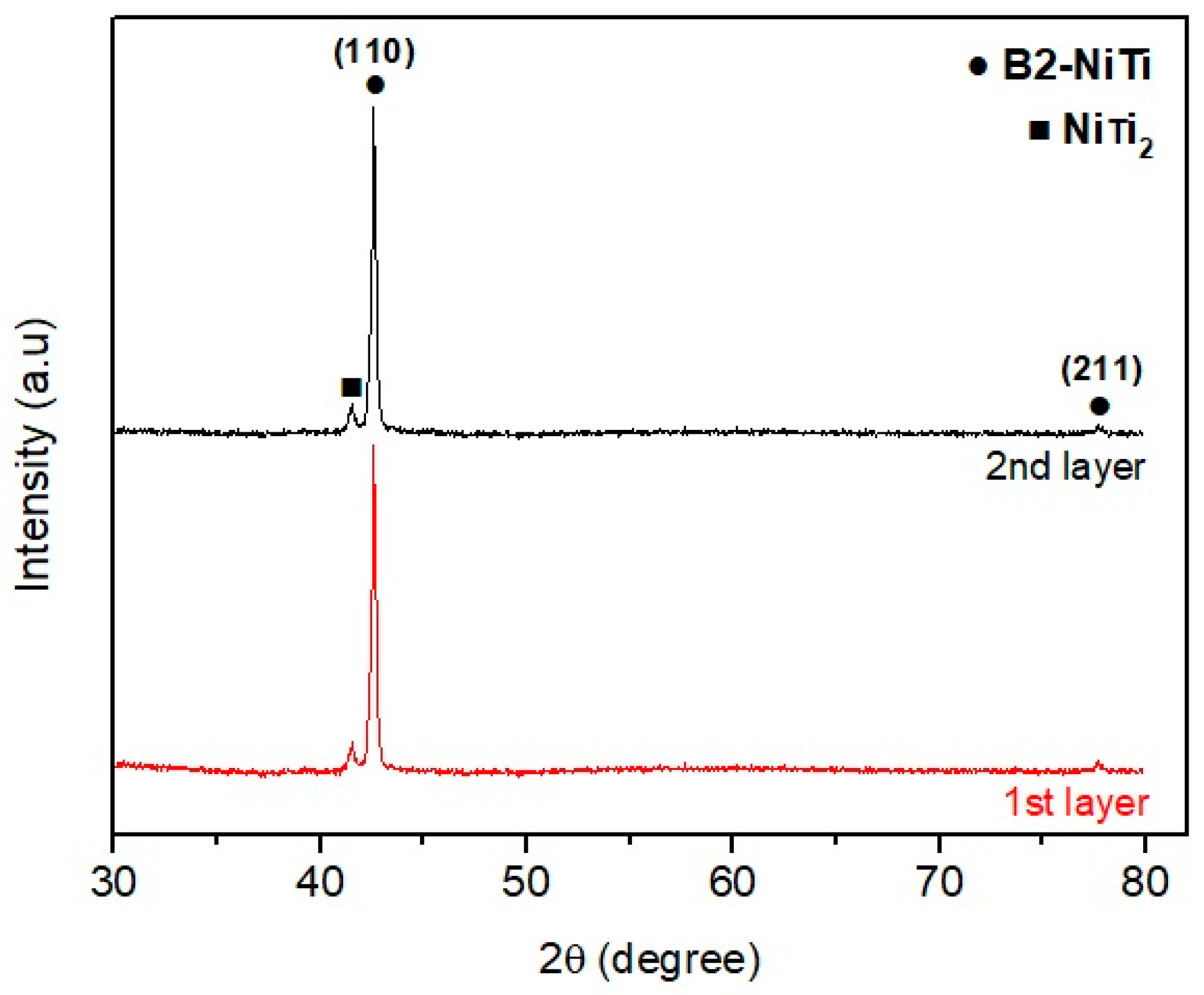
Figure 3 shows the FESEM-BSE images of the microstructure in the 1st and 2nd layers without chemical etching. In the 1st layer (Figure 3a,b), the presence of a small amount of fine Ni-poor phase was observed with mainly globular morphology (darker region) immersed in a Ni-rich matrix (brighter region). In the 2nd layer (Figure 3c,d), at least three phases were observed with different morphology (dendritic, lamellar, and equiaxial) and chemical composition (different shades of gray) in addition to the matrix phase.
The EDS analysis was carried out on the regions with different contrasts in the 1st and 2nd layers, as indicated in Figure 3b,d, respectively. The chemical composition obtained by the EDS analysis is summarized in Table 3. The EDS analysis revealed that the Ni content in the matrix of the 1st layer (point 1) was around 55 wt%, while 57.6 wt% was measured in the 2nd layer (point 1). Therefore, a Ni-rich matrix phase was obtained in both layers and its chemical composition was close to the composition of the raw wire (Ni56Ti44). However, segregation upon solidification, precipitation of secondary phases, or preferential evaporation of elements may cause local changes in the Ni content of the matrix [30]. Thus, a secondary phase was identified in the 1st layer (Figure 3b—test 2) with a slight difference in Ni content compared to the matrix (Figure 3b—test 1). Due to chemical composition similarity, allied with information from the Ti-Ni phase diagram and literature reports [56,57], the matrix could be associated with the B2-NiTi phase. Furthermore, the secondary phase denoted by point 3 (Figure 3b,d—test 3) presented a chemical composition close to the NiTi2 intermetallic phase (~38 wt% Ni) in both layers, with Ni content lower than the Ni content of the matrix. A secondary phase was identified in the 2nd layer, with Ni content around 70 wt% (Figure 3d—point 4), which was higher than the Ni content of the matrix; this phase could be associated with the Ni3Ti phase. Finally, a secondary phase was also detected in the 2nd layer with low Ni content (Figure 3d—point 2). It is worth mentioning that the low β stabilizer content (Ni) allied with the presence of interstitial elements (N and O), which were considered strong α-stabilizers, could stabilize the α-Ti phase at room temperature. The presence of a secondary phase with dendritic morphology in the microstructure of the 2nd layer indicates that this layer cooled at a lower solidification rate if compared to the 1st layer. This agrees with the higher overheating process found in the 2nd layer, which caused a decrease in the cooling rate.
Figure 4 shows more details about the microstructure in the 2nd layer of the NiTi part. Some needles were observed around the Ni3Ti phase at a very low volume fraction, which could be associated with the martensitic B19′-NiTi phase.

3.3. Phase Analysis

To empirically verify the phases present in the bilayer system, an X-ray diffraction study was carried out. Figure 5 depicts the XRD patterns of the 1st and 2nd layers of the NiTi part obtained by a diffraction plane parallel to its longitudinal ax. The 1st and 2nd layer diffraction peaks attributed to cubic Pm3m structure (ICDD PDF 65-917) were observed, corresponding to the austenite phase (B2-NiTi). Additionally, the primary diffraction peak of a cubic Fd3m structure (ICDD PDF 18-898) was also observed in both layers, indicating the presence of the intermetallic phase (NiTi2). The identification of the B2-NiTi and NiTi2 phases via XRD aligns with the FESEM-BSE analysis. The higher integrated intensity of the diffraction peaks of the B2-NiTi phase suggests the volumetric predominance of this phase in the microstructure of both layers. On the other hand, the low integrated intensity or absence of diffraction peaks associated with the NiTi2 phase, as well as the α-Ti, B19′-NiTi, and Ni3Ti phases, respectively, confirms the observed microstructure in FESEM-BSE images of the 2nd layer that could be due to its lower volumetric fraction.
NiTi2 phase is commonly encountered in Ni-rich NiTi alloys [58,59] and in NiTi SMA wire that has not undergone annealing. However, the NiTi2 phase can be dissolved within the NiTi matrix through a post-heat treatment [21,60,61].

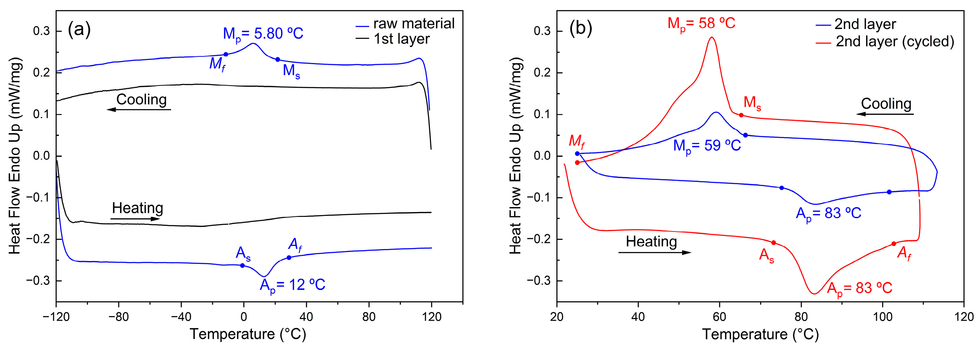
3.4. Phase-Transformation Behavior

The shape memory ability of the material is analyzed through the observation of the phase transformations and their temperatures. The NiTi part was analyzed by DSC aiming to detect the martensitic transformation (B19′ ⇌ B2), which determines the existence of the presence of the SME in the studied material. The DSC curves of the two layers in the NiTi part are depicted in Figure 6.
No martensitic transformation peak was detected in the sample of the 1st layer (Figure 6a). In contrast, peaks attributed to this transformation were observed during both heating (martensite decomposition: B19′ → B2) and cooling (martensite formation: B2 → B19′) processes in the sample of the 2nd layer (Figure 6b). These results support the FESEM-BSE analysis since the B19′-NiTi phase was only observed in the microstructure of the 2nd layer. The low integrated intensity of this peak suggests a minimal volumetric fraction of the B19′-NiTi phase in the microstructure. Furthermore, the integrated intensity of the martensitic transformation peak in the 2nd layer increased after the first thermal cycling. More studies will be necessary to clarify this point.
Data about phase-transformation temperatures extracted from the respective DSC curves are provided in Table 4, including Af measured on the finished wire. The preliminary tests by BFR conducted by the manufacturer on the finished wire showed that the Af temperature of the raw material is lower than room temperature (11.40 °C). The martensitic decomposition peak in NiTi wire shifted to a higher temperature in the 2nd layer of the NiTi part, increasing As and Af values from 4 °C to 76 °C and from 11 °C to 95 °C, respectively. In the 2nd layer, the formation of the Ni3Ti phase decreased the Ni content in the matrix [21,56,62]. It is well known that the martensitic transformation is sensitive to the variations in Ni content, e.g., Ms is inversely proportional to the Ni content in the matrix [63]. This explains the increase observed in martensitic transformation temperatures in the 2nd layer. B2-B19′ transformation is suppressed in the 1st layer due to the lack of nucleation sites [64], likely caused by microstructural changes, annealing, and increased energy barriers from repeated thermal cycling.
Table 5 shows the interstitial elements content (O, N, and H) in the 1st and 2nd layers of the NiTi part determined by the inert gas fusion method and reference values extracted from the ASTM F2063 standard [65]. The O and N contents of the layers of the NiTi part were higher than their nominal values in the ASTM F2063 standard, while the H content was in good agreement with this standard. The higher O and N contents in the NiTi part when compared to the raw material indicate a slight contamination by interstitial elements (O and N) during the µ-WA-DED processing, despite using a protective argon atmosphere. The 2nd layer presented a N and O content slightly higher than the 1st layer, due to the higher overheating and respective lower cooling rate during the deposition of the 2nd layer.

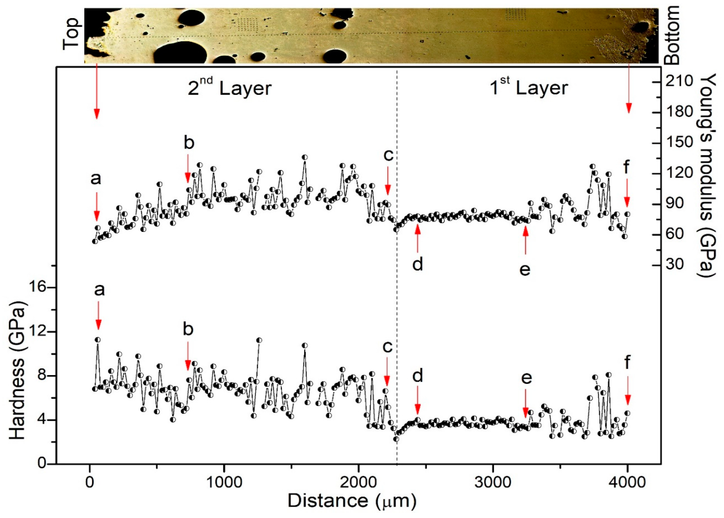
3.5. Mechanical Properties Characterization

To study the mechanical response of both layers and the influence of their phases/microstructures, different indentation tests were carried out. Figure 7 shows the optical microscope (OM) and FESEM-BSE images of the NiTi part with imprints performed on its surface. This analysis strategy aimed to correlate the microstructure observed by microscopy techniques in each layer with the hardness (H) and Young’s modulus (E) values obtained by instrumented indentation.
Figure 8 shows the E and H profiles obtained by the cross-section array indentations performed from the top side of the 2nd layer to the bottom side of the 1st layer. It was possible to differentiate one layer from the other since it was observed, in the 2nd layer, that there were higher E and H values than in the 1st layer. The high E and H values acquired in the 2nd layer could be explained by (1) the high N and O content in the 2nd layer, which caused solid solution hardening; and (2) the presence of intermetallic phases with a higher volume fraction in this region, which caused a deformation zone of indentation with lower contribution of the matrix and, consequently, with higher E and H values. These hypotheses are in accordance with the highest dispersion of results observed in the second-layer analysis.
The line base of H and E profiles in both layers can be associated with the predominant phase in the microstructure, which is the matrix of the B2-NiTi phase. Considering the region from d to e in the 1st layer, a constant profile of E and H was observed, resulting in approximate values of 75 GPa and 4 GPa, respectively. These values were higher than those reported in the literature for the B2-NiTi phase [66,67], since the O and N contamination can increase the E and H values. Considering the region from b to c in the 2nd layer, the average values of E and H around 100 GPa and 7 GPa, respectively, were obtained in the baseline. On the other hand, the variation in E and H values extracted in the baseline of both layers can be related to the presence of secondary phases (NiTi2, Ni3Ti, α-Ti) and/or inclusions. As expected, the 2nd layer presented higher dispersion of E and H than the 1st layer, due to the more complex microstructure that can be found in the 2nd layer. Furthermore, a singular behavior was observed in the E and H values in regions close to the top of the 2nd layer (from a to b) and close to the bottom of the 1st layer (from e to f), which can be associated with higher O contamination of the material and the atomic diffusion of the CP-Ti substrate, respectively.
The region between the c and d points in Figure 8 corresponds to the transition between 1st and 2nd layers, resulting in an abrupt change. An in-depth study of this region was conducted by analyzing the E and H values using a smaller spacing between indentations and deeper indentation depths than those used in the linear array test. This study showed that the transition region is narrow, and constrained to around 20 µm, as shown in the E and H profiles of Figure S1 available in the Supplementary Material.
To investigate the mechanical response of single phases in the respective microstructure, bidimensional arrays of indentations were performed into (d–e) and (b–c) regions of the 1st and 2nd layers, respectively. Figure 9 shows the E and H results from histogram plots to clarify the discussion. These results were obtained in both layers. In the 1st layer, a single distribution was observed in both histograms, which can be associated with the B2-NiTi phase, with a peak centered at E = 70 GPa and H = 3.8 GPa (Figure 9a,b, respectively). In the 2nd layer, at least 3 distributions were observed in the E and H histograms (Figure 9c,d, respectively). These distributions were easier to detect in the H histogram (see Figure 9d), as expected, due to the minor stress field volume generated by H in comparison with E [68]. This result indicates that the second layer is multiphasic.
Table 6 summarizes the E and H results and their correlation with the crystalline phases observed by FESEM-BSE. According to Li et al. (2017) [69], the E and H values of the observed phases in NiTi alloy should decrease in the following order: Ni3Ti > B2-NiTi > B19′-NiTi > NiTi2. Due to its lower volumetric fraction, the influence of the B19′-NiTi phase in the E and H values could be ignored. Thus, the correlation between the crystalline phase and the E and H values shown in Table 6 follows the previous order. Furthermore, the α-Ti phase stabilized by the high N and O contents presented E values close to CP-Ti but with higher H value.

4. Conclusions

The present work addressed the experimental investigation of the macroscopic morphology, microstructure evolution, phase transformation, and mechanical properties of NiTi shape memory alloys fabricated by the µ-WA-DED technique using a Ni-rich NiTi wire. Each deposited layer was extensively analyzed in this paper, leading to the following key findings:
Metallurgical Characterization: Strong metallurgical bonding was observed in the deposited layers of the printed NiTi-based part, with the first layer exhibiting small pores, while larger pores appeared in the subsequent layer, suggesting gas entrapment during deposition;
Phase Analysis: XRD and DSC techniques demonstrated the presence of austenite as the main constituent phase at room temperature. B19′ ⇌ B2 phase transformations occurred only during the heating and cooling processes of the second layer, while no martensitic phase transformation was observed in the first layer. Additionally, variations in the chemical composition of the second layer, such as slightly elevated N and O content which can be attributed to higher heat input and slower cooling rates during deposition, contributed to the increase in martensitic transformation temperatures in this layer;
Mechanical Properties: Variations in Young’s modulus and hardness among various phases and layers were revealed by instrumented indentation experiments, mainly influenced by microstructural and compositional heterogeneities;
Overall Performance: The layers exhibited excellent interlayer bonding, despite the observed porosity (as shown in Figure 2 and Figure 7). Additionally, this work outlines a pioneering effort to fabricate NiTi parts using a 0.3 mm wire, conditions that have not been previously investigated in the literature or industry.
These findings provide critical insights into the thermomechanical behavior of NiTi components fabricated by µ-WA-DED (using a 0.3 mm wire) and outline opportunities for optimizing AM processes to enhance material properties and performance. Although µ-WA-DED is still under development, results demonstrate that this technique can manufacture parts with excellent layer-to-layer bonding. Future research will focus on fabricating multi-layer NiTi components with complex geometries, aiming for improved dimensional accuracy and enhanced thermomechanical properties.

Supplementary Materials

The following supporting information can be downloaded at https://www.mdpi.com/article/10.3390/jmmp9020057/s1; Figure S1. Hardness and elastic modulus values were obtained by instrumented indentation on the transition region between consecutive layers.

Author Contributions

Conceptualization, T.C.d.S.; methodology, T.C.d.S.; validation, T.C.d.S.; formal analysis, T.C.d.S., E.S.-L., E.R., D.D.L., P.H.G.D. and T.G.S.; investigation, T.C.d.S.; resources, T.C.d.S.; data curation, T.C.d.S., E.S.-L., D.D.L., E.R., C.T.S., P.H.G.D. and J.C.A.D.F.; writing—original draft preparation, T.C.d.S., J.C.A.D.F. and D.D.L.; writing—review and editing, T.C.d.S., E.S.-L., E.R., C.T.S., J.C.A.D.F., N.V., P.H.G.D., S.S.M.T. and T.G.S.; visualization, T.C.d.S. and J.C.A.D.F.; supervision, T.C.d.S., S.S.M.T. and T.G.S.; project administration, T.C.d.S. and T.G.S.; funding acquisition, T.C.d.S., C.T.S., N.V., S.S.M.T. and T.G.S. All authors have read and agreed to the published version of the manuscript.

Funding

This research was funded by Carlos Chagas Filho Foundation for Research Support of Rio de Janeiro State (Fundação Carlos Chagas Filho de Amparo à Pesquisa do Estado do Rio de Janeiro—FAPERJ in Portuguese), grant E-26/210.349/202.

Data Availability Statement

Dataset available on request from the authors.

Acknowledgments

P.D. acknowledges FCT—MCTES for funding the PhD grant 2021.05298.BD. T.S. (Tadeu Silva) thanks MCTI/SISNANO/INT-CENANO-CNPQ (Process N° 442604/2019) for the SEM analysis. E.S.L. gratefully acknowledges the Brazilian National Research Council (CNPq, Brazil) for granting a postdoctoral research fellowship (Grant N° 302115/2021-8). T.G.S. acknowledges Portuguese Fundação para a Ciência e a Tecnologia (FCT—MCTES) for its financial support via the project UIDB/00667/2020 and UIDP/00667/2020 (UNIDEMI).

Conflicts of Interest

The authors declare no conflicts of interest.

References

  1. Patil, D.; Song, G. Shape memory alloy actuated accumulator for ultra-deepwater oil and gas exploration. Smart Mater. Struct. 2016, 25, 045012. [Google Scholar] [CrossRef]
  2. Özkul, İ.; Kurgun, M.A.; Kalay, E.; Canbay, C.A.; Aldaş, K. Shape memory alloys phenomena: Classification of the shape memory alloys production techniques and application fields. Eur. Phys. J. Plus 2019, 134, 585. [Google Scholar] [CrossRef]
  3. Manik, R.; Sahu, M.R. Biocompatibility of NiTi. Nickel-Titanium Smart Hybrid Materials; Elsevier: Amsterdam, The Netherlands, 2022; pp. 173–190. [Google Scholar] [CrossRef]
  4. Otsuka, K.; Ren, X. Physical metallurgy of Ti–Ni-based shape memory alloys. Prog. Mater. Sci. 2005, 50, 511–678. [Google Scholar] [CrossRef]
  5. Tadaki, T.; Otsuka, K.; Shimizu, K. Shape Memory Alloys. Annu. Rev. Mater. Sci. 1988, 18, 25–45. [Google Scholar] [CrossRef]
  6. Perkins, J. (Ed.) Shape Memory Effects in Alloys; Springer Science & Business Media: Berlin/Heidelberg, Germany, 2012. [Google Scholar]
  7. Otsuka, K.; Wayman, C.M. Shape Memory Materials; Cambridge University Press: Cambridge, UK, 1999. [Google Scholar]
  8. Gontijo, M.; da Silva, E.P.; de Castro, M.C.S.; dos Santos, C.T.; da Silva, T.C. Influence of deep cryogenic treatment on the pseudoelastic behavior of the Ni57Ti43 alloy. Shap. Mem. Superelasticity 2022, 8, 215–225. [Google Scholar] [CrossRef]
  9. Sehitoglu, H.; Wu, Y.; Patriarca, L.; Li, G.; Ojha, A.; Zhang, S.; Chumlyakov, Y.; Nishida, M. Superelasticity and shape memory behavior of NiTiHf alloys. Shape Mem. Superelasticity 2017, 3, 168–187. [Google Scholar] [CrossRef]
  10. Ghosh, P.; Rao, A.; Srinivasa, A.R. Design of multi-state and smart-bias components using shape memory alloy and shape memory polymer composites. Mater. Des. 2013, 44, 164–171. [Google Scholar] [CrossRef]
  11. Huang, W. On the selection of shape memory alloys for actuators. Mater. Des. 2002, 23, 11–19. [Google Scholar] [CrossRef]
  12. Kim, H.-C.; Yoo, Y.-I.; Lee, J.-J. Development of a NiTi actuator using a two-way shape memory effect induced by compressive loading cycles. Sens. Actuators A Phys. 2008, 148, 437–442. [Google Scholar] [CrossRef]
  13. Elahinia, M.H.; Hashemi, M.; Tabesh, M.; Bhaduri, S.B. Manufacturing and processing of NiTi implants: A review. Prog. Mater. Sci. 2012, 57, 911–946. [Google Scholar] [CrossRef]
  14. Elahinia, M.; Moghaddam, N.S.; Andani, M.T.; Amerinatanzi, A.; Bimber, B.A.; Hamilton, R.F. Fabrication of NiTi through additive manufacturing: A review. Prog. Mater. Sci. 2016, 83, 630–663. [Google Scholar] [CrossRef]
  15. Dadbakhsh, S.; Speirs, M.; Van Humbeeck, J.; Kruth, J.-P. Laser additive manufacturing of bulk and porous shape-memory NiTi alloys: From processes to potential biomedical applications. MRS Bull. 2016, 41, 765–774. [Google Scholar] [CrossRef]
  16. Lu, H.Z.; Yang, C.; Luo, X.; Ma, H.W.; Song, B.; Li, Y.Y.; Zhang, L.C. Ultrahigh-performance TiNi shape memory alloy by 4D printing. Mater. Sci. Eng. A 2019, 763, 138177. [Google Scholar] [CrossRef]
  17. Mitchell, A.; Lafont, U.; Hołyńska, M.; Semprimoschnig, C. Additive manufacturing: A review of 4D printing and future applications. Addit. Manuf. 2018, 24, 606–626. [Google Scholar] [CrossRef]
  18. Frazier, W.E. Metal Additive Manufacturing: A Review. J. Mater. Eng. Perform. 2014, 23, 1917–1928. [Google Scholar] [CrossRef]
  19. Resnina, N.; Palani, I.A.; Belyaev, S.; Singh, S.; Kumar, A.; Bikbaev, R.; Sahu, A. Functional Properties of the Multilayer NiTi Alloy Produced by Wire Arc Additive Manufacturing. Shap. Mem. Superelasticity 2022, 8, 5–15. [Google Scholar] [CrossRef]
  20. Farber, E.; Zhu, J.-N.; Popovich, A.; Popovich, V. A review of NiTi shape memory alloy as a smart material produced by additive manufacturing. Mater. Today Proc. 2020, 30, 761–767. [Google Scholar] [CrossRef]
  21. Yu, L.; Chen, K.; Zhang, Y.; Liu, J.; Yang, L.; Shi, Y. Microstructures and mechanical properties of NiTi shape memory alloys fabricated by wire arc additive manufacturing. J. Alloys Compd. 2022, 892, 162051. [Google Scholar] [CrossRef]
  22. Sun, S.; Brandt, M.; Easton, M. Powder bed fusion processes: An overview. Laser Additive Manufacturing; Woodhead Publishing: Sawston, UK, 2017; pp. 55–77. [Google Scholar]
  23. Svetlizky, D.; Das, M.; Zheng, B.; Vyatskikh, A.L.; Bose, S.; Bandyopadhyay, A.; Schoenung, J.M.; Lavernia, E.J.; Eliaz, N. Directed energy deposition (DED) additive manufacturing: Physical characteristics, defects, challenges and applications. Mater. Today 2021, 49, 271–295. [Google Scholar] [CrossRef]
  24. Bayati, P.; Jahadakbar, A.; Barati, M.; Nematollahi, M.; Saint-Sulpice, L.; Haghshenas, M.; Chirani, S.A.; Mahtabi, M.J.; Elahinia, M. Toward low and high cycle fatigue behavior of SLM-fabricated NiTi: Considering the effect of build orientation and employing a self-heating approach. Int. J. Mech. Sci. 2020, 185, 105878. [Google Scholar] [CrossRef]
  25. Otubo, J.; Rigo, O.D.; Neto, C.M.; Mei, P.R. The effects of vacuum induction melting and electron beam melting techniques on the purity of NiTi shape memory alloys. Mater. Sci. Eng. A 2006, 438–440, 679–682. [Google Scholar] [CrossRef]
  26. Lu, B.; Cui, X.; Jin, G.; Dong, M.; Fang, Y.; Ma, W. Effect of La2O3 addition on mechanical properties and wear behaviour of NiTi alloy fabricated by direct metal deposition. Opt. Laser Technol. 2020, 129, 106290. [Google Scholar] [CrossRef]
  27. Krishna, B.V.; Bose, S.; Bandyopadhyay, A. Fabrication of porous NiTi shape memory alloy structures using laser engineered net shaping. J. Biomed. Mater. Res. B 2009, 89b, 481–490. [Google Scholar] [CrossRef] [PubMed]
  28. Rodrigues, T.A.; Duarte, V.; Miranda, R.M.; Santos, T.G.; Oliveira, J.P. Current Status and Perspectives on Wire and Arc Additive Manufacturing (WAAM). Materials 2019, 12, 1121. [Google Scholar] [CrossRef] [PubMed]
  29. Ke, W.C.; Oliveira, J.P.; Cong, B.Q.; Ao, S.S.; Qi, Z.W.; Peng, B.; Zeng, Z. Multi-layer deposition mechanism in ultra-high-frequency pulsed wire arc additive manufacturing (WAAM) of NiTi shape memory alloys. Addit. Manuf. 2022, 50, 102932. [Google Scholar] [CrossRef]
  30. Treutler, K.; Wesling, V. The Current State of Research of Wire Arc Additive Manufacturing (WAAM): A Review. Appl. Sci. 2021, 11, 6474. [Google Scholar] [CrossRef]
  31. Zeng, Z.; Cong, B.Q.; Oliveira, J.P.; Ke, W.C.; Schell, N.; Peng, B.; Qi, Z.W.; Ge, F.G.; Zhang, W.; Ao, S.S. Wire and arc additive manufacturing of a Ni-rich NiTi shape memory alloy: Microstructure and mechanical properties. Addit. Manuf. 2020, 32, 101017. [Google Scholar] [CrossRef]
  32. Wang, J.; Pan, Z.; Yang, G.; Han, J.; Chen, X.; Li, H. Location dependence of microstructure, phase transformation temperature and mechanical properties on Ni-rich NiTi alloy fabricated by wire arc additive manufacturing. Mater. Sci. Eng. A 2019, 749, 218–222. [Google Scholar] [CrossRef]
  33. Khan, M.I.; Pequegnat, A.; Zhou, Y.N. Multiple memory shape memory alloys. Adv. Eng. Mater. 2013, 15, 386–393. [Google Scholar] [CrossRef]
  34. Oliveira, J.P.; Gouveia, F.M.; Santos, T.G. Micro wire and arc additive manufacturing (µ-WAAM). Addit. Manuf. Lett. 2022, 2, 100032. [Google Scholar] [CrossRef]
  35. Dornelas, P.H.G.; Santos, T.G.; Oliveira, J.P. Micro-metal additive manufacturing—State-of-art and perspectives. Int. J. Adv. Manuf. Technol. 2022, 122, 3547–3564. [Google Scholar] [CrossRef]
  36. Dornelas, P.H.G.; Oliveira, J.P.; da Silva, T.C.; Ramos, A.S.; Santos, T.G. Development of a gas metal arc-based prototype for direct energy deposition with micrometric wire. J. Mater. Res. Technol. 2024, 30, 3571–3583. [Google Scholar] [CrossRef]
  37. Cunningham, C.R.; Flynn, J.M.; Shokrani, A.; Dhokia, V.; Newman, S.T. Strategies and processes for high quality wire arc additive manufacturing. Addit. Manuf. 2018, 22, 672–686. [Google Scholar]
  38. Spears, T.G.; Gold, S.A. In-process sensing in selective laser melting (SLM) additive manufacturing. Integr. Mater. Manuf. Innov. 2016, 5, 16–40. [Google Scholar] [CrossRef]
  39. Dinovitzer, M.; Chen, X.; Laliberte, J.; Huang, X.; Frei, H. Effect of wire and arc additive manufacturing (WAAM) process parameters on bead geometry and microstructure. Addit. Manuf. 2019, 26, 138–146. [Google Scholar] [CrossRef]
  40. Jafari, D.; Vaneker, T.H.J.; Gibson, I. Wire and arc additive manufacturing: Opportunities and challenges to control the quality and accuracy of manufactured parts. Mater. Des. 2021, 202, 109471. [Google Scholar] [CrossRef]
  41. Wu, B.; Pan, Z.; Ding, D.; Cuiuri, D.; Li, H.; Xu, J.; Norrish, J. A review of the wire arc additive manufacturing of metals: Properties, defects, and quality improvement. J. Manuf. Process. 2018, 35, 127–139. [Google Scholar] [CrossRef]
  42. Kohl, M. Shape Memory Microactuators; Springer: Berlin/Heidelberg, Germany, 2004; pp. 62–95. [Google Scholar]
  43. ASTM F2082-03; Standard Test Method for Determination of Transformation Temperature of Nickel-Titanium Shape Memory Alloys by Bend and Free Recovery. ASTM International: West Conshohocken, PA, USA, 2017. Available online: https://www.astm.org/f2082-03.html (accessed on 1 July 2023).
  44. ASTM F67-13; Standard Specification for Unalloyed Titanium, for Surgical Implant Applications (UNS R50250, UNS R50400, UNS R50550, UNS R50700). ASTM: West Conshohocken, PA, USA, 2017.
  45. Dornelas, P.H.G.; Farias, F.W.C.; da Silva, T.C.; da Cruz Payão Filho, J.; Ramos, A.S.; Oliveira, J.P.; Santos, T.G. Stainless and low-alloy steels additively manufactured by micro gas metal arc-based directed energy deposition: Microstructure and mechanical behavior. Prog. Addit. Manuf. 2024. [Google Scholar] [CrossRef]
  46. ASTM E407-07; Standard Practice for Microetching Metals and Alloys. ASTM: West Conshohocken, PA, USA, 2016; 7.
  47. ASTM-F2004-05; Standard Test Method for Transformation Temperature of Nickel-Titanium Alloys by Thermal Analysis. ASTM International: West Conshohocken, PA, USA, 2010; p. 4.
  48. Carvalho, L.R.A.; Sallica-Leva, E.; Encinas, E.R.; Fogagnolo, J.B. Less-rigid coating in Ti obtained by laser surface alloying with Nb. Surf. Coat. Technol. 2018, 346, 19–28. [Google Scholar] [CrossRef]
  49. Resnina, N.; Palani, I.A.; Belyaev, S.; Singh, S.; Mani Prabu, S.S.; Bikbaev, R.; Jayachandran, S.; Kalganov, V. Peculiarities of the recoverable strain variation in the NiTi alloy produced by wire arc additive manufacturing. Mater. Lett. 2021, 298, 130004. [Google Scholar] [CrossRef]
  50. Du, C.; Zhao, Y.; Jiang, J.; Wang, Q.; Wang, H.; Li, N.; Sun, J. Pore defects in Laser Powder Bed Fusion: Formation mechanism, control method, and perspectives. J. Alloys Compd. 2023, 944, 169215. [Google Scholar] [CrossRef]
  51. Mugwagwa, L.; Yadroitsev, I.; Matope, S. Effect of process parameters on residual stresses, distortions, and porosity in selective laser melting of maraging steel 300. Metals 2019, 9, 1042. [Google Scholar] [CrossRef]
  52. Pellone, L.; Inamke, G.; Hong, K.M.; Shin, Y.C. Effects of interface gap and shielding gas on the quality of alloy AA6061 fiber laser lap weldings. J. Mater. Process. Technol. 2019, 268, 201–212. [Google Scholar] [CrossRef]
  53. Kim, C.H.; Ahn, D.C. Influence of process parameters on welding quality during lap welding of aluminum sheets using high brightness disk laser. Adv. Mater. Res. 2011, 264, 361–366. [Google Scholar] [CrossRef]
  54. Malukhin, K.; Ehmann, K. Material characterization of NiTi-based memory alloys fabricated by the laser direct metal deposition process. J. Manuf. Sci. Eng. 2006, 128, 691–696. [Google Scholar] [CrossRef]
  55. Liu, G.; Zhou, S.; Lin, P.; Zong, X.; Chen, Z.; Zhang, Z.; Ren, L. Analysis of microstructure, mechanical properties, and wear performance of NiTi alloy fabricated by cold metal transfer-based wire arc additive manufacturing. J. Mater. Res. Technol. 2022, 20, 246–259. [Google Scholar] [CrossRef]
  56. Song, D.; Wang, T.; Wei, L.; Jiang, S. Microstructure evolution and functional response of NiTi shape memory alloy manufactured by dual-wire electron beam freeform fabrication. J. Manuf. Process. 2024, 119, 842–855. [Google Scholar] [CrossRef]
  57. Teng, J.Z.; Jiang, P.F.; Cui, X.H.; Nie, M.H.; Li, X.R.; Liu, C.Z.; Zhang, Z.H. Revealing microstructural evolutions, mechanical properties and wear performance of wire arc additive manufacturing homogeneous and heterogeneous NiTi alloy. J. Mater. Res. Technol. 2023, 27, 1593–1610. [Google Scholar] [CrossRef]
  58. Tadayyon, G.; Mazinani, M.; Guo, Y.; Zebarjad, S.M.; Tofail, S.A.M.; Biggs, M.J.P. Study of the microstructure evolution of heat-treated Ti-rich NiTi shape memory alloy. Mater. Charact. 2016, 112, 11–19. [Google Scholar] [CrossRef]
  59. Pu, Z.; Du, D.; Wang, K.; Liu, G.; Zhang, D.; Zhang, H.; Xi, R.; Wang, X.; Chang, B. Study on the NiTi shape memory alloys in-situ synthesized by dual-wire-feed electron beam additive manufacturing. Addit. Manuf. 2022, 56, 102886. [Google Scholar] [CrossRef]
  60. Hamilton, R.F.; Bimber, B.A.; Palmer, T.A. Correlating microstructure and superelasticity of directed energy deposition additive manufactured Ni-rich NiTi alloys. J. Alloys Compd. 2018, 739, 712–722. [Google Scholar] [CrossRef]
  61. Halani, P.R.; Kaya, I.; Shin, Y.C.; Karaca, H.E. Phase transformation characteristics and mechanical characterization of nitinol synthesized by laser direct deposition. Mater. Sci. Eng. A. 2013, 559, 836–843. [Google Scholar] [CrossRef]
  62. Khoo, Z.X.; Liu, Y.; An, J.; Chua, C.K.; Shen, Y.F.; Kuo, C.N. A review of selective laser melted NiTi shape memory alloy. Materials 2018, 11, 519. [Google Scholar] [CrossRef] [PubMed]
  63. Khalil-Allafi, J.; Dlouhy, A.; Eggeler, G. Ni4Ti3-precipitation during aging of NiTi shape memory alloys and its influence on martensitic phase transformations. Acta Mater. 2002, 50, 4255–4274. [Google Scholar] [CrossRef]
  64. Chen, Z.; Qin, S.; Shang, J.; Wang, F.; Chen, Y. Size effects of NiTi nanoparticle on thermally induced martensitic phase transformation. Intermetallics 2018, 94, 47–54. [Google Scholar] [CrossRef]
  65. ASTM F2063-18; Standard Specification for Wrought Nickel-Titanium Shape Memory Alloys for Medical Devices and Surgical Implants. ASTM International: West Conshohocken, PA, USA, 2018.
  66. Šittner, P.; Heller, L.; Pilch, J.; Curfs, C.; Alonso, T.; Favier, D. Young’s Modulus of Austenite and Martensite Phases in Superelastic NiTi Wires. J. Mater. Eng. Perform. 2014, 23, 2303–2314. [Google Scholar] [CrossRef]
  67. Gall, K.; Juntunen, K.; Maier, H.J.; Sehitoglu, H.; Chumlyakov, Y.I. Instrumented micro-indentation of NiTi shape-memory alloys. Acta Mater. 2001, 49, 3205–3217. [Google Scholar] [CrossRef]
  68. Niklas, A.; Santos, F.; Garcia, D.; Rouco, M.; González-Martínez, R.; Pereira, J.C.; Rayón, E.; Lopez, P.; Guillonneau, G. Chemical composition effects on the microstructure and hot hardness of NiCrSiFeB self-fluxing alloys manufactured via gravity casting. J. Manuf. Mater. Process. 2023, 7, 196. [Google Scholar] [CrossRef]
  69. Li, Y.; Tang, S.; Gao, Y.; Ma, S.; Zheng, Q.; Cheng, Y. Mechanical and thermodynamic properties of intermetallic compounds in Ni-Ti system. Int. J. Mod. Phys. B 2017, 31, 1750161. [Google Scholar] [CrossRef]
Figure 1. Schematic representation of the employed deposition strategy that was used to manufacture the NiTi walls by µ-WA-DED.
Jmmp 09 00057 g001
Figure 2. (a) Schematic representation of the layer deposition with emphasis on the region analyzed by SEM, (b) cross-section along the longitudinal direction after metallographic preparation of the sample, (c) panoramic image of the printed NiTi part, and (d) 0.3 mm NiTi wire acquired from Fort Wayne Metals (Fort Wayne, IN, USA). BD: build direction.
Jmmp 09 00057 g002
Figure 3. FESEM-BSE images of the microstructure in the (a,b) 1st and (c,d) 2nd layer with (a,c) low and (b,d) high magnification, highlighting the EDS analysis locations in the higher magnification images (i.e., (b,d)).
Jmmp 09 00057 g003
Figure 4. FESEM-BSE high magnification image of the microstructure in the 2nd layer of the NiTi part.
Jmmp 09 00057 g004
Figure 5. XRD patterns of the 1st and 2nd layers of the NiTi part.
Jmmp 09 00057 g005
Figure 6. DSC curves of the NiTi part: (a) 1st layer; (b) 2nd layer and 2nd layer (cycled).
Jmmp 09 00057 g006
Figure 7. (a) OM image of the cross-section of the printed NiTi part. (b) OM magnified image of the red-rectangle region highlighted in (a), showing the location of nanoindentation imprints. (ce) FESEM-BSE images of the imprints localized in the two-dimensional array (c) and in the linear array (d,e).
Jmmp 09 00057 g007
Figure 8. Extracted E and H values of the NiTi part as a function of the distance from the top side of the 2nd layer, denoted by a, to the bottom side of the 1st layer, denoted by f.
Jmmp 09 00057 g008
Figure 9. E (a,c) and H (b,d) histograms of the NiTi part for the 1st (a,b) and 2nd (c,d) layer.
Jmmp 09 00057 g009
Table 1. Elemental chemical composition of NiTi wire and CP-Ti substrate.
CompositionNiTiCFeHONOthers
Wire (wt %)56.03bal.0.02840.0081<0.0050.0239-<0.2485
Substrate 1 (wt %)-bal.≤0.08≤0.30≤0.015≤0.25≤0.03-
1 ASTM F67-13 standard.
Table 2. Processing parameters that were used during the manufacturing process of the NiTi walls.
Travel Speed
(mm/s)
Current Peak (A)Arc Voltage
(V)
Wire Feed Speed
(mm/s)
Ar Flow Rate
(L/min)
47817.57.410
Table 3. EDS results of selected points in Figure 3b,d.
PositionElements (at%)
1st Layer2nd Layer
149.93 Ni + 50.07 Ti52.56 Ni + 47.44 Ti
249.82 Ni + 50.18 Ti07.21 Ni + 92.79 Ti
325.71 Ni + 74.29 Ti35.22 Ni + 64.78 Ti
4-62.66 Ni + 37.34 Ti
Table 4. Transformation temperatures of the as-received wire and the 2nd layer in the NiTi part.
MaterialsPhase Transformation Temperature (°C) 1
MsMpMfAsApAf
Wire (raw material)20.405.80−5.402.1012.0023.60
2nd layer64.6059.1424.9075.8083.0796.40
2nd layer cycled63.1458.0024.2076.2083.0095.80
1 The temperature error was on the order of ±1 °C.
Table 5. Interstitial elements content in the 1st and 2nd layers of NiTi part and reference values extracted from ASTM F2063 standard.
ElementAs-Received Wire
(wt %)
NiTi Part
(wt %)
ASTM F2063
(wt %)
1st Layer2nd Layer
Oxygen0.0239 ± 0.040.212 ± 0.0330.262 ± 0. 038max. 0.040
Nitrogen0.0004 ± 0.0260.066 ± 0.0080.0835 ± 0.0116max. 0.005
Hydrogen<0.005 ± 0.00080.0009 ± 0.00020.00114 ± 0.00004max. 0.005
Table 6. Summary of the E and H values measured in the 1st and 2nd layers (based on the results of Figure 9) and correlation with crystalline phases observed by FESEM-BSE.
LayerH (GPa)E (GPa)Phase
1st3.870B2-NiTi
2nd4.5-NiTi2
6.785B2-NiTi
8105α-Ti
15135Ni3Ti
Disclaimer/Publisher’s Note: The statements, opinions and data contained in all publications are solely those of the individual author(s) and contributor(s) and not of MDPI and/or the editor(s). MDPI and/or the editor(s) disclaim responsibility for any injury to people or property resulting from any ideas, methods, instructions or products referred to in the content.

