Review

Application of 3D and 4D Printing in Electronics

by
Matilde Aronne
1,*,
Miriam Polano
1,*,
Valentina Bertana
1,
Sergio Ferrero
1,
Francesca Frascella
2,
Luciano Scaltrito
1 and
Simone Luigi Marasso
1,3
1
Chilab-Materials and Microsystems Laboratory, Department of Applied Science and Technology (DISAT), Politecnico di Torino, Via Lungo Piazza d’Armi 6, 10034 Chivasso, Italy
2
Department of Applied Science and Technology (DISAT)—PolitoBIOMed Lab, Politecnico di Torino, Corso Duca degli Abruzzi, 24, 10129 Turin, Italy
3
National Research Council-Institute of Materials for Electronics and Magnetism (CNR-IMEM), Parco Area delle Scienze 37, 43124 Parma, Italy
*
Authors to whom correspondence should be addressed.
J. Manuf. Mater. Process. 2024, 8(4), 164; https://doi.org/10.3390/jmmp8040164
Submission received: 1 July 2024 / Revised: 18 July 2024 / Accepted: 21 July 2024 / Published: 31 July 2024
(This article belongs to the Topic Modern Technologies and Manufacturing Systems, 2nd Volume)

Abstract

:
Nowadays, additive manufacturing technologies have impacted different engineering sectors. Three- and four-dimensional printing techniques are increasingly used in soft and flexible electronics thanks to the possibility of working contemporarily with several materials on various substrates. The materials portfolio is wide, as well as printing processes. Shape memory polymers, together with composites, have gained great success in the electronic field and are becoming increasingly popular for fabricating pH, temperature, humidity, and stress sensors that are integrated into wearable, stretchable, and flexible devices, as well as for the fabrication of communication devices, such as antennas. Here, we report an overview of the state of the art about the application of 4D printing technologies and smart materials in electronics.

1. Introduction

The concept of applying printing methods to fabricate electronic devices originated in the 20th century, during the first attempts in flexible conductor manufacturing as printed circuit boards (PCB) became popular in the 1950s. However, the deposition of conductive inks on substrates to obtain conductive tracks was proposed only in the early 1990s. Together with this, the advent of new processing techniques has allowed the substitution of common rigid substrates for new, flexible substrates [1]. Printing technologies were introduced because they permitted the fabrication of large-area electronics at relatively low cost. Such lower investment costs depend on the reduced number of fabrication steps and decreased substrate and raw materials expenses. Printing technologies also guaranteed higher-throughput processes, which could then be easily automatized, allowing for the exploration of new alternatives for electronic devices [2]. This brief history of printed electronics provides insight into the subsequent transition to 3D and 4D printing of smart devices, like sensors, batteries, actuators, and soft electronics. These new fabrication technologies have gained ground not only because of the possibility they offer to avoid cleanroom processes but also because they offer (i) a one-tool manufacturing procedure; (ii) versatility in shape design and substrate choice, both in terms of being rigid and flexible; and (iii) the possibility to integrate different capabilities, length scales, and materials together [3].
The term “3D printing” encompasses all the additive manufacturing (AM) technologies enabling one-step, layer-by-layer fabrication, starting from a CAD model. As defined by the ISO/ASTM 52900:2021, AM technologies are all those processes of “joining materials to make parts […], usually layer upon layer, as opposed to subtractive manufacturing and formative manufacturing methodologies” [4]. AM has numerous advantages, like fast, flexible design and fabrication without moulds or tools, even of complex geometries, and a reduction in time-to-market. These advantages can be attributed to the fabrication of assemblies, the design intelligence, the reduction in the number of stages in the supply chain, the reduction in waste materials and costs, the simplicity of use, and the product personalization [5,6,7]. The evolution of 3D printing is the previously mentioned 4D printing. The fourth dimension, time, is now involved in the additive fabrication process result. Time is intended for the evolution over time of the shape or other properties of the printed elements due to the exposure to external stimuli (e.g., pH variation, temperature variation, light exposure, and water immersion).
In Table 1, the five factors responsible for 4D printing are reported; the sentence “The stimulus is applied on the smart material using a suitable interaction mechanism and mathematical modelling during an AM process which results into a 4D printed structure” perfectly embraces them all [8].
Considering the five elements of 4D printing, the involvement of each factor in the fabrication process of a dynamic structure is summarized in Figure 1.
This fabrication strategy ensures the fast growth of smart materials and multi-materials, allowing for deformable printed parts. Moreover, it permits high efficiency and performance, leading to a better quality of the final elements because of their ability to self-enhance their characteristics. According to Momeni et al., the changes in 4D printed structures can be classified into three categories [9]: self-assembly, multi-functionality (or self-adaptability), and self-repair. These modifications can be pre-programmed through the design phase and selecting the most appropriate materials, like shape memory polymers or composites [8].
As with 3D-printing technologies, 4D-printing technologies are gaining ground in different fields because of the products’ adaptability to environment variations, self-repairing capability, and self-assembly ability of the printed parts. Sectors like soft robotics and electronics are already experiencing the benefits of 4D printing. The aim of soft robotics is to develop robots that can overcome traditional robotics limitations, such as handling high deformation and enduring any environmental conditions. Soft robotics relies on the use of soft objects, materials, or systems to fabricate robots that meet the softness requirements of the environment or the receiver [10]. The work of Wehner et al. is an example of soft robots fabrication using 3D-printing technologies [11]. They fabricated a completely soft autonomous octobot where all the elements, like fuel channels, actuator controllers, etc., were embedded into an elastomeric matrix. Such 4D printing enabled the breakthrough of the already mentioned robotic limitations, fabricating soft robots using smart materials.
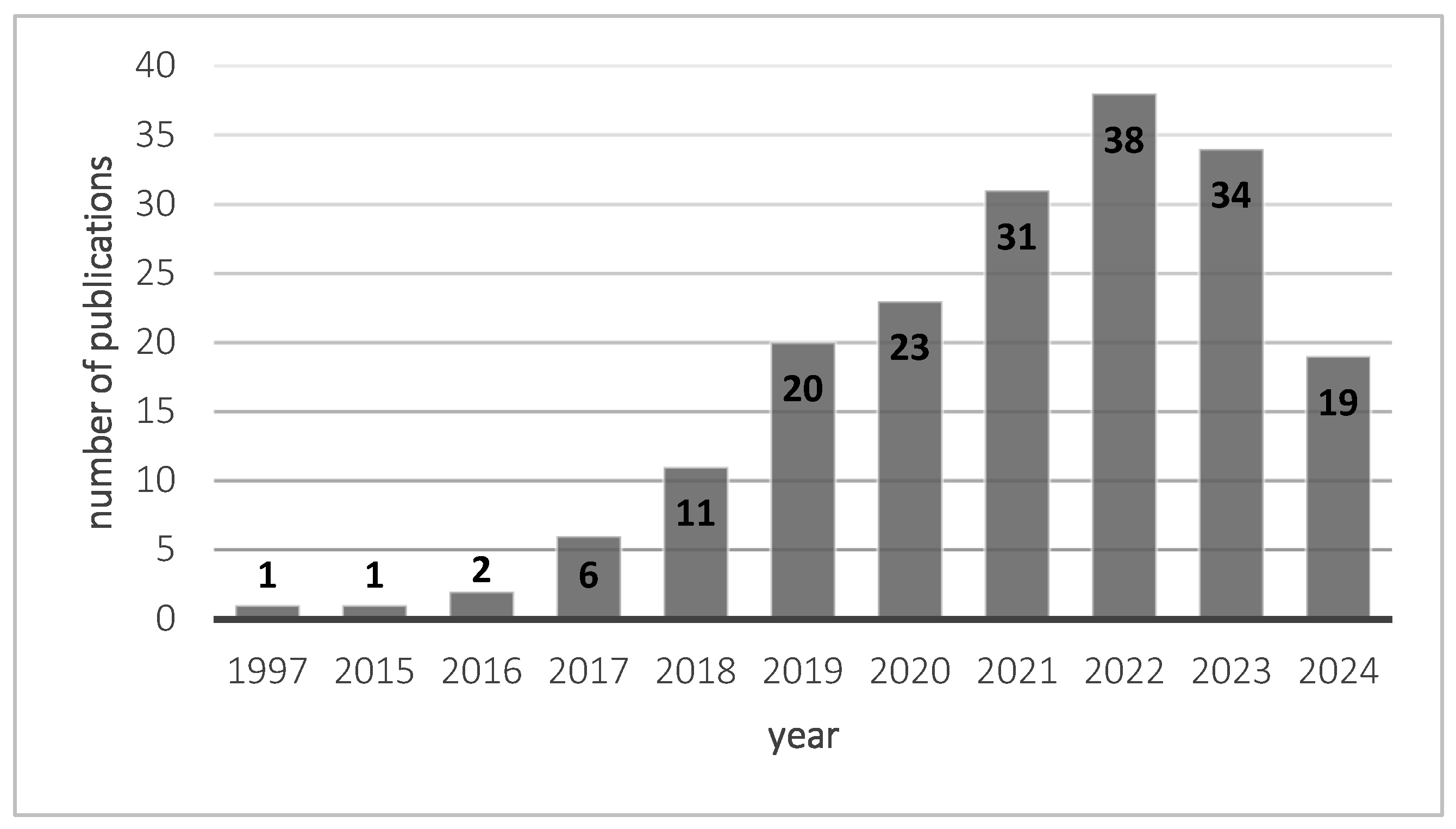
The electronics world is keeping an eye on 4D printing’s advancement, not only for actuator fabrication but also for sensor fabrication, using stimuli-responsive materials and self-healing structures obtained by combining printing technologies and materials [8]. However, 4D printing is still a relatively new and emerging technology; for this reason, the literature is pretty recent, with important growth in recent years (Figure 2).
The aim of this review is to give an insight into what has been achieved with 3D- and 4D-printing technologies in electronics, organizing the discussion as follows. Section 2 presents the printing technologies used to fabricate electronic devices, reporting some examples. Section 3 covers the materials used for 4D printing, together with some applications. Finally, Section 4 reports conclusions about the topic.

2. Printing Technologies

As seen in Table 1, different AM processes are employed for 4D-printing stimuli-responsive devices. Here, such technologies are reported, highlighting their potential applications.

2.1. Vat Photopolymerization-Based 4D Printing

AM technologies, like vat photopolymerization (VPP), were introduced in the context of 4D printing for electronics and robotics applications. Vat photopolymerization refers to different AM technologies, such as stereolithography (SL) and digital light projection (DLP). Layer by layer, the resin contained in a vat is photopolymerized with a laser or a projector, usually in the ultraviolet (UV)/near-UV or visible light regions. The printed object grows on a building platform that moves along the z axis in a bottom-up or top-down configuration. Among the other 4D-printing technologies, these systems usually ensure the highest level of resolution and accuracy, good layer adhesion, and good surface quality. They can print several pieces at the same time, depending on the building plate dimensions. The printing time is highly dependent on the printing parameters and the fabricated geometries [7,12].
Among VPP technologies, DLP is commonly spread in different fields nowadays, from jewellery to electronics, because it is able to print small devices (maximum printable sizes range from 100 × 60 mm2 to 190 × 120 mm2) with high precision and a high printing resolution, typically around 50 μm as a minimum lateral feature size. These outstanding properties are linked to the projector, which contains the DLP chip. This chip is an advanced optical switching device that is made of two million regular arrays of tiny microscopes working together [13]. The following example shows the application of DLP for the 4D printing of electronics.
  • Functional electronics
The group of Guo et al. [14] fabricated 3D electronics starting from a DLP-printed element and liquid metal coating on top. The aim of the work was to obtain functional electronics with flexible and stretchable structures that can reply to thermal stimuli. The main structure was made using the CL-60 HALOT-1 from Creality 3D Technology Co. Ltd. (Shenzhen, China) as a printer, which can print geometries with a resolution of 50 μm. The polymeric printed structure presented micro roughness on the surfaces, which could entrap air in the gaps. For this reason, they used polymethacrylates (PMAs) glue as pre-coating, dipping the 3D-printed structures inside it. After that, they coated the surface with a conductive liquid metal made of oxidized-eutectic alloy of Gallium and Indium (O-EGaIn). They evaluated the wettability of the coated devices, namely, the coating adhesive force, and found the optimized protocol to coat the structures. Such a protocol improved the coating selectivity to obtain well-defined conductive paths on the surface. In this way, they were able to fabricate reticular O-EGaIn patterns, as in Figure 3, that acted as conductive wires for the electronic components. Furthermore, the electrical performances of the patterns were studied to assess if they could serve as functional devices alone. They observed that the liquid coating could form bridges between two adjacent covered printed structures, improving mechanical performances and conductive patterns, which were easily reconfigurable. Lastly, they used a stretchable polymeric structure made of Ecoflex 00–30 from Smooth-On (Macungie, PA, USA) to evaluate the thermomechanical response of the coating. They found that the structures could support weights at low temperatures, while they collapsed under pressure at higher temperatures, due to the phase-change transition of the metal alloy. For this reason, this coating could be used as a network for the joints of rigid robots [14].

2.2. Material Extrusion-Based 4D Printing

Extrusion-based AM technologies are widely used today because of their simple set-up and lower equipment and energy costs compared to other processes like VPP. These fabrication techniques rely on a feedstock material extruded by a printing head using different extrusion strategies to obtain a viscous flow through the nozzle. After the deposition, two main approaches are employed to ensure the adhesion of each layer to the previous one. The first approach uses temperature changes to guarantee bond formation through the initial melting and the following solidification. The second one exploits a chemical curing to ensure the layers bonding, using curing agents inside the material that react with air, or with UV light or microwave radiation [15].
Nowadays, the most common diffused material extrusion technology is fused filament fabrication (FFF), also known as fused deposition modelling (FDM), from Stratasys, which enables object fabrication by extruding a molten filament from a heated needle. This technology is widely used, even if it has some drawbacks, such as low resolution because of the filament diameter. Other disadvantages are its low surface quality, bad surface finishing, and long printing time for complex objects [7]. However, such a 3D-printing technique has been introduced in the 4D-printing fabrication of electronic devices due to its low costs and easy manufacturing of parts.
Other extrusion-based AM technologies rely on liquid ink deposition through a nozzle that can be piezoelectrically or thermally activated. The material is stocked inside a tank or a syringe, and it is delivered to the nozzle of the printing head through a transmission line. The generated drops are deposited on a substrate, which can be flexible or rigid, heated or not, following a CAD-defined pattern. The deposition head can move along the x axis, and the building substrate can move along the z axis, while the Y axis deposition can be determined by the displacements of the head on the plane. If there are more nozzles, their position along the axis and their consequent activation determines the y axis positioning. After that, the material is cured with a lamp, with a wavelength of light between 190 nm and 400 nm [16]. These AM technologies can ensure thin layer thickness, thin wall features, good surface quality, and high resolution. However, especially with direct ink writing (DIW), great attention should be taken to the ink formulations since the chemical composition strongly affects the quality of the printed features, for example, with the coffee ring effect (CRE) [17].
  • Antennas
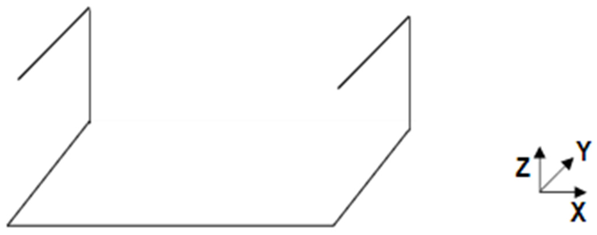
The first example of FFF application in electronic devices is presented in the work of Le et al. [18], who printed a free-standing 3D Hilbert dipole antenna using a commercial 3D printer (System 30, from Hyrel 3D, Norcross, GA, USA) with a homemade polyurethane (PU)-based electrically conductive adhesive (ECA). To obtain a self-standing structure, the ECA material was printed into a PDMS resin bath. The printed antenna was composed of fractal curves, as shown in Figure 4, since this shape ensured a better Q factor at the 433 MHz band. The first printed element was the planar part; the vertical ones were fabricated subsequentially. This antenna design included the Koch antenna, and it could be used for wireless wearable communication in on-body sensor network (BSN) applications [18].
Another example of a 3D-printed antenna is shown in the work of Cuevas et al. [19]. They fabricated a 5.8 GHz hemispherical dielectric resonator antenna (DRA) loaded with a metallic cap for vehicle-to-vehicle communication. They used a custom-made FFF 3D printer from Ocular3D (Viña del mar, Valparaíso, Chile) with two extrusion heads, one for the dielectric material (PREPERM ABS1000) and the other for the conductive material (Electrifi Multi3D, Cary, NC, USA). They analysed two different topologies that differ in the infill percentage of the two parts of the antenna’s main body. This difference implied a variation in the structure’s relative permittivity, which was compensated with metallic caps placed on top of the antenna bodies. The fabricated antennas showed a slight frequency shift of their resonance frequency, caused by the permittivity variation and the uncertainty on the permittivity of the conductive filament. The shift was also influenced by the fabrication tolerance of the printing technology. However, the resonance frequency was measured as 5.9 GHz, and the maximum gain varied from 3.8 dB to 4.7 dB, which is not so far from the theoretical prediction, even if some losses were introduced by the filaments. Lastly, they achieved a 22% weight reduction in the structure, which was beneficial in some applications, such as unmanned aerial vehicles (UAVs), where size and weight are considered crucial parameters in the device design [19].
A third example of an FFF-printed antenna is reported in the work by Sun et al. [20]. They fabricated a millimetre-wave dual-polarized dielectric resonator (DR) reflectarray (Figure 5) using the Creator Pro Flashforge 3D printer (Jinhua, China) with PREPERM 3-D ABS DK 10.0 filament from Premix (Rajamäki, Finland). The dual polarization was obtained through a well-defined geometrical configuration design of the DRs. They were made of two orthogonally positioned elliptical resonators, which ensured high isolation and independence between the two polarization directions. The antenna was made of 256 elements, and the working range was from 30 GHz to 40 GHz. Comparing the AM-fabricated antenna with traditional fabricated ones, they observed that their method allowed them to expand the substrate thickness, reducing costs and losses in high-frequency applications and implementing complex element shapes. Furthermore, the combination of the FFF technology with high relative permittivity materials helped them to obtain a reflectarray antenna with a low profile, a medium aperture efficiency, and dual polarization. The antenna could be easily tuned, and its peak gain was 22.53 dB in the range of 30 GHz–40 GHz [20].
FFF printing of antennas should be performed while considering that printing parameters can deeply affect the resultant relative permittivity value of the final objects, together with the material electrical parameters, as Tokan et al. [21] investigated. They studied the influence of parameters using a sample of Preperm ABS1000 from Premix and printing it with a core XY-type printer. By measuring the electrical characteristics of the printed samples, they observed that printing settings were crucial to obtaining the desired dielectric behaviour with high permittivity and low-loss thermoplastic material. In fact, FFF-fabricated antennas showed performances comparable with the traditionally fabricated ones only using the optimized set of printing parameters [21].
  • Self-morphing circuits
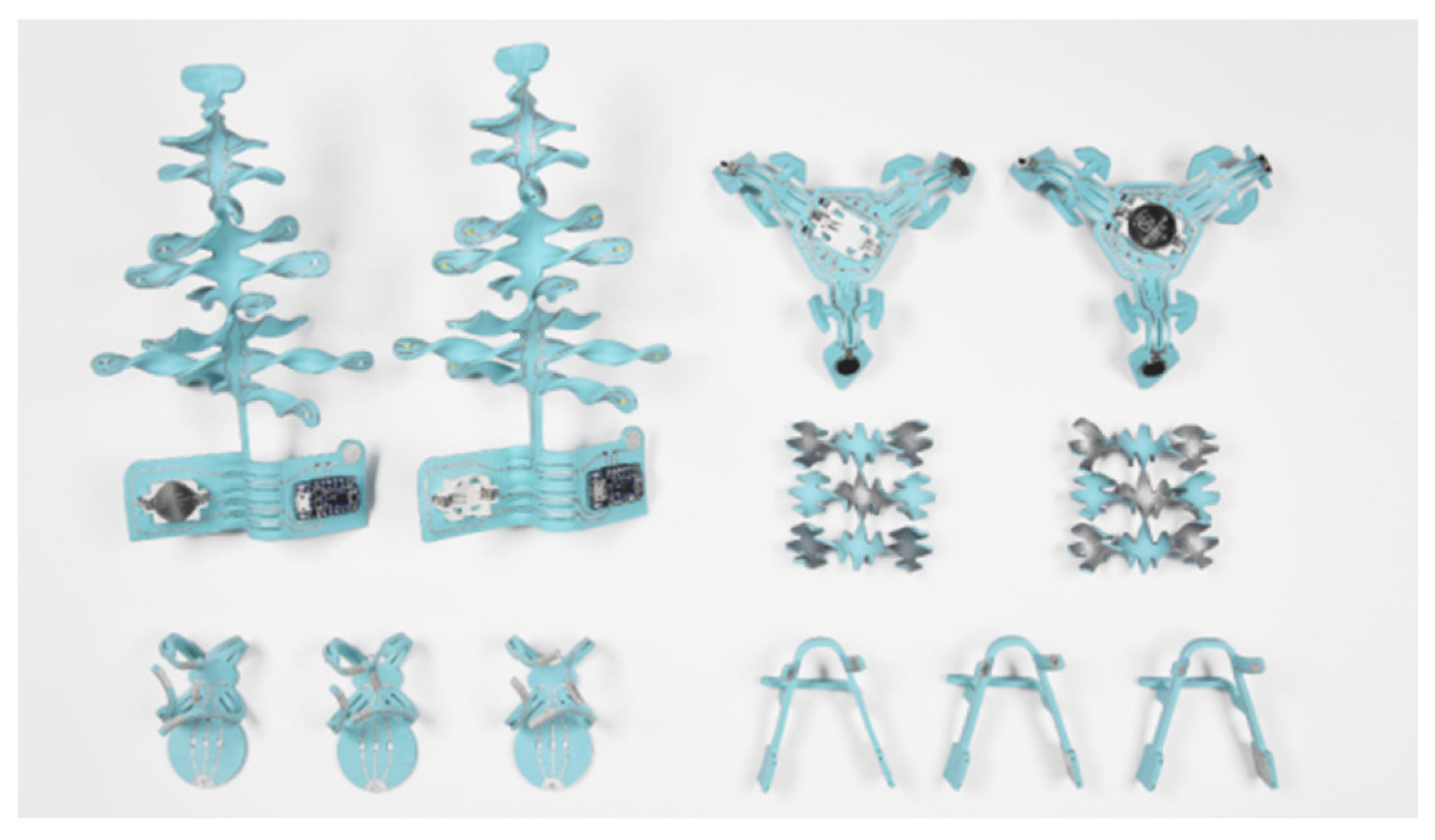
FFF technology has been applied not only for antennas but also for the fabrication of 3D self-folding electronics: morphing circuits that can change their 3D shape arrangements under an external stimulus. The work of Wang et al. is pioneering in this sense [22], as they presented a novel approach to this manufacturing process, highly detailed in their article. The process showed different advantages, such as lower costs, flexibility for accomplishing complex curvilinear surfaces, and applicability in even complex 3D structures. They started the multi-step process flow considering that the FFF manufacturing of thermoplastic materials causes shrinkage of the final printed parts when triggered by an external heating element due to residual stresses incorporated during the extrusion step. Firstly, the design of the printed electronics started with the 3D modelling of the substrate, which allowed them to extract the stresses in the object and which was then used for the morphing simulation through finite element analysis (FEA) software. They also simulated the addition of silver traces, surface-mounted device (SMD) insertion, and the thermal trigger influence on the morphing behaviour. After the validation of the design through simulation, the designed substrate was fabricated using a standard FFF machine, the MakerBot Replicator 2X (New York, NY, USA), with PloyMax PLA (Polymaker, Changshu City, China). They designed the substrate with holes and integrated sinks for the positioning of other components. Subsequently, they printed traces using the screen-printing technique, selecting the commercial silver ink CI-1001 from Engineered Materials Systems (Delaware, OH, USA) and the pre-coated screen HiDef stencils from EZ Screen (Washington, DC, USA). They selected this technology due to its simplicity, speed, and versatility across materials. In particular, they chose silver ink for its flexibility, water resistance, and low curing temperature, even if further improvements could be made to introduce more flexible materials, which could ensure better compliance with the morphing process. Lastly, they introduced the electronic components inside the designed accommodation and added the silver ink where necessary to connect traces and components. They verified the trigger response using two methods, namely, a hot water and oven, both at 90 °C, to understand if any different shapes or conditions appeared. They only evaluated bending, twisting, and coiling deformations, but the obtained results seemed to be promising to develop more complex structures with fewer geometric constraints, ensuring a low-cost and low-pollution solution for conformable electronics. In Figure 6, some examples of printed conformable electronics [22] are reported.
The literature example above shows that there is a strict correlation between all the five elements of 4D printing [8], highlighting the need for mathematical modelling and FEA simulations to properly design a self-morphing circuit. As stressed by Pei et al. [23], mathematical modelling is a fundamental step that allows producers to obtain the necessary time and sequence of stimuli to apply while considering the materials used, as well as their orientation and the expansion or contraction rate that the stimulus determines. This fabrication stage is usually characterized by the combination of FEA software with CAD ones [23], as in the self-folding structure of Wang et al. [22].
  • Sensors
A first example of extrusion-based AM technologies applied for sensor 4D printing is the work of Wan et al. [24], where they used DIW of a poly (D, L-lactide-co-trimethylene carbonate) (PLMC)/carbon nanotube (CNT) composite to fabricate a shape-changing liquid sensor. They selected this ink because of the shape-memory characteristic of PLMC and the electrical conductivity of CNT. These properties allowed them to obtain a shape-changing structure that could be programmed using an electrical field, adaptable to the target environment (Figure 7). Their ink was composed of crosslinking-PLMC, obtained by the dilution of Isopropylthioxanthone/1,2-Dibromoethane/PLMC/Dichloromethane (ITX/EDB/PLMC/DCM) with a weight ratio of 0.01:0.03:1:20 and 10% wt. of CNT. This solution was 3D-printed using a 3 mL syringe with a micronozzle, moved by a robot (I&J2200-4, from Fisnar, Germantown, MD, USA) that controlled the applied pressure (from 1.75 to 3.5 MPa) and speed. The printed structure was U-shaped, and it was tested using an immersion/drying cycle to record the electrical resistivity variation in real time. They observed that the so-prepared ink ensured good viscosity and enough fast evaporation, suitable for DIW fabrication. The electrical-responsive behaviour was strongly dependent on the CNT content because the electrical conductivity decreased with the decrease in the CNT concentration. They investigated the sensing performances of the printed device using different solvents and real-time monitoring of changes in resistivity. The sensor sensitivity was related to the polymer swelling during the immersion phase, which determined the disruption of the CNT network connections and a resistivity increase: when the volume of the wet sensor decreased, caused by a decrease in the liquid level, the sensitivity decreased with it. To overcome this problem, they changed the sensor shape through the external electrical field. This modification allowed them to evaluate the sensor in different environmental conditions and at lower liquid levels. In this way, the sensing abilities remained the same, even when folding the structure through the electrical field, which demonstrated good sensitivity. This combination of shape-changing behaviour with the conductivity characteristics of CNT could be of great interest for the liquid detection of several solvents in different conditions through a customized sensor, e.g., for environment monitoring [24].
Environment-monitoring sensors were also fabricated using extrusion-based AM technologies in the work of Ahmad et al. [25]. They proposed DIW and electrohydrodynamics (EHD) to make a flexible strain sensor, a temperature sensor, and a humidity one. EHD is an evolution of inkjet-printing technology: it relies on the dropwise deposition of a liquid ink under the influence of a strong electric field that induces the formation of the drops in the extrusion capillary, determining the arrangement of the ink particles on the printing substrate, as explained in Figure 8 [26].
The optimization of EHD printing parameters and ink characteristics, like viscosity, results in a high printing quality, high resolution, and stable and reproducible results.
In [25], the resistive strain and the flexible sensors were produced by DIW with a carbon paste. The latter was deposited on a poly (ethylene terephthalate) (PET) substrate and showed a gauge factor of 59 and a high control on the pattern width, which was measured to be less than 250 μm. Sensors’ resistance varied with the temperature and humidity oppositely. Meanwhile, the humidity sensor and the resistive temperature sensor were printed using EHD. Silver nanoparticle ink was deposited on the PET substrate; then, the whole object was tested to verify the temperature coefficient of resistance, which was 8.41, and the sensitivity to humidity level, which was observed to be very high. Furthermore, to obtain the humidity sensor, a Poly(3,4-ethylenedioxythiophene): poly(3,4-ethylenedioxythiophene)-poly(styrene sulfonate) (PEDOT:PSS) ink was deposited on silver electrodes, which were fabricated on top of a paper substrate. The so-fabricated device showed a good response with a low recovery time, an operating range from 40% to 100% relative humidity, and capacitance and resistance changes of 4.22 pF and 4.69 MΩ, respectively. Even if these environmentally friendly devices were very promising, they still need improvement. Further investigations should be performed to enhance sensor performance in environmental monitoring and other applications [25].

2.3. Multi-Method Fabrication Solutions

As shown in the previous paragraph, there is a growing trend in the combination of different AM technologies of the same category or of different families. An example is the work of Roach et al. [27], which combined four fabrication techniques (inkjet printing, DIW, FFF, and aerosol jetting) with a pick-and-place (PnP) robotic arm and photonic curing for intense pulsed light (IPL) sintering to make a multi-material soft pneumatic actuator and a multi-material stretchable electronic device for many applications, which range from wearables to aerospace.
While DIW and FFF printing have already been presented in the previous paragraphs, inkjet printing (IJP) and aerosol jetting (AJ) will be presented hereinafter. Both technologies belong to the extrusion-based AM technologies world, but they differ in the ink-deposition method. In IJP, liquid ink is ejected dropwise through the nozzle, which is part of a piezoelectric MEMS actuator. The printing process is voltage-controlled, with the pneumatic ejection of drops on demand. IJP shows high accuracy and resolution, even if the deadtime between drops can cause nozzle clogging [28]. In AJ, the liquid ink is atomized through a pneumatic or ultrasonic atomizer first. Then, the dense, tiny drops are transported to the deposition head using a nitrogen carrier gas. The gas helps the collimation of the ink flow into the deposition head, which ejects the drops with a high velocity, allowing them to travel 2–5 mm from the nozzle. The deposition system is usually a 5-axes system that also enables the printing of low-viscosity (under 1000 cP) inks on hydrophilic 3D substrates [29]. Even if this technology has some limitations, due to the restricted number of commercial solutions available, it presents some advantages, such as ink versatility, a non-contact printing phase, a micrometric 3D structure fabrication (under 50 μm), fast printing processes, and high reproducibility [30].
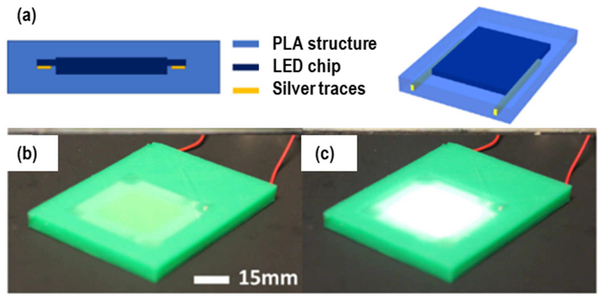
Getting back to [27], a complex multi-technology platform was developed, with seven printheads: two FFF heads from Prusa3D; two DIW pneumatic syringes controllers UltimusV from Nordson EFD; two IJP piezoelectric drop-on-demand modules Xaar 1003 from Xaar Plc; and one AJ module AJ 5X System from Optomec Inc, Albuquerque, United States of America. The curing was carried out by an FE300 UV LED lamp from Phoseon for IJP and an RC-847 Xenon Corp flash lamp for photonic curing. Finally, two robotic manipulators for PnP, a six-axis robotic manipulator (C4 from Epson Inc.) and a four-axis robotic manipulator (G3 from Epson Inc., Suwa, Nagano, Japan), were included in the equipment. This complex printing system was coupled with a five-motion printing bed, made of one X- Y-motion stage and four Z-motion stage, from Aerotech Inc. A common communication language between the several technologies had to be developed because each AM technology relied on different programming languages and independent coordinate systems. Firstly, kinematic transformations to the printing coordinates were applied; then, a highly complex algorithm was coded in Python with a user-friendly interface. This interface allowed the users to insert the G-Code for FFF or DIW, select the printing technology, set the printing parameters, and obtain a final file that the motion stage can use for the object’s fabrication. The printing platform offered flexibility in both printing methods and materials, allowing for the integration of diverse functionalities within a single component. Some examples of functionality integration were presented in [27]. The first example is a soft pneumatic actuator for soft robotic applications. It was composed of two layers: a top extensible layer fabricated through DIW using an elastomer, and a bottom flexible, inextensible one of a rigid photopolymer fabricated with IJP. Some hollow chambers were designed between the two layers, made accessible thanks to an inlet hole that could be pressurized to bend the structure. The inlet hole was used to insert a nozzle connected to a pressure switch; activation caused the inextensible material to bend as the bottom layer expanded. When the switch was turned off, the structure recovered its initial structure. Another example presented in [27] was the fabrication of a digital LED lamp, whose base structure was 3D-printed through FFF printing of PLA. The LED chip was then picked and placed in the designed housing by the six-axis robotic arm. Lastly, conductive silver ink was deposited into the channels through DIW, which were cured using the photonic module, forming the connection traces for the external power supply. The chip and traces were encapsulated with the FFF printing of PLA. The final printed LED light is reported in Figure 9. Although this complex system showed good performance and several advantages, like the possibility of working on the same component with different materials, some challenges seemed to be addressed. As a matter of fact, by using different techniques, differences in resolution appeared, and the feature resolution was deeply influenced by the lowest one. Therefore, some methodologies and solutions should be adopted to overcome this problem, like increasing the number of deposited layers in the technologies with thinner layer thickness, in order to obtain results that could be compared to the technologies with a thicker layer thickness. Another problem to address was the deposition of conductive ink on rough surfaces because these inks tended to fill voids and cracks on the surfaces, decreasing the trace conductivity, so thicker ink layers had to be deposited to avoid this reduction in conductivity values.
The thesis of Peng [31] is the combination of more than one AM technology to obtain a 4D-printed structure, where a hybrid fabrication process was used for prototyping a liquid crystal elastomer (LCE)-based actuator for soft robotics. In particular, the presented set up combined digital light processing (DLP) of a support structure with laser-assisted DIW of LCEs. The in situ laser curing of LCE-based polymers ensured the rapid fixing of the shape and alignment, while the DLP-fabrication step provided the freedom of fabrication and the design for supporting structures. To prevent any impact from the laser on the DLP resin, the LCE ink should cure rapidly, and the selected photoinitiator should work in a different wavelength range. After the preparation of the two compositions, the printing phase involved a two-step process: first, the DLP fabrication of the support structure, then, its placing in the laser-assisted DIW position using the Z-moving building platform and the X- and Y-moving DIW printing head. The head also allowed the alignment of the fibres into the ink, guaranteeing a freestanding, stable structure. The actuation behaviour of the printed LCEs was evaluated through finite element analysis (FEA) simulation, and the empirical test results were in line with the FEA ones. They found that the printed LCEs lattice had a controllable shrinkage through temperature variations; they could be considered tensegrity structures, with compressive stiff elements and tensional wires, which were relaxed at room temperature and tightened up when heated. These characteristics gave the ability to obtain an actuator with a tuneable structural stability that varies with the temperature and whose active parts could also be fabricated and actuated in a 3D space using DLP materials to print removable supports [31].
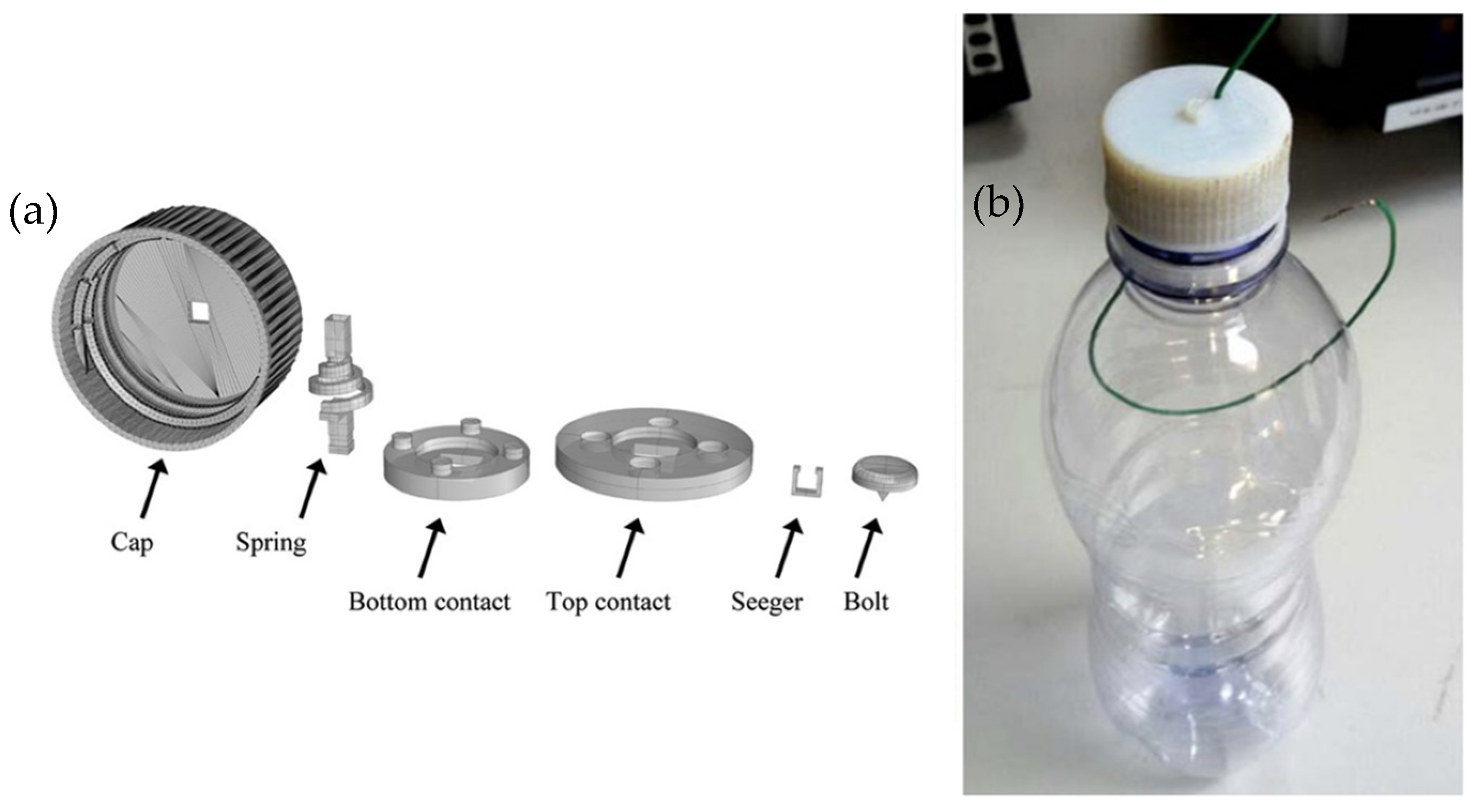
A third example of multi-method fabrication solutions for the AM of electronic devices is reported in the work of Marasso et al. [32]. They described a smart cap for plastic bottles that detected the open/close positions and the temperature of the cap through the integration of several additive manufactured elements. Firstly, they evaluated the resistivity of the electrically conductive material used for the device, which was a conductive PLA filament from Protoplant INC. For this purpose, they printed a 10 × 10 × 10 mm3 cube using an FFF printer (K8200 from Velleman, Gavere, Belgium) with the following parameters: 60% infill density with honeycomb rectilinear pattern, 225 °C and 55 °C nozzle temperature and bed temperature, respectively, and 65 mm/s infill speed. Then, they deposited a thin film of Ti/Al on four sides of the structure through sputtering (Kurt Lesker PVD 75) to obtain contact pads for wires. After the resistivity measurements, they designed and fabricated the smart cap in Figure 10 below, selecting FFF technology for printing the contacts with the tested PLA. The other components were 3D-printed through PolyJet technology using VeroWhite Plus FullCure 835 as constitutive material and Object 30 as a printer, both from Stratasys (Eden Prairie, MN, USA).
PolyJet technology was developed by Objet Geometries Ltd. (Rehovot, Israel) in 2000, now part of Stratasys, and it combines material deposition with its photopolymerization with a UV light [33]. Two materials are deposited on the building platform by two inkjet print heads; one is the support material, while the other one is the model material. They are deposited layer by layer with a thickness of 16 µm, then spread with a roller, and, lastly, cured by a UV lamp. At the end of the process, the printed objects should be post-processed to eliminate the support material and to ensure the finalization of the photopolymerization process with a thermal treatment, especially if the parts are used as moulds [34,35]. The resolution of this technology is 656 × 656 × 1600 DPI (XYZ) [36], and the accuracy is 0.1 mm [33].
In [32], the printed smart cap exhibited a significant resistance variation during open/close tests, along with changes in temperature, demonstrating the potential of applying AM technologies in packaging to monitor changes in stored goods without the need to open them.
In the following Table 2, all the mentioned examples are summarized, divided by application.

3. Smart Materials

The main advantage of 4D printing over 3D printing is the capacity to develop a system that can smartly evolve over time [8]. The reason for this time-evolution capability can be found in the materials used. Indeed, they are generally defined as smart materials (SM) because of their ability to modify their characteristics in response to a specific stimulus [37]. There are numerous stimuli that can be exploited to trigger the change. Temperature is the most employed stimulus in 4D-printing structures because the vast majority of SMs used for this technology exhibit a transitional temperature, Ttrans, which generally refers to the melting temperature or the glass transition temperature. As the Ttrans name suggests, these responsive materials can modify themselves in accordance with a temperature gradient. Another stimulus that is broadly investigated in electronics is the electric stimulus: electric fields are employed as an indirect stimulus to create heating effects and to trigger materials that present a Ttrans. Equivalently, magnetic fields can be used when magnetic materials are employed. Light can also be adopted as a stimulus: in this case, the observed morphing is a consequence of photon energy exchange with functional groups present in the material. As a result, alterations are made to the binding interaction, leading to temporary physical or chemical crosslinks. Other stimuli employed in literature are pH and moisture, mostly used for polymers or hydrogels [38].
Similarly, several modifications can be triggered in the material, including changes in colour [39,40], electronic properties [41], or self-healing mechanisms [42]. However, among various types of SMs, the materials characterized by a shape-change behaviour, namely, shape memory materials (SMMs), show a particular suitability for AM technologies [43].
SMMs can be divided into two distinct categories depending on the shape change mechanism. The first category includes the so-called shape-memory effect (SME), which occurs when the material can recover its original shape after a quasi-plastic deformation. The second group covers the shape-change effect (SCE). In this case, the magnitude of the shape modification is proportional to the intensity of the applied stimulus, and it disappears when the trigger stops [44]. However, it should be considered that both mechanisms can be found in the same material. For instance, a hydrogel undergoes swelling or shrinking depending upon wetting or drying, which is an SCE, but shape recovery may also be induced, triggering an SME concurrently. Therefore, the hydrogel can be classified as a shape-changing material or a shape memory material, depending on the environment or working conditions.
Typically, a full SME cycle is composed of two processes: programming and recovery [45,46]. During the first phase, a temporary shape is programmed while the stimulus is applied; subsequently, the external stimulus triggers the material to recover to its permanent shape during the second phase. Thus, 4D printing is advantageous in this case since it permits programming complex shapes, even in composite structures [47]. Moreover, SMMs can be classified as one- or multiple-way materials, depending on the number of shape alterations they undergo. In one instance, the initial shape cannot be recovered, whereas in all other cases, it is regained as a temporary shape.
Several types of materials have been investigated in 3D- and 4D-printing processes, such as shape memory polymers (SMPs) and elastomers [48], hydrogels and aerogels [37], shape memory alloys (SMAs) [49], shape memory ceramics (SMCs) [50,51], composites, and nanomaterials [52,53], showing the great potential of this technology.

3.1. Polymers and Composites

The vast majority of studies on 4D-printed electronics rely on SMPs due to the variety of stimuli they can undergo and their suitability for printing processes [54]. As a matter of fact, they have been adopted in many applications, such as sensors [55,56,57], actuators [58,59], and wearable electronics [60,61,62].
Polymeric composites, specifically, have been deeply investigated in the field of 4D-printed electronics in order to combine the flexibility given by a polymeric matrix with other properties, such as higher conductivity given by the filler material [24,63]. Indeed, multifunctional materials are fundamental to producing adaptable and autonomous devices.
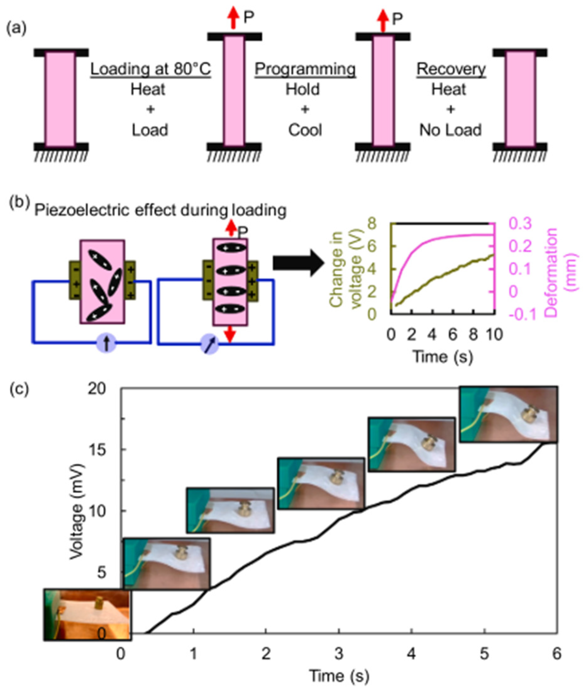
An example of the potential of composites in this field is shown by Bodkhe and Ermanni, who merged piezoelectricity with shape-memory behaviour [64]. In this work, a polymeric blend composed of poly-lactic acid (PLA) and poly-ester amide (PEA) in a 20:80 ratio was filled with barium titanate nanoparticles to produce an ink with piezoelectric behaviour. The ink was then employed to print structures with different geometries via DIW. In this case, the structure was exploiting the SME, showing a permanent shape and a deformed one with the Tg as Ttrans at 80 °C. The second configuration was reached by heating the sample above the Ttrans while stretching it with a given force and then cooling it down, maintaining the stressed state to fix the shape (Figure 11a). The piezoelectric effect was detectable in the stressed configuration: when the sample was deformed again after the programming, the piezoelectric voltage output was detected (Figure 11b). Figure 11c shows the final demonstrator, which is beam-shaped: the electrodes were placed on both sides of the beam, and the temperature was gradually increased up to 100 °C, while a 2g load was also applied to fasten the deformation process. As can be seen in the graph, the voltage was proportional to the deformation. The result was a sensor capable of withstanding a broad range of temperatures, from 23 °C to 100 °C over 5000 operation cycles.
Another example of smart composites can be found in the work of Wu et al. [65]. In their study, nylon was embedded and extruded with carbon fibre to exploit the significant difference between the thermal expansion coefficients of the two materials, thus achieving a thermotropic deformation. Here, the shape-changing mechanism relied on the SCE because the deformation of the printed substrate was dependent on the environmental temperature: the bending angle was more accentuated for lower temperatures. When a voltage was applied to the carbon fibre, the local temperature slowly increased, resulting in a complete stretching of the substrate. The smart substrate was used to control the beamwidth and gain of a bowtie antenna, which could provide a wide frequency range and radiation characteristics useful in many applications, such as 5G applications or wearable electronics.
Moving to a different application, Chen et al. presented an integrated strain and temperature self-sensing sensor–actuator [66]. They formulated a composite based on carbon black, providing high conductivity, and polylactic acid, which exhibits good shape-memory behaviour based on SCE. The material was 4D-printed using FDM technology to convey a gradient bioinspired gap. The structure was sensitive to strain due to the drop in resistance resulting from mechanical deformation and the closure of the gaps, which allowed a tunnelling current among carbon black nanoparticles. Moreover, it also showed a temperature sensitivity of 1.90–2.25 × 10⁴ ppm °C−1, given by a variation in the electrical resistance. The printed structure had the capability to touch objects in an active way and obtain feedback through the resistance signal, thus forming the active perception ability.
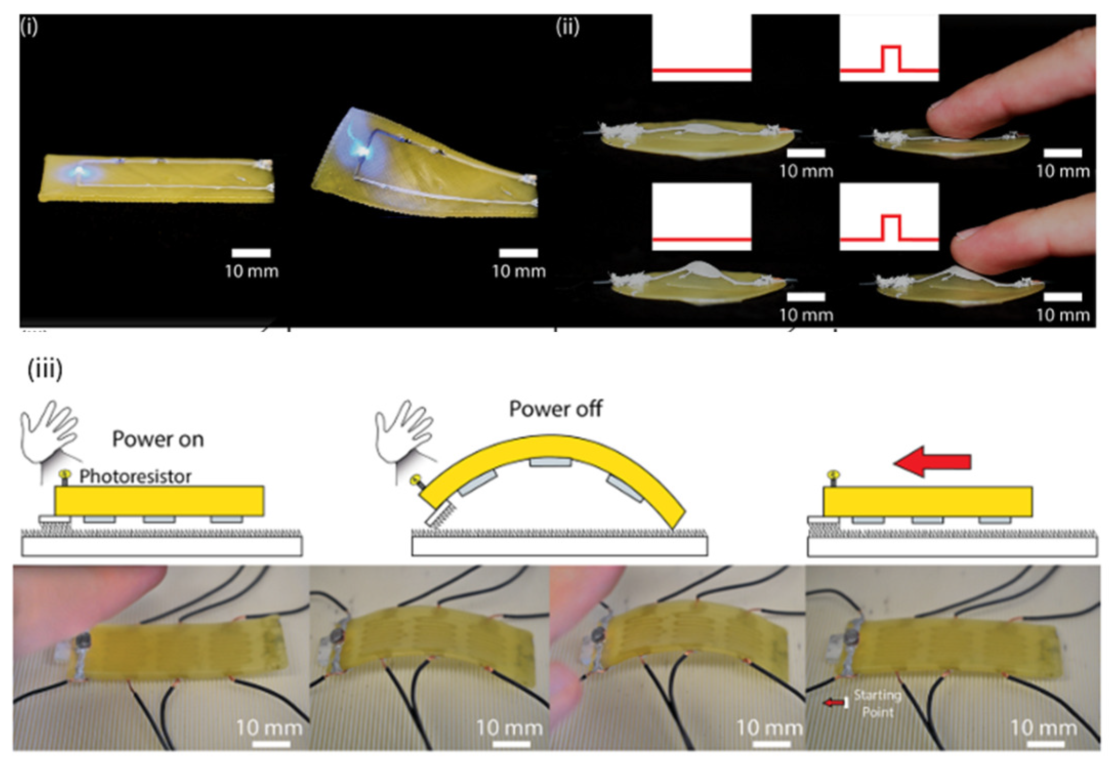
Finally, an interesting approach is presented by Vinciguerra and coworkers, which combined liquid metals (LM), namely, eutectic gallium–indium alloy, with liquid crystal elastomer (LCE) to obtain an electrically responsive system [67]. Both the materials were processed using DIW technology: the LCE was printed to form the substrate shape first, and then the LM ink was patterned on top to function as circuit wire and all the other electrical components. The outcome was a completely flexible and shape-reconfigurable structure suitable for many applications, such as a twisting actuator or a capacitive touch sensor. The deformation mechanism can be attributed to the SCE in this study as well (Figure 12).

3.2. Metal Alloys and Ceramics

The shape-memory effect in SMAs is based on the temperature-triggered phase transformation between a deformed state, namely, the martensitic phase, and a relaxed one, called the austenitic phase. This transition is the cause of the unique superelasticity. The great majority of SMAs are based on NiTi alloys, which ensured them great success in the biomedical industry due to their peculiar properties, including strength, good biocompatibility, and thermo-responsivity [68,69]. In addition, copper-based alloys for temperature-controlling systems [70] and other alloys [71] have been studied, even though they present stability and performance limitations. The potential of these alloys has been investigated for the electronic field in cooling systems [72,73,74], but also in radio frequency applications [75], vibration isolation [76,77,78], and actuators [79,80]. However, their presence in this field is not yet established, and 4D-printing technologies have not been explored in depth.
A few examples of 4D-printed components can be found in robotic devices. Yao et al. presented the development of a soft crawling bioinspired robot as an application case with two deformable structures [81]. Via laser powder bed fusion, they fabricated a monolithically deformable sheet as a body while a smart spring was manufactured and placed underneath to imitate the longitudinal muscles of an inchworm. In both cases, the alloy used was Nitinol, a Ni-Ti alloy known for its good shape memory strain of approximately 10%. The crawling movements were obtained by exploiting the non-equilibrium and equilibrium states between the two parts, which worked in an antagonistic way, being deformed in an alternating manner while a certain current was applied. The result demonstrated the potential advantage of developing a fully metallic structure that combines the flexibility of the shape-memory behaviour with the mechanical properties of a metal alloy, even if the printing method still needs to be improved.
A second example is the study by Aryaman et al.: they designed and fabricated a 4D-printed actuator for Flapping Wing Micro Aerial Vehicles (FWMAVs) [82]. As in the previous work, Nitinol was used in the form of wires that were embedded and printed in a thermoplastic elastomeric matrix of TPE-83A. The structure was able to recover its permanent shape after the application of a current that heats it above its Ttrans, inducing a mechanical deformation. The actuator presented a deflection range from −54° to 78° with respect to the 0 position. However, the fastest recovery time obtained was 17 s, which is still not sufficient for high-speed bending applications.
Smart ceramics present interesting, multidimensional properties driven by the materials’ fine particle size and their degree of aggregation. The mechanism of shape recovery is based on a temperature trigger again: when they are deformed beyond their elastic limit, they display a micro-deformation generated by external forces, which can be recovered through heat treatment. Metal oxide-based ceramics are the most commonly used in this field, except for ZrO2-based ceramics, which are widely employed because of their unique superelastic behaviour combined with a shape-memory response [83].
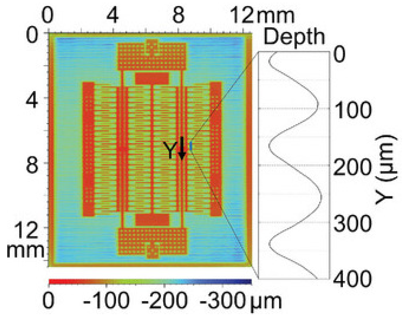
Smart ceramics are gaining ground in the field of smart electronics, with additive manufacturing technologies emerging as promising technologies for smart structure fabrication [50]. However, the design of the manufacturing processes and the definition of the printing parameters remain challenging [84]. Nonetheless, some attempts have been presented [85]. Here, we present a ceramic MEMS resonant strain sensor that is described in detail in Liu et al. work. The device was manufactured with a 4D additive–subtractive technique [86]: this process is based on the printing of an elastomeric ceramic precursor with DIW technology, which is subsequently laser-engraved to obtain a ceramic structure (Figure 13). With this method, the authors claimed that the strain sensitivity could be improved and the environmental interference decreased compared to a common resonant strain sensor.

4. Conclusions

This work explores the world of 3D- and 4D-printing techniques applied to electronic and soft robotics devices. As explained in the first section, the fabrication methodology is based on the combination of five factors: AM technologies, materials, stimuli, interactions, and models, all contributing to the desired results.
What emerges from our literature review is that different AM technologies were employed in different contexts, from sensor fabrication to morphing circuits, exploiting all their potential application fields and their compatibility with new materials. AM advantages facilitate the achievement of objectives, like a fast printing process, simple fabrication, low costs, tuneable polymer printing, versatility [61], fewer geometric constraints during the design phase, low-pollution solutions for electronics [22], and weight reduction of the structure, which could be beneficial to several application fields [19]. Moreover, the application of 4D printing with SMs opens doors to a deep exploration of wearable and soft electronics, where materials adapt and respond to environmental stimuli, unlocking further opportunities for innovation in such a field.
Nevertheless, further improvements should be made to enhance the performance of 4D-printed devices, especially for some currently relevant applications [25], and to integrate different technologies together for complex systems [27]. Furthermore, the research field of materials selection remains broadly open to the amelioration of printed material properties and processes; the integration of multi-stimuli structures; and further exploration of different materials, such as ceramics and alloys. Nonetheless, the combination of the analysed factors, along with the previously mentioned ones, has enabled the exploration of cutting-edge solutions for electronics, soft robotics, biomedicine, automotives, and aerospace for both present and future societies. At present, there are no commercially available electronic products that significantly exploit 3D or 4D printing due to the early stage of technological development. As a result, 3D- or 4D-printed electronics are predominantly found in research laboratories or as prototypes, considering that traditional electronics-fabrication processes remain easier, cheaper, and more reliable. However, as the research in this field continues to advance, the prospect of developing truly adaptive and autonomous devices appears increasingly feasible.

Author Contributions

Conceptualization, M.A. and M.P.; methodology, M.A. and M.P.; resources, M.A.; writing—original draft preparation, M.A. and M.P.; writing—review and editing, S.L.M., V.B. and F.F.; visualization, S.F. and L.S.; supervision, S.L.M. All authors have read and agreed to the published version of the manuscript.

Funding

This research received no external funding.

Acknowledgments

This study was carried out within the MICS (Made in Italy—Circular and Sustainable) Extended Partnership and received funding from the European Union Next-GenerationEU (NATIONAL RECOVERY AND RESILIENCE PLAN (NRRP)—MISSION 4 COMPONENT 2, INVESTMENT 1.3—D.D. 1551.11-10-2022, PE00000004). This publication is part of the project (NATIONAL RECOVERY AND RESILIENCE PLAN (NRRP)- European Union Next-GenerationEU, which has received funding from the Ministry of University and Research—Ministerial Decree 118/2023.

Conflicts of Interest

The authors declare no conflicts of interest.

References

  1. Tong, C. Advanced Materials for Printed Flexible Electronics, 1st ed.; Springer Cham: Bolingbrook, IL, USA, 2022; Volume 317. [Google Scholar] [CrossRef]
  2. Subramanian, V.; Chang, J.B.; de la Fuente Vornbrock, A.; Huang, D.C.; Jagannathan, L.; Liao, F.; Mattis, B.; Molesa, S.; Redinger, D.R.; Soltman, D.; et al. Printed Electronics for Low-Cost Electronic Systems: Technology Status and Application Development. In Proceedings of the ESSDERC 2008—38th European Solid-State Device Research Conference, Edinburgh, UK, 15–19 September 2008; IEEE: Piscataway, NJ, USA, 2008. [Google Scholar] [CrossRef]
  3. Bonnassieux, Y.; Brabec, C.J.; Cao, Y.; Carmichael, T.B.; Chabinyc, M.L.; Cheng, K.T.; Cho, G.; Chung, A.; Cobb, C.L.; Distler, A.; et al. The 2021 Flexible and Printed Electronics Roadmap. Flex. Print. Electron. 2021, 6, 023001. [Google Scholar] [CrossRef]
  4. ISO/TC 261; ASTM Committee F42; Technical Committee CEN/TC 438. ISO/ASTM 52900:2021(en) Additive manufacturing—General principles—Fundamentals and vocabulary. Available online: https://www.iso.org/obp/ui/#iso:std:iso-astm:52900:ed-2:v1:en (accessed on 30 May 2024).
  5. Khorasani, M.; Loy, J.; Ghasemi, A.H.; Sharabian, E.; Leary, M.; Mirafzal, H.; Cochrane, P.; Rolfe, B.; Gibson, I. A Review of Industry 4.0 and Additive Manufacturing Synergy. Rapid Prototyp. J. 2022, 28, 1462–1475. [Google Scholar] [CrossRef]
  6. Praveena, B.A.; Lokesh, N.; Buradi, A.; Santhosh, N.; Praveena, B.L.; Vignesh, R. A Comprehensive Review of Emerging Additive Manufacturing (3D Printing Technology): Methods, Materials, Applications, Challenges, Trends and Future Potential. Mater. Today Proc. 2022, 52, 1309–1313. [Google Scholar] [CrossRef]
  7. Alammar, A.; Kois, J.C.; Revilla-León, M.; Att, W. Additive Manufacturing Technologies: Current Status and Future Perspectives. J. Prosthodont. 2022, 31, 4–12. [Google Scholar] [CrossRef] [PubMed]
  8. Ahmed, A.; Arya, S.; Gupta, V.; Furukawa, H.; Khosla, A. 4D Printing: Fundamentals, Materials, Applications and Challenges. Polymer 2021, 228, 123926. [Google Scholar] [CrossRef]
  9. Momeni, F.; Hassani, M.; Liu, X.; Ni, J. A Review of 4D Printing. Mater. Des. 2017, 122, 42–79. [Google Scholar] [CrossRef]
  10. Chen, A.; Yin, R.; Cao, L.; Yuan, C.; Ding, H.K.; Zhang, W.J. Soft Robotics: Definition and Research Issues. In Proceedings of the 2017 24th International Conference on Mechatronics and Machine Vision in Practice (M2VIP), Auckland, New Zealand, 21–23 November 2017; IEEE: Piscataway, NJ, USA, 2017. [Google Scholar] [CrossRef]
  11. Wehner, M.; Truby, R.L.; Fitzgerald, D.J.; Mosadegh, B.; Whitesides, G.M.; Lewis, J.A.; Wood, R.J. An Integrated Design and Fabrication Strategy for Entirely Soft, Autonomous Robots. Nature 2016, 536, 451–455. [Google Scholar] [CrossRef] [PubMed]
  12. Truxova, V.; Safka, J.; Seidl, M.; Kovalenko, I.; Volesky, L.; Ackermann, M. Ceramic 3d Printing: Comparison of SLA and DLP Technologies. MM Sci. J. 2020, 2, 3905–3911. [Google Scholar] [CrossRef]
  13. Quan, H.; Zhang, T.; Xu, H.; Luo, S.; Nie, J.; Zhu, X. Photo-Curing 3D Printing Technique and Its Challenges. Bioact. Mater. 2020, 5, 110–115. [Google Scholar] [CrossRef]
  14. Guo, R.; Zhen, Y.; Huang, X.; Liu, J. Spatially Selective Adhesion Enabled Transfer Printing of Liquid Metal for 3D Electronic Circuits. Appl. Mater. Today 2021, 25, 101236. [Google Scholar] [CrossRef]
  15. Altıparmak, S.C.; Yardley, V.A.; Shi, Z.; Lin, J. Extrusion-Based Additive Manufacturing Technologies: State of the Art and Future Perspectives. J. Manuf. Process. 2022, 83, 607–636. [Google Scholar] [CrossRef]
  16. Gülcan, O.; Günaydın, K.; Tamer, A. The State of the Art of Material Jetting—A Critical Review. Polymers 2021, 13, 2829. [Google Scholar] [CrossRef] [PubMed]
  17. Marasso, S.L.; Cocuzza, M. (Eds.) High Resolution Manufacturing from 2D to 3D/4D Printing; Springer International Publishing: Cham, Switzerland, 2022. [Google Scholar] [CrossRef]
  18. Le, T.; Tuan, C.C.; Bahr, R.A.; Wong, C.P.; Tentzeris, M.M. A Novel Approach to Integrating 3D/4D Printing and Stretchable Conductive Adhesive Technologies for High Frequency Packaging Applications. In Proceedings of the Proceedings—Electronic Components and Technology Conference, Las Vegas, NV, USA, 31 May–3 June 2016; Institute of Electrical and Electronics Engineers Inc.: Piscataway, NJ, USA, 2016. [Google Scholar] [CrossRef]
  19. Cuevas, M.; Pizarro, F.; Leiva, A.; Hermosilla, G.; Yunge, D. Parametric Study of a Fully 3D-Printed Dielectric Resonator Antenna Loaded with a Metallic Cap. IEEE Access 2021, 9, 73771–73779. [Google Scholar] [CrossRef]
  20. Sun, Y.X.; Wu, D.; Ren, J. Millimeter-Wave Dual-Polarized Dielectric Resonator Reflectarray Fabricated by 3D Printing with High Relative Permittivity Material. IEEE Access 2021, 9, 103795–103803. [Google Scholar] [CrossRef]
  21. Tokan, F.; Demir, S.; Çalışkan, A. Influence of 3D Printing Process Parameters on the Radiation Characteristics of Dense Dielectric Lens Antennas. Prog. Electromagn. Res. C 2021, 116, 113–128. [Google Scholar] [CrossRef]
  22. Wang, G.; Qin, F.; Liu, H.; Tao, Y.; Zhang, Y.; Zhang, Y.J.; Yao, L. Morphingcircuit: An Integrated Design, Simulation, and Fabrication Workflow for Self-Morphing Electronics. In Proceedings of the ACM on Interactive, Mobile, Wearable and Ubiquitous Technologies; 2020; Volume 4. Available online: https://dl.acm.org/doi/10.1145/3432232 (accessed on 17 July 2024). [CrossRef]
  23. Pei, E.; Loh, G.H. Technological Considerations for 4D Printing: An Overview. Prog. Addit. Manuf. 2018, 3, 95–107. [Google Scholar] [CrossRef]
  24. Wan, X.; Zhang, F.; Liu, Y.; Leng, J. CNT-Based Electro-Responsive Shape Memory Functionalized 3D Printed Nanocomposites for Liquid Sensors. Carbon 2019, 155, 77–87. [Google Scholar] [CrossRef]
  25. Ahmad, S.; Shakeel, M.; Iqbal, N.; Amin, M.; Rahman, K. Printing of Low Cost Sensors by Additive Manufacturing. In Proceedings of the 18th International Bhurban Conference on Applied Sciences and Technologies, IBCAST 2021, Islamabad, Pakistan, 12–16 January 2021; Institute of Electrical and Electronics Engineers Inc.: Piscataway, NJ, USA, 2021. [Google Scholar] [CrossRef]
  26. Mkhize, N.; Bhaskaran, H. Electrohydrodynamic Jet Printing: Introductory Concepts and Considerations. Small Sci. 2022, 2, 2100073. [Google Scholar] [CrossRef]
  27. Roach, D.J.; Hamel, C.M.; Dunn, C.K.; Johnson, M.V.; Kuang, X.; Qi, H.J. The M4 3D Printer: A Multi-Material Multi-Method Additive Manufacturing Platform for Future 3D Printed Structures. Addit. Manuf. 2019, 29, 100819. [Google Scholar] [CrossRef]
  28. Guo, Y.; Patanwala, H.S.; Bognet, B.; Ma, A.W.K. Inkjet and Inkjet-Based 3D Printing: Connecting Fluid Properties and Printing Performance. Rapid Prototyp. J. 2017, 23, 562–576. [Google Scholar] [CrossRef]
  29. Agarwala, S.; Goh, G.L.; Goh, G.D.; Dikshit, V.; Yeong, W.Y. 3D and 4D Printing of Polymer/CNTs-Based Conductive Composites. In 3D and 4D Printing of Polymer Nanocomposite Materials: Processes, Applications, and Challenges; Sadasivuni, K.K., Deshmukh, K., Almaadeed, M.A., Eds.; Elsevier: Amsterdam, The Netherlands, 2019; pp. 297–324. [Google Scholar] [CrossRef]
  30. Seiti, M.; Degryse, O.; Ferraro, R.M.; Giliani, S.; Bloemen, V.; Ferraris, E. 3D Aerosol Jet® Printing for Microstructuring: Advantages and Limitations. Int. J. Bioprint. 2023, 9, 0257. [Google Scholar] [CrossRef]
  31. Peng, X. Multimaterial 3D/4D Printing by Integrating Digital Light Processing and Direct Ink Writing. Ph.D. Thesis, Georgia Institute of Technology, Atlanta, GA, USA, 2022. [Google Scholar]
  32. Marasso, S.L.; Cocuzza, M.; Bertana, V.; Perrucci, F.; Tommasi, A.; Ferrero, S.; Scaltrito, L.; Pirri, C.F. PLA Conductive Filament for 3D Printed Smart Sensing Applications. Rapid Prototyp. J. 2018, 24, 739–743. [Google Scholar] [CrossRef]
  33. Udroiu, R.; Braga, I.C. Polyjet Technology Applications for Rapid Tooling. MATEC Web Conf. 2017, 112, 03011. [Google Scholar] [CrossRef]
  34. Venzac, B.; Deng, S.; Mahmoud, Z.; Lenferink, A.; Costa, A.; Bray, F.; Otto, C.; Rolando, C.; Le Gac, S. PDMS Curing Inhibition on 3D-Printed Molds: Why? Also, How to Avoid It? Anal. Chem. 2021, 93, 7180–7187. [Google Scholar] [CrossRef] [PubMed]
  35. Mossotti, G.; Piscitelli, A.; Catania, F.; Aronne, M.; Galfré, G.; Lamberti, A.; Ferrero, S.; Scaltrito, L.; Bertana, V. Advances in Water Resource Management: An In Situ Sensor Solution for Monitoring High Concentrations of Chromium in the Electroplating Industry. Water 2024, 16, 1167. [Google Scholar] [CrossRef]
  36. Donvito, L.; Galluccio, L.; Lombardo, A.; Morabito, G.; Nicolosi, A.; Reno, M. Experimental Validation of a Simple, Low-Cost, T-Junction Droplet Generator Fabricated through 3D Printing. J. Micromech. Microeng. 2015, 25, 035013. [Google Scholar] [CrossRef]
  37. Shahinpoor, M. (Ed.) General Introduction to Smart Materials—Knovel. In Fundamentals of Smart Materials; Royal Society of Chemistry (RSC): London, UK, 2020; pp. 1–13. [Google Scholar] [CrossRef]
  38. Vatanparast, S.; Boschetto, A.; Bottini, L.; Gaudenzi, P. New Trends in 4D Printing: A Critical Review. Appl. Sci. 2023, 13, 7744. [Google Scholar] [CrossRef]
  39. Wang, J.; Wang, Z.; Song, Z.; Ren, L.; Liu, Q.; Ren, L. Biomimetic Shape-Color Double-Responsive 4D Printing. Adv. Mater. Technol. 2019, 4, 1900293. [Google Scholar] [CrossRef]
  40. Isapour, G.; Lattuada, M.; Isapour, G.; Lattuada, M. Bioinspired Stimuli-Responsive Color-Changing Systems. Adv. Mater. 2018, 30, 1707069. [Google Scholar] [CrossRef]
  41. Leith, G.A.; Martin, C.R.; Mathur, A.; Kittikhunnatham, P.; Park, K.C.; Shustova, N.B. Dynamically Controlled Electronic Behavior of Stimuli-Responsive Materials: Exploring Dimensionality and Connectivity. Adv. Energy Mater. 2022, 12, 2100441. [Google Scholar] [CrossRef]
  42. Gai, Y.; Li, H.; Li, Z.; Gai, Y.; Li, Z.; Li, H. Self-Healing Functional Electronic Devices. Small 2021, 17, 2101383. [Google Scholar] [CrossRef] [PubMed]
  43. Caltagirone, P.E.; Benafan, O. Shape Memory Materials Analysis and Research Tool (SM2ART): Finding Data Anomalies and Trends. Shape Mem. Superelast. 2023, 9, 558–584. [Google Scholar] [CrossRef]
  44. Zhou, Y.; Huang, W.M.; Kang, S.F.; Wu, X.L.; Lu, H.B.; Fu, J.; Cui, H. From 3D to 4D Printing: Approaches and Typical Applications. J. Mech. Sci. Technol. 2015, 29, 4281–4288. [Google Scholar] [CrossRef]
  45. Hu, J. (Ed.) Preparation of Shape Memory Polymers. In Shape Memory Polymers and Textile; Woodhead Publishing: Sawston, UK, 2007; pp. 28–62. [Google Scholar] [CrossRef]
  46. Dong, Y.; Chen, K.; Liu, H.; Li, J.; Liang, Z.; Kan, Q. Adjustable Mechanical Performances of 4D-Printed Shape Memory Lattice Structures. Compos. Struct. 2024, 334, 117971. [Google Scholar] [CrossRef]
  47. Ding, Z.; Yuan, C.; Peng, X.; Wang, T.; Qi, H.J.; Dunn, M.L. Direct 4D Printing via Active Composite Materials. Sci. Adv. 2017, 3, e1602890. [Google Scholar] [CrossRef] [PubMed]
  48. He, X.; Cheng, J.; Li, Z.; Ye, H.; Wei, X.; Li, H.; Wang, R.; Zhang, Y.F.; Yang, H.Y.; Guo, C.; et al. Multimaterial Three-Dimensional Printing of Ultraviolet-Curable Ionic Conductive Elastomers with Diverse Polymers for Multifunctional Flexible Electronics. ACS Appl. Mater. Interfaces 2023, 15, 3455–3466. [Google Scholar] [CrossRef] [PubMed]
  49. Elahinia, M.H. Shape Memory Alloy Actuators: Design, Fabrication, and Experimental Evaluation; John Wiley & Sons, Ltd.: Hoboken, NJ, USA, 2015. [Google Scholar] [CrossRef]
  50. Sampath, S.; Alagappan, S.; Priyanga, G.S.; Gupta, R.K.; Behera, A.; Nguyen, T.A. Shape Memory Ceramics. In Advanced Flexible Ceramics: Design, Properties, Manufacturing, and Emerging Applications; Elsevier: Amsterdam, The Netherlands, 2023; pp. 13–24. [Google Scholar] [CrossRef]
  51. Uchino, K. Antiferroelectric Shape Memory Ceramics. Actuators 2016, 5, 11. [Google Scholar] [CrossRef]
  52. Słoma, M. 3D Printed Electronics with Nanomaterials. Nanoscale 2023, 15, 5623–5648. [Google Scholar] [CrossRef]
  53. Gopinath, S.; Adarsh, N.N.; Radhakrishnan Nair, P.; Mathew, S. Recent Trends in Thermo-Responsive Elastomeric Shape Memory Polymer Nanocomposites. Polym. Compos. 2023, 44, 4433–4458. [Google Scholar] [CrossRef]
  54. LinLin, W.; FengHua, Z.; ShanYi, D.; JinSong, L. Advances in 4D Printed Shape Memory Composites and Structures: Actuation and Application. Sci. China Technol. Sci. 2023, 66, 1271–1288. [Google Scholar] [CrossRef]
  55. Tang, Y.; Dai, B.; Su, B.; Shi, Y. Recent Advances of 4D Printing Technologies Toward Soft Tactile Sensors. Front. Mater. 2021, 8, 658046. [Google Scholar] [CrossRef]
  56. Bito, J.; Bahr, R.; Hester, J.; Kimionis, J.; Nauroze, A.; Su, W.; Tehrani, B.; Tentzeris, M.M. Inkjet-/3D-/4D-Printed Autonomous Wearable RF Modules for Biomonitoring, Positioning and Sensing Applications. In Proceedings of the Micro- and Nanotechnology Sensors, Systems, and Applications IX, Anaheim, CA, USA, 9–13 April 2017; SPIE: Bellingham, WA, USA, 2017; Volume 10194, p. 101940Z. [Google Scholar] [CrossRef]
  57. Deng, H.; Zhang, C.; Sattari, K.; Ling, Y.; Su, J.W.; Yan, Z.; Lin, J. 4D Printing Elastic Composites for Strain-Tailored Multistable Shape Morphing. ACS Appl. Mater. Interfaces 2021, 13, 12719–12725. [Google Scholar] [CrossRef] [PubMed]
  58. Moon, K.J.; Lee, H.; Kim, J.; Bianchi, A. ShrinkCells: Localized and Sequential Shape-Changing Actuation of 3D-Printed Objects via Selective Heating. In Proceedings of the UIST 2022—Proceedings of the 35th Annual ACM Symposium on User Interface Software and Technology, Bend, OR, USA, 29 October–November 2022; Association for Computing Machinery, Inc.: New York, NY, USA, 2022. [Google Scholar] [CrossRef]
  59. Liu, H.; Liu, R.; Chen, K.; Liu, Y.; Zhao, Y.; Cui, X.; Tian, Y. Bioinspired Gradient Structured Soft Actuators: From Fabrication to Application. Chem. Eng. J. 2023, 461, 141966. [Google Scholar] [CrossRef]
  60. Liu, R.; Kuang, X.; Deng, J.; Wang, Y.C.; Wang, A.C.; Ding, W.; Lai, Y.C.; Chen, J.; Wang, P.; Lin, Z.; et al. Shape Memory Polymers for Body Motion Energy Harvesting and Self-Powered Mechanosensing. Adv. Mater. 2018, 30, 1705195. [Google Scholar] [CrossRef] [PubMed]
  61. Zhang, Y.; Huang, L.; Song, H.; Ni, C.; Wu, J.; Zhao, Q.; Xie, T. 4D Printing of a Digital Shape Memory Polymer with Tunable High Performance. ACS Appl. Mater. Interfaces 2019, 11, 32408–32413. [Google Scholar] [CrossRef] [PubMed]
  62. Baumgartner, M.; Hartmann, F.; Drack, M.; Preninger, D.; Wirthl, D.; Gerstmayr, R.; Lehner, L.; Mao, G.; Pruckner, R.; Demchyshyn, S.; et al. Resilient yet Entirely Degradable Gelatin-Based Biogels for Soft Robots and Electronics. Nat. Mater. 2020, 19, 1102–1109. [Google Scholar] [CrossRef] [PubMed]
  63. Patadiya, J.; Gawande, A.; Joshi, G.; Kandasubramanian, B. Additive Manufacturing of Shape Memory Polymer Composites for Futuristic Technology. Ind. Eng. Chem. Res. 2021, 60, 15885–15912. [Google Scholar] [CrossRef]
  64. Bodkhe, S.; Ermanni, P. 3D Printing of Multifunctional Materials for Sensing and Actuation: Merging Piezoelectricity with Shape Memory. Eur. Polym. J. 2020, 132, 109738. [Google Scholar] [CrossRef]
  65. Wu, L.; Huang, J.; Zhai, M.; Sun, B.; Chang, H.; Huang, S.; Liu, H. Deformable Bowtie Antenna Realized by 4D Printing. Electronics 2021, 10, 1792. [Google Scholar] [CrossRef]
  66. Chen, D.; Liu, Q.; Han, Z.; Zhang, J.; Song, H.L.; Wang, K.; Song, Z.; Wen, S.; Zhou, Y.; Yan, C.; et al. 4D Printing Strain Self-Sensing and Temperature Self-Sensing Integrated Sensor–Actuator with Bioinspired Gradient Gaps. Adv. Sci. 2020, 7, 2000584. [Google Scholar] [CrossRef]
  67. Vinciguerra, M.R.; Patel, D.K.; Zu, W.; Tavakoli, M.; Majidi, C.; Yao, L. Multimaterial Printing of Liquid Crystal Elastomers with Integrated Stretchable Electronics. ACS Appl. Mater. Interfaces 2023, 15, 24777–24787. [Google Scholar] [CrossRef] [PubMed]
  68. Van Moorleghem, W.; Chandrasekaran, M.; Reynaerts, D.; Peirs, J.; Van Brussel, H. Shape Memory and Superelastic Alloys: The New Medical Materials with Growing Demand. Biomed. Mater. Eng. 1998, 8, 55–60. [Google Scholar] [PubMed]
  69. Amadi, A.; Mohyaldinn, M.; Ridha, S.; Ola, V. Advancing Engineering Frontiers with NiTi Shape Memory Alloys: A Multifaceted Review of Properties, Fabrication, and Application Potentials. J. Alloys Compd. 2024, 976, 173227. [Google Scholar] [CrossRef]
  70. Kulkarni, G.K.; Gund, G.S. Copper-Based Shape-Memory Alloy. Shape Memory Composites Based on Polymers and Metals for 4D Printing: Processes, Applications and Challenges; Springer: Berlin/Heidelberg, Germany, 2022; pp. 93–114. [Google Scholar] [CrossRef]
  71. Milleret, A. 4D Printing of Ni–Mn–Ga Magnetic Shape Memory Alloys: A Review. Mater. Sci. Technol. 2022, 38, 593–606. [Google Scholar] [CrossRef]
  72. Cirillo, L.; Greco, A.; Masselli, C. CHECK TEMPERATURE: A Small-Scale Elastocaloric Device for the Cooling of the Electronic Circuits. Int. J. Heat Technol. 2022, 40, 665–670. [Google Scholar] [CrossRef]
  73. Masselli, C.; Cirillo, L.; Greco, A. Cooling of Electronic Circuits through Elastocaloric Solid-State Technology: A Numerical Analysis for the Development of the CHECK TEMPERATURE Prototype. Appl. Therm. Eng. 2023, 230, 120729. [Google Scholar] [CrossRef]
  74. Dong, X.; Jiang, X.; Li, P.; Mi, Y.; Liu, Q. Three-Dimensional Fluid-Thermal–Mechanical Coupling Numerical Modeling of Elastocaloric Cooler for Electronic Chip. Appl. Therm. Eng. 2024, 248, 123199. [Google Scholar] [CrossRef]
  75. Hussain Shah, S.I.; Lim, S. RF Advancements Enabled by Smart Shape Memory Materials in the Microwave Regime: A State-of-the-Art Review. Mater. Today Phys. 2024, 44, 101435. [Google Scholar] [CrossRef]
  76. Jose, S.; Chakraborty, G.; Bhattacharyya, R. Coupled Thermo-Mechanical Analysis of a Vibration Isolator Made of Shape Memory Alloy. Int. J. Solids Struct. 2017, 115–116, 87–103. [Google Scholar] [CrossRef]
  77. Hurd, E.W.; Flint, J.A.; Daniel, I.H. Shape-Memory Alloys in Reconfigurable Antennas. In Proceedings of the 2014 Loughborough Antennas and Propagation Conference, LAPC 2014, Loughborough, UK, 10–11 November 2014; pp. 363–367. [Google Scholar] [CrossRef]
  78. Baytore, C.; Palandoken, M.; Kaya, A. Shape Memory Alloy NiTi Antenna with WiFi Application: 2.4/5.8 GHz Dual Band, Shape Memory Alloy Equatomic NiTi (Nitinol) Planar Metal Plate Antenna with a WiFi Application in Built-in Oven with Metal Housing Effect. In Proceedings of the 2016 16th Mediterranean Microwave Symposium (MMS), Abu Dhabi, United Arab Emirates, 14–16 November 2016. [Google Scholar] [CrossRef]
  79. Ladakhan, S.H.; Sreesha, R.B.; Makireddypalli Adinarayanappa, S. A Study of the Functional Capabilities of Shape Memory Alloy-Based 4D Printed Analogous Bending Actuators. Prog. Addit. Manuf. 2024, 9, 85–105. [Google Scholar] [CrossRef]
  80. Kohl, M.; Skrobanek, K.D. Linear Microactuators Based on the Shape Memory Effect. Sens. Actuators A 1998, 70, 104–115. [Google Scholar] [CrossRef]
  81. Yao, T.; Wang, Y.; Zhu, B.; Wei, D.; Yang, Y.; Han, X. 4D Printing and Collaborative Design of Highly Flexible Shape Memory Alloy Structures: A Case Study for a Metallic Robot Prototype. Smart Mater. Struct. 2020, 30, 015018. [Google Scholar] [CrossRef]
  82. Singh, A.J.; Wala, S.; Ladakhan, S.H.; Sreesha, R.B.; Adinarayanappa, S.M. Design and Fabrication of Shape Memory Alloy Based 4D-Printed Actuator for FWMAV: A Performance Study. Mater. Today Proc. 2023. [Google Scholar] [CrossRef]
  83. Zeng, X.; Du, Z.; Schuh, C.A.; Gan, C.L. Enhanced Shape Memory and Superelasticity in Small-Volume Ceramics: A Perspective on the Controlling Factors. MRS Commun. 2017, 7, 747–754. [Google Scholar] [CrossRef]
  84. Huang, R.; Urban, A.; Jiao, D.; Zhe, J.; Choi, J.W. Inductive Proximity Sensors within a Ceramic Package Manufactured by Material Extrusion of Binder-Coated Zirconia. Sens. Actuators A Phys. 2022, 338, 113497. [Google Scholar] [CrossRef]
  85. Kong, D.; Guo, A.; Wu, H.; Li, X.; Wu, J.; Hu, Y.; Qu, P.; Wang, S.; Guo, S. Four-Dimensional Printing of Polymer-Derived Ceramics with High-Resolution, Reconfigurability, and Shape Memory Effects. Addit. Manuf. 2024, 83, 2214–8604. [Google Scholar] [CrossRef]
  86. Liu, G.; Zhang, X.; Lu, X.; Zhao, Y.; Zhou, Z.; Xu, J.; Yin, J.; Tang, T.; Wang, P.; Yi, S.; et al. 4D Additive-Subtractive Manufacturing of Shape Memory Ceramics. Adv. Mater. 2023, 35, 2302108. [Google Scholar] [CrossRef]
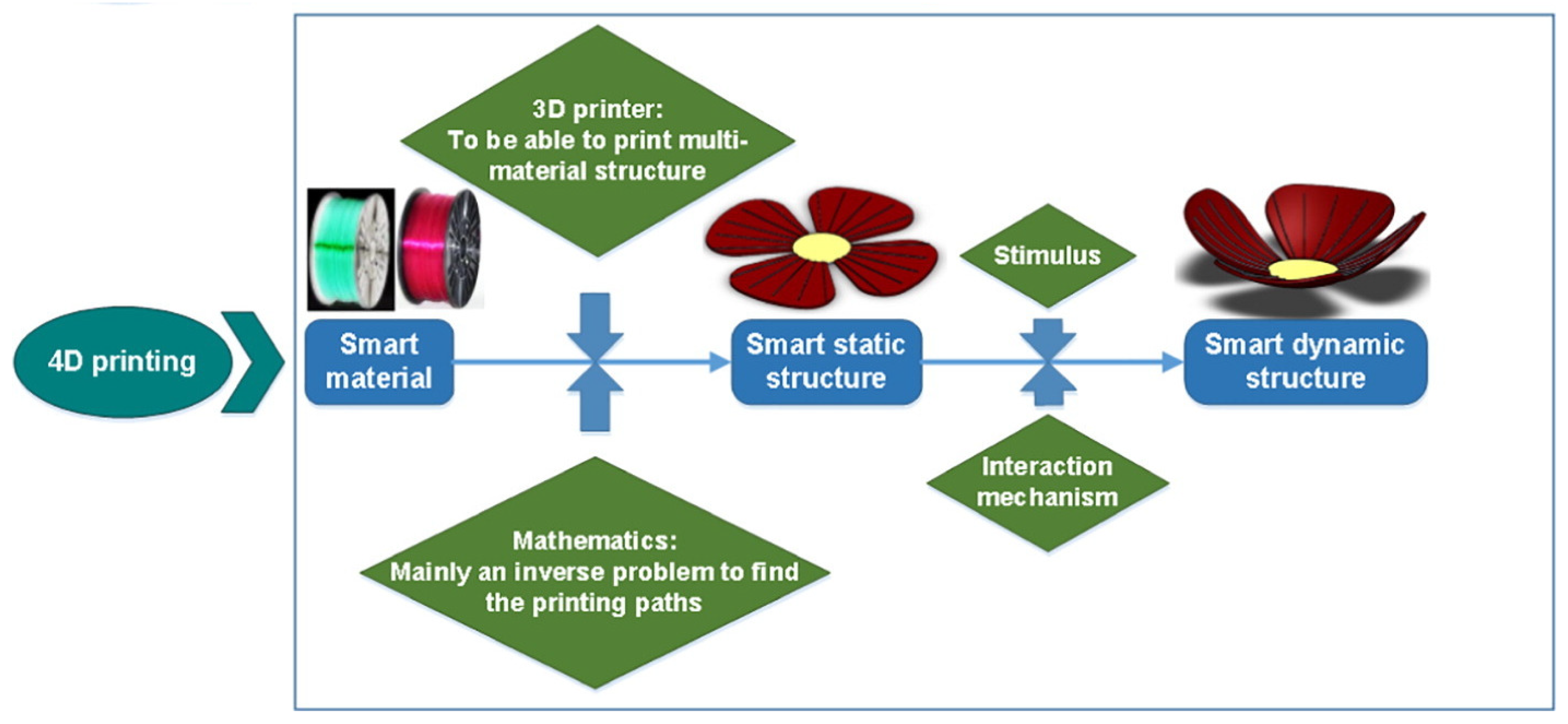
Figure 1. The 4D printing-fabrication process for dynamic structures, highlighting the role of each 4D printing feature. Reprinted with permission from Ref. [9]. Copyright 2017 Elsevier.
Jmmp 08 00164 g001
Figure 2. Distribution of articles searched with the keywords “4D printing” and “electronics” analysing Scopus and Web of Science results.
Jmmp 08 00164 g002
Figure 3. Fabrication steps of O-EGaIn electronic components on the surface of different shapes. Reprinted with permission from Ref. [14]. Copyright 2021 Elsevier.
Jmmp 08 00164 g003
Figure 4. Fractal Hilbert dipole antenna printed with FFF 3D printer using PU-based ECA.
Jmmp 08 00164 g004
Figure 5. DR reflectarray antenna fabricated using FFF: (a) the whole simulated model, comprising the feed horns, to irradiate the antenna; (b) the actual fabricated prototype used for antenna testing; (c) top view of the FFF fabricated array of DR antennas. Reprinted from Ref. [20].
Jmmp 08 00164 g005
Figure 6. Self-folding conformable electronics FFF printed. Used with permission from Association for Computing Machinery, permission conveyed through Copyright Clearence Center, Inc. 2020 [22].
Jmmp 08 00164 g006
Figure 7. Electrical-responsive structure, fabricated using DIW: (a) theoretical explanation of shape-changing behaviour of the PLMC/CNT ink under electrical stimulation; (b) illustration of DIW fabrication of the U-shape sensors; (c) illustration of the shape-changing behaviour application for liquid sensing. Reprinted with permission from Ref. [24]. Copyright 2019 Elsevier.
Jmmp 08 00164 g007
Figure 8. Working principle of EHD, with the component scheme. Reprinted from [26].
Jmmp 08 00164 g008
Figure 9. Hybrid AM-fabrication technology example for digital LED light fabrication: (a) schematic representation of the fabricated device; (b) fabricated device; (c) fabricated device turned on through the external power supply, directly connected to the LED chip with silver traces. Reprinted with permission from Ref. [27]. Copyright 2019 Elsevier.
Jmmp 08 00164 g009
Figure 10. The smart cap for packaged food monitoring: (a) the CAD models of the cap components, fabricated through FFF (top/bottom contacts) and PolyJet (cap, spring, seeger, and bolt); (b) the printed cap assembled and mounted on the plastic bottle for open/close tests. Used with permission conveyed through Copyright Clearance Center, Inc. 2018 [32].
Jmmp 08 00164 g010
Figure 11. Shape memory combination with the piezoelectric effect. (a) Shape memory loading cycle and (b) correlated piezoelectric effect. (c) Voltage output from the structure deforming under 2 g weight at 100 °C. Reprinted with permission from Ref. [64]. Copyright 2020 Elsevier.
Jmmp 08 00164 g011
Figure 12. Three different applications of the LCE–LM structure to show its versatility:(i) a twisting actuator with SDM resistors and an LED able to operate with a 90 °C twist. (ii) Capacitive touch sensor. (iii) An LCE crawler with an on/off photoresistor. Using 3D-printed feet, the crawler can store energy as it is heated and then pull itself in the red arrow direction as it cools. Adapted from [67].
Jmmp 08 00164 g012
Figure 13. Laser–engraved ceramic precursor MEMS structure. Reprinted from [86].
Jmmp 08 00164 g013
Table 1. A list of factors that should be considered during 4D printing design.
Factors Responsible for 4D Printing
AM processesFused filament fabrication, stereolithography, digital light projection, inkjet, selective laser sintering
Smart materialsShape memory polymers (SMP), stimuli-responsive
StimuliPhysical, chemical, biological
Interaction mechanismsMechanical, physical manipulation
Mathematical modelsForward and backward production
Table 2. A summary of the previously mentioned examples of 4D-printing applications in electronics.
ApplicationFabrication TechnologyAM CategoryExamplesRef.
ActuatorsVat photopolymerizationDLPO-EGaIn thermoresponsive electronics (functional electronics)[14]
Multi-technology platformIJP/DIW/FFF/AJ/PnPSoft pneumatic actuator (soft robotic)
Digital LED lamp
LCE-based actuator (soft robotics)
[27,31]
AntennasFFFFFF3D Hilbert dipole antenna
Hemispherical DRA with a metallic cap
Millimeter-wave dual-polarized DR reflectarray
[18,19,20]
Self-morphing circuitFFFFFFThermally activated self-folding electronics (origami structure)[22]
SensorsExtrusion-basedDIWShape-changing, electrical responsive liquid sensor
Resistive strain and flexible sensors
[24,25]
DIW/EHDTemperature and humidity sensor[25]
Disclaimer/Publisher’s Note: The statements, opinions and data contained in all publications are solely those of the individual author(s) and contributor(s) and not of MDPI and/or the editor(s). MDPI and/or the editor(s) disclaim responsibility for any injury to people or property resulting from any ideas, methods, instructions or products referred to in the content.