
Electrochemical Growth and Structural Study of the AlxGa1−xAs Nanowhisker Layer on the GaAs Surface

 ,
,  ,
, 
Abstract
:1. Introduction
2. Materials and Methods
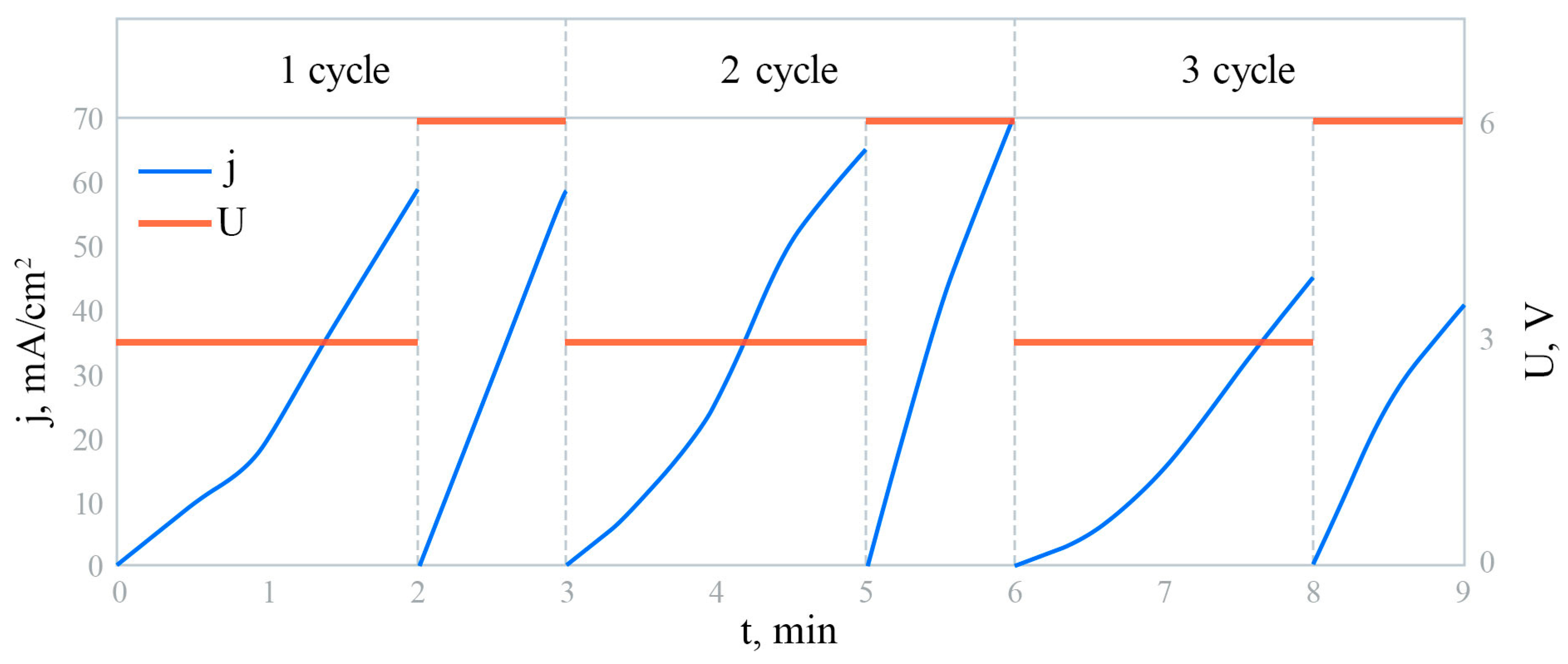
2.1. Experimental Method
2.2. Research Methods
3. Results
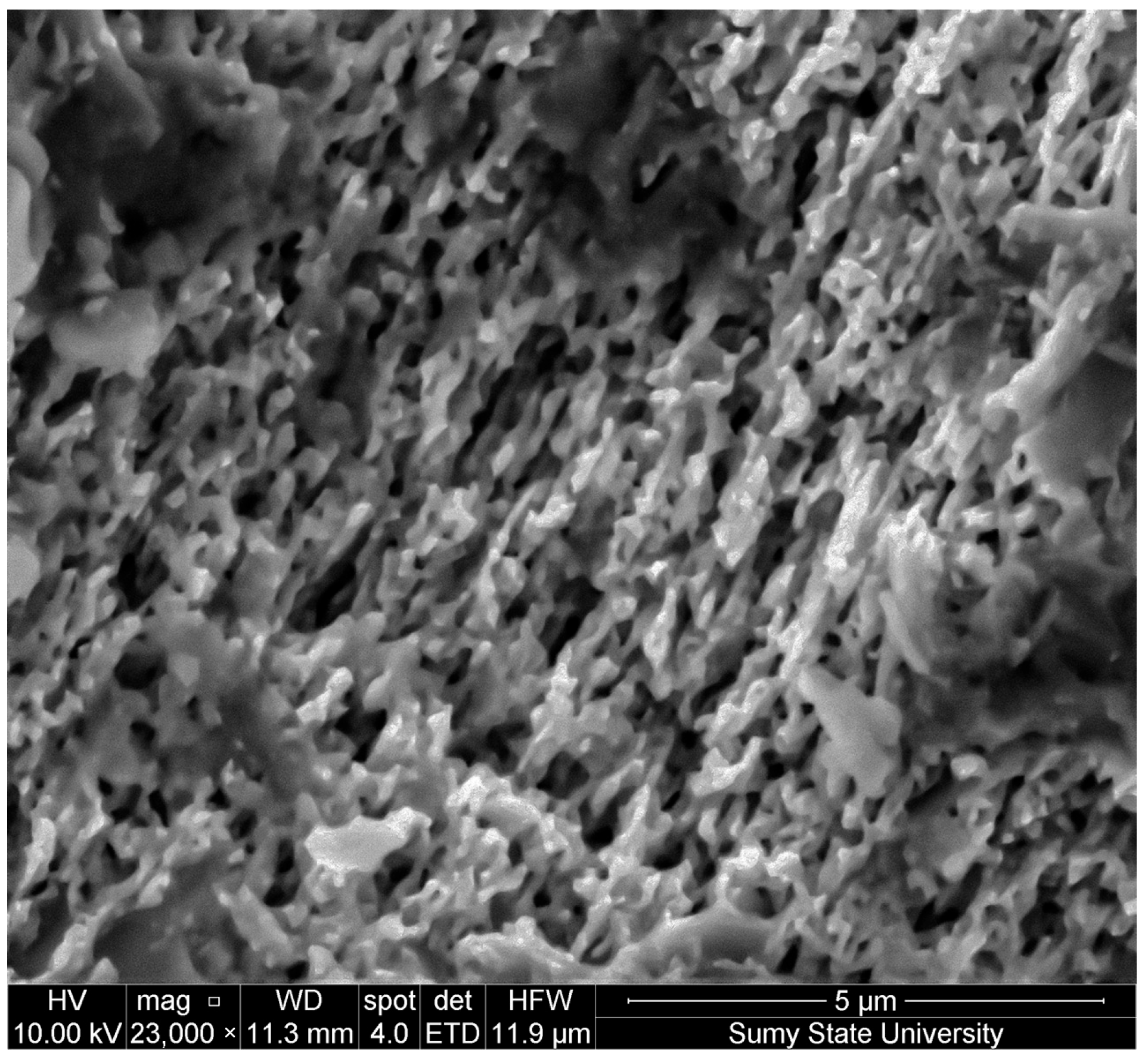
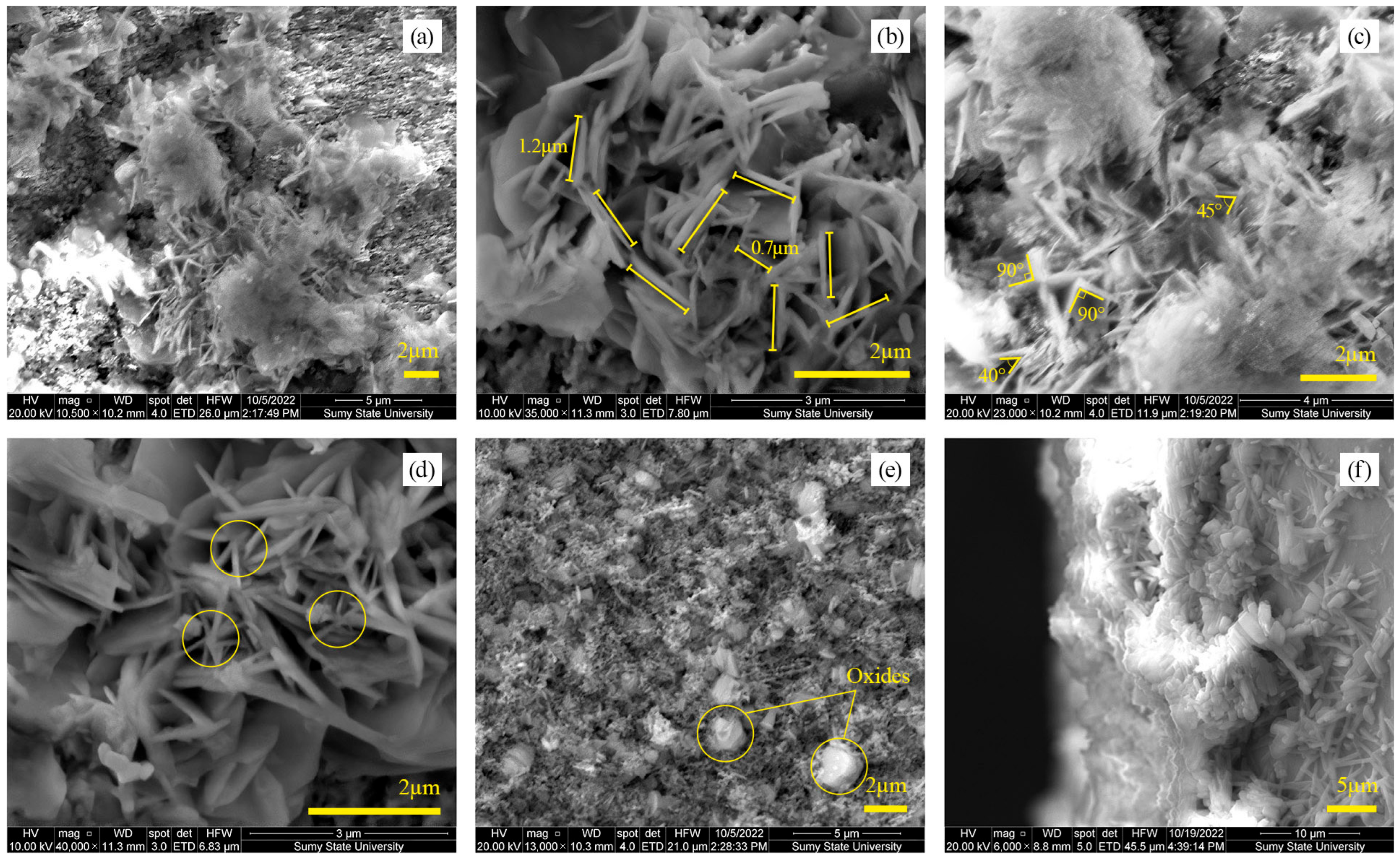
3.1. SEM Analysis
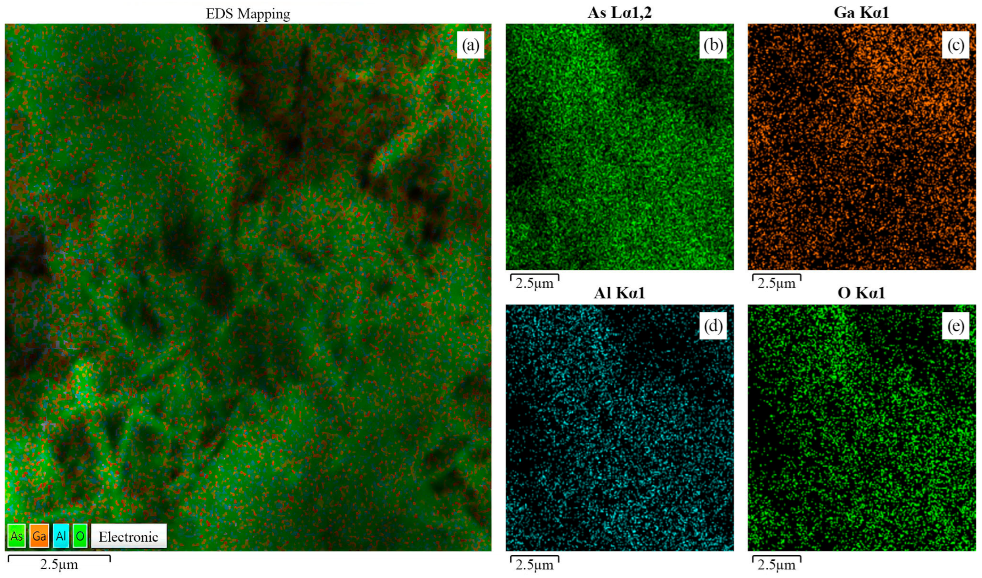
3.2. EDX Analysis
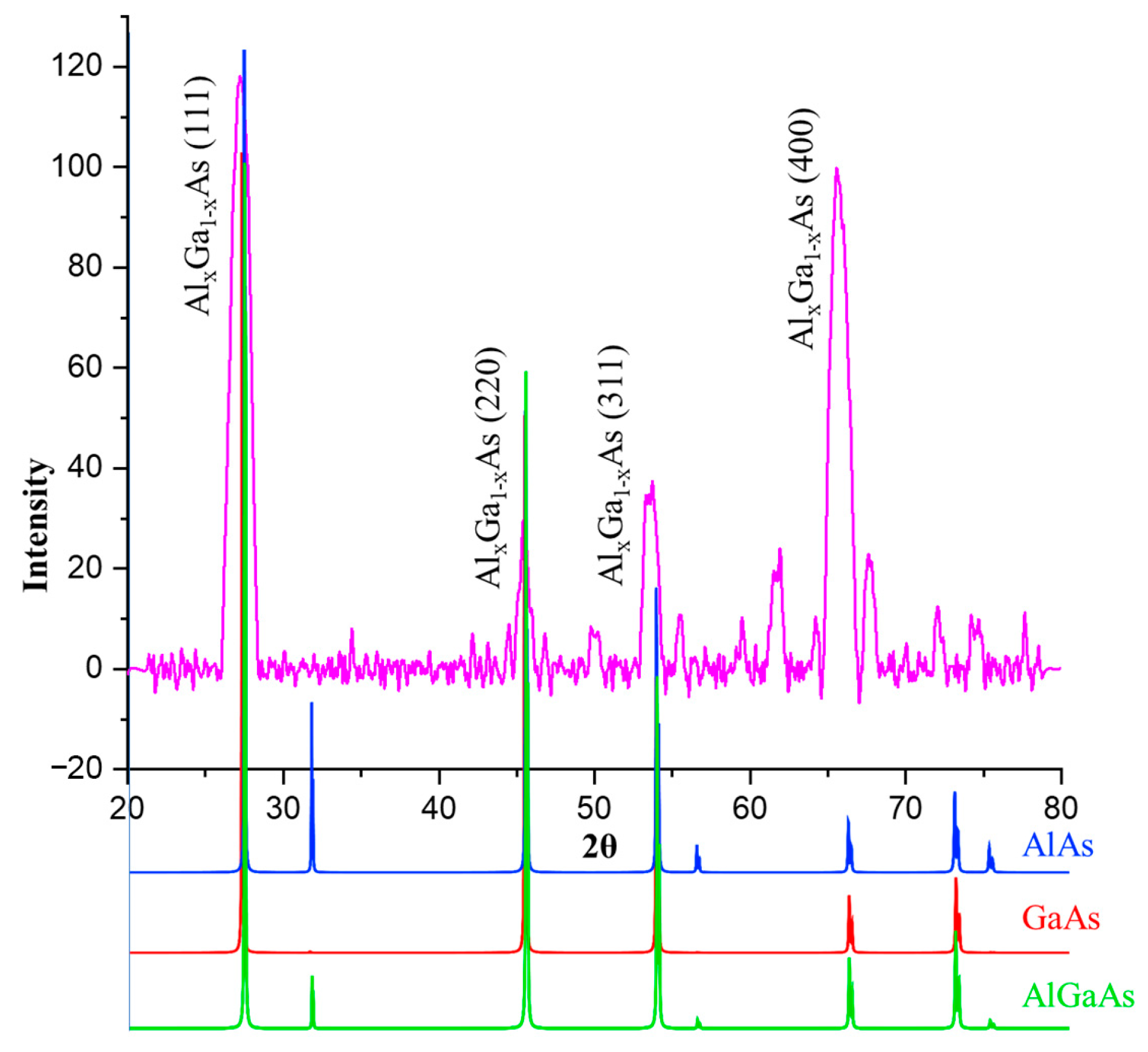
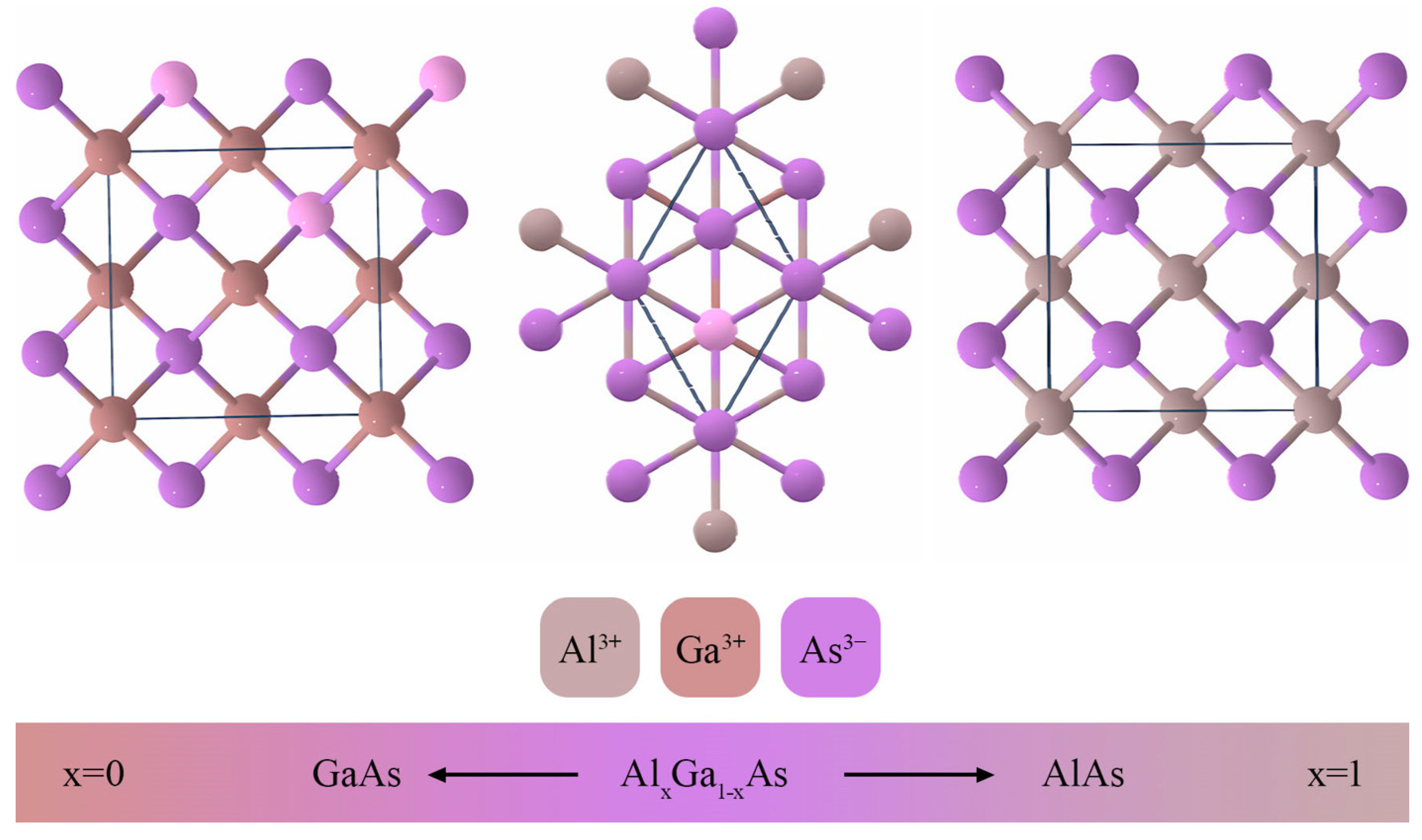
3.3. XRD Analysis
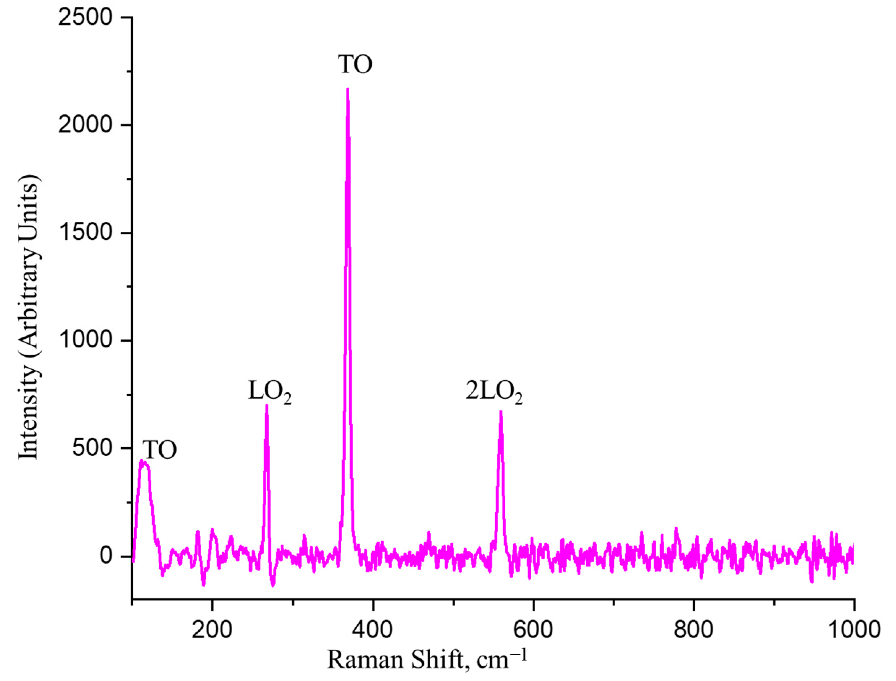
3.4. Raman Analysis
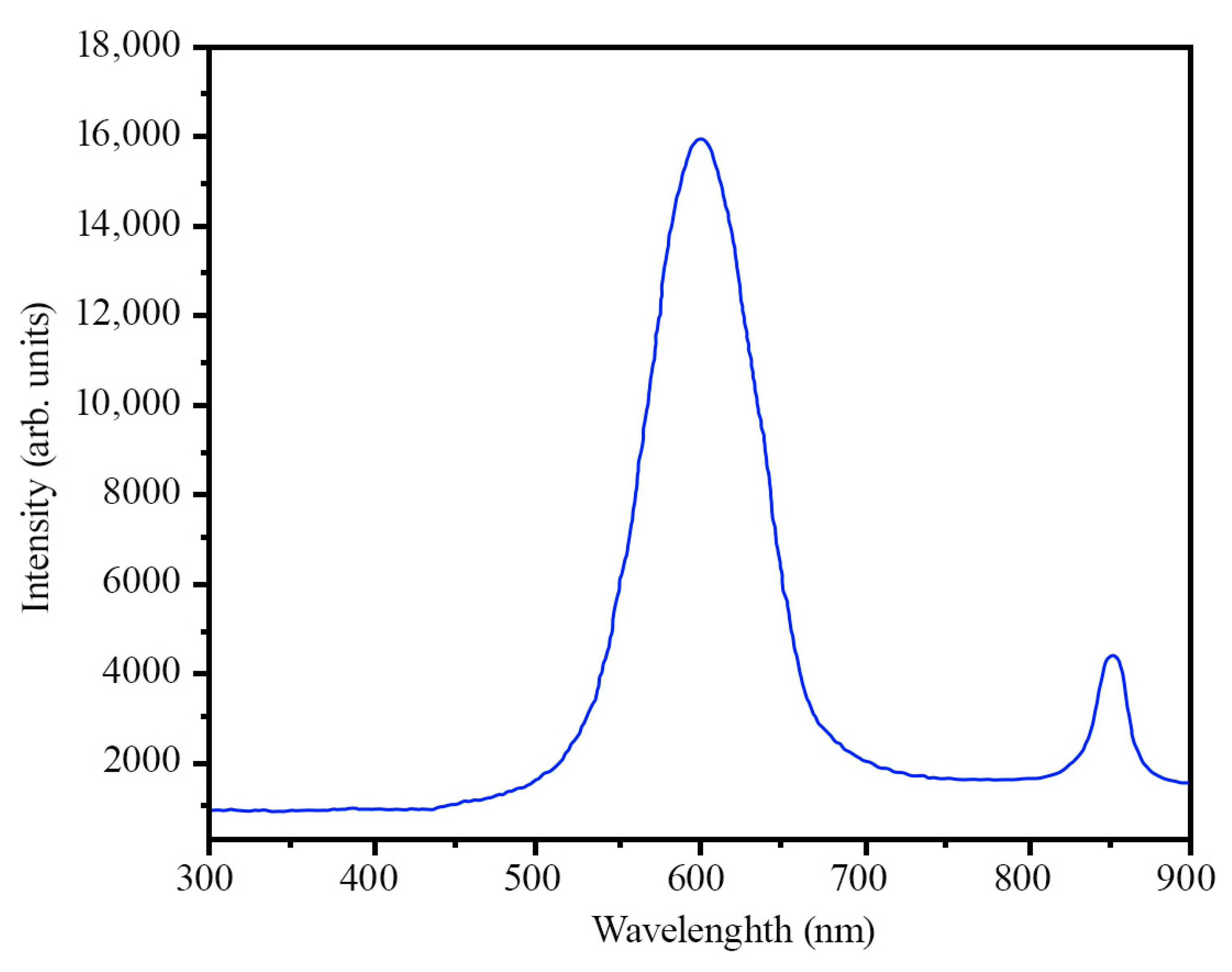
3.5. PL Analysis
4. Discussion
- The Frank–van der Merwe growth mechanism is characterized by layer-by-layer film growth and is typical for cases where the crystalline lattices of the substrate and film are well matched [63];
- The Volmer–Weber mechanism, on the contrary, is characterized by island growth and occurs mainly in cases where the crystalline lattices have pretty different parameters [64];
- The Stranski–Krastanov mechanism is characterized by layer-plus-island growth and is a “compromise mechanism” [65].
5. Conclusions
Author Contributions
Funding
Data Availability Statement
Conflicts of Interest
References
- Su, Z.; Yang, Y.; Huang, Q.; Chen, R.; Ge, W.; Fang, Z.; Huang, F.; Wang, X. Designed biomass materials for “green” electronics: A review of materials, fabrications, devices, and perspectives. Prog. Mater. Sci. 2022, 125, 100917. [Google Scholar] [CrossRef]
- Mahmood, K.; Sarwar, S.; Mehran, M.T. Current status of electron transport layers in perovskite solar cells: Materials and properties. RSC Adv. 2017, 7, 17044–17062. [Google Scholar] [CrossRef]
- Suchikova, Y.A.; Kidalov, V.V.; Sukach, G.A. Influence of the carrier concentration of indium phosphide on the porous layer formation. J. Nano Electron. Phys. 2010, 2, 75–81. [Google Scholar]
- Vadakkedath Gopi, S.; Spalatu, N.; Basnayaka, M.; Krautmann, R.; Katerski, A.; Josepson, R.; Grzibovskis, R.; Vembris, A.; Oja Acik, I. Post deposition annealing effect on properties of CdS films and its impact on CdS/Sb2Se3 solar cells performance. Front. Energy Res. 2023, 11, 1162576. [Google Scholar] [CrossRef]
- Liudziute, M.; Zalenkiene, S.; Ivanauskas, R.; Ancutiene, I. Impact of Polyamide Surface Preparation on the Formation of Mixed CdS-CdTe Layers. Crystals 2023, 13, 730. [Google Scholar] [CrossRef]
- Balakhayeva, R.; Akilbekov, A.; Baimukhanov, Z.; Usseinov, A.; Giniyatova, S.; Zdorovets, M.; Vlasukova, L.; Popov, A.I.; Dauletbekova, A. CdTe Nanocrystal Synthesis in SiO2/Si Ion-Track Template: The Study of Electronic and Structural Properties. Phys. Status Solidi 2021, 218, 2000231. [Google Scholar] [CrossRef]
- Heredia-Cancino, J.A.; Mendoza-Peña, K.J.; Higuera-Valenzuela, H.J.; Soto, B.M.A.; Ochoa-Landín, R.; Castillo, S.J. Synthesis Optimization of Cadmium Carbonate Films as Potential Precursor to Produce CdSe, CdTe, and CdO Films. Coatings 2022, 12, 1691. [Google Scholar] [CrossRef]
- Kalyk, F.; Žalga, A.; Vasiliauskas, A.; Tamulevičius, T.; Tamulevičius, S.; Abakevičienė, B. Synthesis and Electron-Beam Evaporation of Gadolinium-Doped Ceria Thin Films. Coatings 2022, 12, 747. [Google Scholar] [CrossRef]
- Tamulevičius, S.; Valkonen, M.P.; Laukaitis, G.; Lindroos, S.; Leskelä, M. Stress and surface studies of SILAR grown CdS thin films on GaAs (100). Thin Solid Film. 1999, 355, 430–434. [Google Scholar] [CrossRef]
- Ščajev, P.; Miasojedovas, S.; Mekys, A.; Onufrijevs, P.; Cheng, H.-H. Time-Resolved Photoluminescence in GeSn Film by New Infrared Streak Camera Attachment Based on a Broadband Light Upconversion. Coatings 2023, 13, 111. [Google Scholar] [CrossRef]
- Levinas, R.; Tsyntsaru, N.; Cesiulis, H.; Viter, R.; Grundsteins, K.; Tamašauskaitė-Tamašiūnaitė, L.; Norkus, E. Electrochemical Synthesis of a WO3/MoSx Heterostructured Bifunctional Catalyst for Efficient Overall Water Splitting. Coatings 2023, 13, 673. [Google Scholar] [CrossRef]
- Vihodceva, S.; Šutka, A.; Otsus, M.; Vija, H.; Grase, L.; Kahru, A.; Kasemets, K. Visible-Light Active Flexible and Durable Photocatalytic Antibacterial Ethylene-co-vinyl Acetate—Ag/AgCl/α-Fe2O3 Composite Coating. Nanomaterials 2022, 12, 1984. [Google Scholar] [CrossRef] [PubMed]
- Balakhayeva, R.; Akilbekov, A.; Baimukhanov, Z.; Giniyatova, S.; Zdorovets, M.; Gorin, Y.; Popov, A.I.; Dauletbekova, A. Structure properties of CdTe nanocrystals created in SiO2/Si ion track Templates. Surf. Coat. Technol. 2020, 401, 126269. [Google Scholar] [CrossRef]
- Karipbayev, Z.T.; Kumarbekov, K.; Manika, I.; Suchikova, Y.; Popov, A.I. Optical, Structural, and Mechanical Properties of Gd3Ga5O12 Single Crystals Irradiated with 84Kr+ Ions. Phys. Status Solidi B 2022, 259, 2100415. [Google Scholar] [CrossRef]
- Yana, S. Porous indium phosphide: Preparation and properties. In Handbook of Nanoelectrochemistry: Electrochemical Synthesis Methods, Properties, and Characterization Techniques, 1st ed.; Springer: Cham, Switzerland, 2016; pp. 283–306. [Google Scholar] [CrossRef]
- Suchikova, Y.; Kovachov, S.; Bohdanov, I.; Moskina, A.; Popov, A. Characterization of CdxTeyOz/CdS/ZnO Heterostructures Synthesized by the SILAR Method. Coatings 2023, 13, 639. [Google Scholar] [CrossRef]
- Suchikova, Y.; Kovachov, S.; Bohdanov, I.; Karipbaev, Z.T.; Pankratov, V.; Popov, A.I. Study of the structural and morphological characteristics of the CdxTeyOz nanocomposite obtained on the surface of the CdS/ZnO heterostructure by the SILAR method. Appl. Phys. A 2023, 129, 499. [Google Scholar] [CrossRef]
- Grechenkov, J.; Gopejenko, A.; Bocharov, D.; Isakoviča, I.; Popov, A.I.; Brik, M.G.; Piskunov, S. Ab Initio Modeling of CuGa1−xInxS2, CuGaS2(1−x)Se2x and Ag1−xCuxGaS2 Chalcopyrite Solid Solutions for Photovoltaic Applications. Energies 2023, 16, 4823. [Google Scholar] [CrossRef]
- Kılıç, H.S.; Gezgin, S.Y.; Üzüm, Ö.; Gündoğdu, Y. Third order nonlinear optical properties of copper indium gallium selenide (CIGS) nanocrystal thin films. Appl. Phys. B 2022, 128, 105. [Google Scholar] [CrossRef]
- Sychikova, Y.A.; Kidalov, V.V.; Sukach, G.A. Dependence of the threshold voltage in indium-phosphide pore formation on the electrolyte composition. J. Surface Investig. 2013, 7, 626–630. [Google Scholar] [CrossRef]
- Suohikova, Y.; Vambol, S.; Vambol, V.; Mozaffari, N. Justification of the most rational method for the nanostructures synthesis on the semiconductors surface. J. Achiev. Mater. Manuf. Eng. 2019, 92, 19–28. [Google Scholar] [CrossRef]
- Vambol, S.O.; Bogdanov, I.T.; Vambol, V.V.; Suchikova, Y.O.; Kovachov, S.S. Correlation between technological factors of synthesis of por-GaP and its acquired properties. Nanosist. Nanomater. Nanotehnol. 2018, 16, 657–670. [Google Scholar]
- Foell, H.; Langa, S.; Carstensen, J.; Christophersen, M.; Tiginyanu, I.M. Pores in III–V semiconductors. Adv. Mater. 2003, 15, 183–198. [Google Scholar] [CrossRef]
- Langa, S.; Carstensen, J.; Christophersen, M.; Steen, K.; Frey, S.; Tiginyanu, I.M.; Föll, H. Uniform and nonuniform nucleation of pores during the anodization of Si, Ge, and III-V semiconductors. J. Electrochem. Soc. 2005, 152, C525. [Google Scholar] [CrossRef]
- Zhang, L.; Zheng, Z.; Lou, X. A review of WBG and Si devices hybrid applications. Chin. J. Electr. Eng. 2021, 7, 1–20. [Google Scholar] [CrossRef]
- Sobolev, M.S.; Ilkiv, I.V.; Lazarenko, A.A.; Mizerov, A.M.; Nikitina, E.V.; Pirogov, E.V.; Bouravleuv, A.D. Monolith GaAsP/Si dual-junction solar cells grown by MBE. J. Phys. Conf. Ser. 2019, 1410, 012040. [Google Scholar] [CrossRef]
- Zhang, W.W.; Qi, H.; Ji, Y.K.; He, M.J.; Ren, Y.T.; Li, Y. Boosting photoelectric performance of thin film GaAs solar cell based on multi-objective optimization for solar energy utilization. Solar Energy 2021, 230, 1122–1132. [Google Scholar] [CrossRef]
- Ajayan, J.; Nirmal, D.; Mohankumar, P.; Kuriyan, D.; Fletcher, A.A.; Arivazhagan, L.; Kumar, B.S. GaAs metamorphic high electron mobility transistors for future deep space-biomedical-millitary and communication system applications: A review. Microelectron. J. 2019, 92, 104604. [Google Scholar] [CrossRef]
- Steiner, M.A.; France, R.M.; Buencuerpo, J.; Geisz, J.F.; Nielsen, M.P.; Pusch, A.; Olavarria, W.J.; Young, M.; Ekins-Daukes, N.J. High efficiency inverted GaAs and GaInP/GaAs solar cells with strain-balanced GaInAs/GaAsP quantum wells. Adv. Energy Mater. 2020, 11, 2002874. [Google Scholar] [CrossRef]
- Quandt, D.; Arsenijević, D.; Strittmatter, A.; Bimberg, D.H. Static and Dynamic Characteristics of In (AsSb)/GaAs Submonolayer Lasers. EEE J. Quantum Electron. 2019, 55, 1–7. [Google Scholar] [CrossRef]
- Zhang, J.; Itzler, M.A.; Zbinden, H.; Pan, J.W. Advances in InGaAs/InP single-photon detector systems for quantum communication. Light. Sci. Appl. 2015, 4, e286. [Google Scholar] [CrossRef]
- Lindsey, Z.R.; West, M.; Jacobson, P.; Ray, J.R. Benchtop Electrochemical Growth and Controlled Alloying of Polycrystalline In x Ga1–x As Thin Films. Cryst. Growth Des. 2022, 22, 4228–4235. [Google Scholar] [CrossRef]
- Zhang, X.; Yi, R.; Gagrani, N.; Li, Z.; Zhang, F.; Gan, X.; Yao, X.; Yuan, X.; Wang, N.; Zhao, J.; et al. Ultralow Threshold, Single-Mode InGaAs/GaAs Multiquantum Disk Nanowire Lasers. ACS Nano 2021, 15, 9126–9133. [Google Scholar] [CrossRef] [PubMed]
- Woods-Robinson, R.; Han, Y.; Zhang, H.; Ablekim, T.; Khan, I.; Persson, K.A.; Zakutayev, A. Wide band gap chalcogenide semiconductors. Chem. Rev. 2020, 120, 4007–4055. [Google Scholar] [CrossRef] [PubMed]
- Zhang, B.; Wang, S. A survey of EMI research in power electronics systems with wide-bandgap semiconductor devices. IEEE J. Emerg. Sel. Top. Power Electron. 2019, 8, 626–643. [Google Scholar] [CrossRef]
- Shur, M. Wide band gap semiconductor technology: State-of-the-art. Solid-State Electron. 2019, 155, 65–75. [Google Scholar] [CrossRef]
- Zheng, S.; Xiao, S.; Peng, K.; Pan, Y.; Yang, X.; Lu, X.; Han, G.; Zhang, B.; Zhou, Z.; Wang, G.; et al. Symmetry-Guaranteed High Carrier Mobility in Quasi-2D Thermoelectric Semiconductors. Adv. Mater. 2023, 35, 2210380. [Google Scholar] [CrossRef]
- Gil-Corrales, J.A.; Morales, A.L.; Yücel, M.B.; Kasapoglu, E.; Duque, C.A. Electronic Transport Properties in GaAs/AlGaAs and InSe/InP Finite Superlattices under the Effect of a Non-Resonant Intense Laser Field and Considering Geometric Modifications. Int. J. Mol. Sci. 2022, 23, 5169. [Google Scholar] [CrossRef] [PubMed]
- Kawaharazuka, A.; Onomitsu, K.; Nishinaga, J.; Horikoshi, Y. Effect of excitons on the absorption in the solar-cell with AlGaAs/GaAs superlattice grown by molecular beam epitaxy. J. Cryst. Growth 2011, 323, 504–507. [Google Scholar] [CrossRef]
- Bahar, M.K.; Rodríguez-Magdaleno, K.A.; Martínez-Orozco, J.C.; Mora-Ramos, M.E.; Ungan, F.A.T. Optical properties of a triple AlGaAs/GaAs quantum well purported for quantum cascade laser active region. Mater. Today Commun. 2020, 26, 101936. [Google Scholar] [CrossRef]
- Suchikova, Y.O.; Kovachov, S.S.; Lazarenko, A.S.; Bardus, I.O.; Tikhovod, K.; Hurenko, O.I.; Bohdanov, I.T. Oxidation of the n-GaAs Surface: Morphological and Kinetic Analysis. J. Nano-Electron. Phys. 2022, 14, 03033. [Google Scholar] [CrossRef]
- Suchikova, Y.; Lazarenko, A.; Kovachov, S.; Usseinov, A.; Karipbaev, Z.; Popov, A.I. Formation of porous Ga2O3/GaAs layers for electronic devices. In Proceedings of the 16th International Conference on Advanced Trends in Radioelectronics, Telecommunications and Computer Engineering, TCSET, Lviv-Slavske, Ukraine, 22–26 February 2022; pp. 410–413. [Google Scholar] [CrossRef]
- Kovachov, S.; Bohdanov, I.; Karipbayev, Z.; Suchikova, Y.; Tsebriienko, T.; Popov, A.I. Layer-by-Layer Synthesis and Analysis of the Phase Composition of CdxTeyOz/CdS/por-ZnO/ZnO Heterostructure. In Proceedings of the 2022 IEEE 3rd KhPI Week on Advanced Technology, KhPI Week, Kharkiv, Ukraine, 3–7 October 2022. [Google Scholar] [CrossRef]
- Kovachov, S.; Bohdanov, I.; Bardus, I.; Drozhcha, D.; Tikhovod, K.; Khrekin, A.; Bondarenko, V.; Kosogov, I.; Suchikova, Y. About synthesis mechanism of periodic oxide nanocrystallites on surface of single-crystal. Phys. Chem. Solid State 2023, 24, 159–165. [Google Scholar] [CrossRef]
- Suchikova, Y.; Bogdanov, I.; Kovachov, S.; Kamensky, D.; Myroshnychenko, V.; Panova, N. Optimal ranges determination of morphological parameters of nanopatterned semiconductors quality for solar cells. Arch. Mater. Sci. Eng. 2020, 1, 15–24. [Google Scholar] [CrossRef]
- Ko, F.K.; Kuznetsov, V.; Flahaut, E.; Peigney, A.; Laurent, C.; Prinz, V.Y.; Mani, R.C.; Sunkara, M.K.; Baldwin, R.P.; Capelli, E.; et al. Formation of Nanofibers and Nanotubes Production. In Nanoengineered Nanofibrous Materials; Guceri, S., Gogotsi, Y.G., Kuznetsov, V., Eds.; NATO Science Series 169; Springer: Dordrecht, The Netherlands, 2004. [Google Scholar] [CrossRef]
- Shetti, N.P.; Malode, S.J.; Nayak, D.S.; Bagihalli, G.B.; Kalanur, S.S.; Malladi, R.S.; Reddy, C.V.; Aminabhavi, T.M.; Reddy, K.R. Fabrication of ZnO nanoparticles modified sensor for electrochemical oxidation of methdilazine. Appl. Surf. Sci. 2019, 496, 143656. [Google Scholar] [CrossRef]
- Bisquert, J.; Fabregat-Santiago, F.; Mora-Seró, I.; Garcia-Belmonte, G.; Barea, E.M.; Palomares, E. A review of recent results on electrochemical determination of the density of electronic states of nanostructured metal-oxide semiconductors and organic hole conductors. Inorg. Chim. Acta 2008, 361, 684–698. [Google Scholar] [CrossRef]
- Islam, S.; Mia, M.; Shah, S.S.; Naher, S.; Shaikh, M.N.; Aziz, A.; Ahammad, A.J.S. Recent Advancements in Electrochemical Deposition of Metal-Based Electrode Materials for Electrochemical Supercapacitors. Chem. Rec. 2022, 22, e202200013. [Google Scholar] [CrossRef] [PubMed]
- Liu, X.; Wang, F.; Wang, Q. Nanostructure-based WO3 photoanodes for photoelectrochemical water splitting. Phys. Chem. Chem. Phys. 2012, 14, 7894–7911. [Google Scholar] [CrossRef]
- Suchikova, Y.; Kovachov, S.; Bohdanov, I. Formation of oxide crystallites on the porous GaAs surface by electrochemical deposition. Nanomater. Nanotechnol. 2022, 12, 1–12. [Google Scholar] [CrossRef]
- Vambol, S.O.; Bohdanov, I.T.; Vambol, V.V.; Nestorenko, T.P.; Onyschenko, S.V. Formation of filamentary structures of oxide on the surface of monocrystalline gallium arsenide. J. Nano-Electron. Phys. 2017, 9, 06016. [Google Scholar] [CrossRef]
- Scherrer, P. Determination of the size and internal structure of colloidal particles using X-rays. Nachr. Ges. Wiss. Göttingen 1918, 2, 98–100. [Google Scholar]
- Langford, J.; Wilson, A. Scherrer after sixty years: A survey and some new results in the determination of crystallite size. J. Appl. Crystallogr. 1978, 11, 102–113. [Google Scholar] [CrossRef]
- Kuryliuk, V.; Podolian, A.; Korotchenkov, O. Acoustically driven charge separation in semiconductor heterostructures sensed by optical spectroscopy techniques. Open Phys. 2010, 8, 1. [Google Scholar] [CrossRef]
- Kim, O.K.; Spitzer, W.G. Infrared reflectivity spectra and Raman spectra of Ga1−xAlxAs mixed crystals. J. Appl. Phys. 1979, 50, 4362–4370. [Google Scholar] [CrossRef]
- Nakahara, J.; Ichimori, T.; Minomura, S.; Kukimoto, H. Raman Spectra in AlxGa1-xAs under High Pressure. J. Phys. Soc. Jpn. 1987, 56, 1010–1016. [Google Scholar] [CrossRef]
- Guo, L.W.; Han, Y.J.; Hu, C.Y.; Tan, P.H.; Yang, F.H.; Huang, Q.; Zhou, J.M. Raman study of low-temperature-grown Al0.29Ga0.71As/GaAs photorefractive materials. Phys. Rev. B 2002, 65, 125325. [Google Scholar] [CrossRef]
- Wang, Y.; Zahid, F.; Zhu, Y.; Wang, J.; Guo, H. Band offset of GaAs/AlxGa1−xAs heterojunctions from atomistic first principles. Appl. Phys. Lett. 2013, 102, 132109. [Google Scholar] [CrossRef]
- Adachi, S. GaAs and Related Materials; World Scientific: Singapore, 1994. [Google Scholar] [CrossRef]
- Brown, M.A.; Abbas, Z.; Kleibert, A.; May, S.; Squires, T.M. Determination of surface potential and electrical double-layer structure at the aqueous electrolyte-nanoparticle interface. Phys. Rev. X 2016, 6, 011007. [Google Scholar] [CrossRef]
- Suchikova, Y.; Kovachov, S.; Lazarenko, A.; Bohdanov, I. Research of synthesis conditions and structural features of heterostructure AlXGa1−XAs/GaAs of the ‘desert rose’ type. Appl. Surf. Sci. Adv. 2022, 12, 100327. [Google Scholar] [CrossRef]
- Sun, X.W.; Huang, H.C.; Kwok, H.S. On the initial growth of indium tin oxide on glass. Appl. Phys. Lett. 1996, 68, 2663–2665. [Google Scholar] [CrossRef]
- Floro, J.A.; Hearne, S.J.; Hunter, J.A.; Seel, S.C.; Thompson, C.V. The dynamic competition between stress generation and relaxation mechanisms during coalescence of Volmer-Weber thin films. J. Appl. Phys. 2001, 89, 4886–4897. [Google Scholar] [CrossRef]
- Pan, L.; Lew, K.-K.; Redwing, J.M.; Dickey, E.C. Stranski-Krastanow growth of germanium on silicon nanowires. Nano Lett. 2005, 5, 1081–1085. [Google Scholar] [CrossRef]


| Elements | At, % | |||
|---|---|---|---|---|
| 1 | 2 | 3 | 4 | |
| O | 7.35 | 6.23 | 7.01 | 6.91 |
| As | 41.54 | 42.12 | 40.69 | 42.05 |
| Ga | 26.74 | 26.95 | 26.51 | 27.14 |
| Al | 24.37 | 24.7 | 25.79 | 23.90 |
| Total | 100 | 100 | 100 | 100 |
| Elements | Relative Units, % | |||
|---|---|---|---|---|
| 1 | 2 | 3 | 4 | |
| Ga/As | 0.64 | 0.64 | 0.65 | 0.65 |
| Al/As | 0.59 | 0.59 | 0.63 | 0.57 |
| Al/Ga | 0.911 | 0.916 | 0.973 | 0.881 |
| (Al + Ga)/As | 1.23 | 1.23 | 1.28 | 1.22 |
| Parameters | AlAs | Al0.71Ga0.29As | GaAs |
|---|---|---|---|
| Crystal system | Cubic | Cubic | Cubic |
| Space group | F-43m | F-43m | F-43m |
| Space group number | 216 | 216 | 216 |
| a = b = c (A) | 5.6620 | 5.6604 | 5.5080 |
| α = β = γ (o) | 90.00 | 90.00 | 90.00 |
| Calculated density (g/cm3) | 3.73 | 4.19 | 5.75 |
| Volume of cell (106 pm3) | 181.51 | 181.36 | 167.10 |
| Parameters | Identification | ||
|---|---|---|---|
| Raman Shift | Phonon Mode | Assignment | |
| 1 | 110 | TO | Ga-As, Al-As |
| 2 | 267 | LO2 | Ga-As |
| 3 | 369 | TO | Al-As |
| 4 | 559 | 2LO2 | Ga-As |
Disclaimer/Publisher’s Note: The statements, opinions and data contained in all publications are solely those of the individual author(s) and contributor(s) and not of MDPI and/or the editor(s). MDPI and/or the editor(s) disclaim responsibility for any injury to people or property resulting from any ideas, methods, instructions or products referred to in the content. |
© 2023 by the authors. Licensee MDPI, Basel, Switzerland. This article is an open access article distributed under the terms and conditions of the Creative Commons Attribution (CC BY) license (https://creativecommons.org/licenses/by/4.0/).
Share and Cite
Suchikova, Y.; Kovachov, S.; Bohdanov, I.; Abdikadirova, A.A.; Kenzhina, I.; Popov, A.I. Electrochemical Growth and Structural Study of the AlxGa1−xAs Nanowhisker Layer on the GaAs Surface. J. Manuf. Mater. Process. 2023, 7, 153. https://doi.org/10.3390/jmmp7050153
Suchikova Y, Kovachov S, Bohdanov I, Abdikadirova AA, Kenzhina I, Popov AI. Electrochemical Growth and Structural Study of the AlxGa1−xAs Nanowhisker Layer on the GaAs Surface. Journal of Manufacturing and Materials Processing. 2023; 7(5):153. https://doi.org/10.3390/jmmp7050153
Chicago/Turabian StyleSuchikova, Yana, Sergii Kovachov, Ihor Bohdanov, Anar A. Abdikadirova, Inesh Kenzhina, and Anatoli I. Popov. 2023. "Electrochemical Growth and Structural Study of the AlxGa1−xAs Nanowhisker Layer on the GaAs Surface" Journal of Manufacturing and Materials Processing 7, no. 5: 153. https://doi.org/10.3390/jmmp7050153
APA StyleSuchikova, Y., Kovachov, S., Bohdanov, I., Abdikadirova, A. A., Kenzhina, I., & Popov, A. I. (2023). Electrochemical Growth and Structural Study of the AlxGa1−xAs Nanowhisker Layer on the GaAs Surface. Journal of Manufacturing and Materials Processing, 7(5), 153. https://doi.org/10.3390/jmmp7050153