
Article

Crack Intensity Reduction in Fe–6.5Si Alloy by Adding Cr and Controlling the Thermal Gradient

by
Masoud Ahmadnia
1,*,
Eskandar Fereiduni
1,2 and
Mohamed Elbestawi
1
1
Department of Mechanical Engineering, McMaster University, Hamilton, ON L8S 4L7, Canada
2
Acuren, Oakville, ON L6L 2X8, Canada
*
Author to whom correspondence should be addressed.
J. Manuf. Mater. Process. 2026, 10(9), 347; https://doi.org/10.3390/jmmp10090347
Submission received: 21 July 2026 / Revised: 26 August 2026 / Accepted: 31 August 2026 / Published: 8 September 2026

Abstract

The Fe–6.5 wt.% Si alloy is a promising soft magnetic material for electric motor applications owing to its high electrical resistivity and low core loss. However, the intrinsic brittleness of this alloy precludes fabrication of thin laminates using conventional rolling processes. Laser Powder Bed Fusion (LPBF) has therefore been considered as an alternative manufacturing route, offering both geometric flexibility and the inherent advantages of additive manufacturing. Nevertheless, successful LPBF processing of Fe–6.5 wt.% Si has remained challenging due to its high-silicon content. In this study, the Fe–6.5 wt.% Si alloy was modified by introducing 1 wt.% Cr, and LPBF process variables were optimized to yield defect-free parts. The effect of Cr addition on suppressing the disorder–order phase transformation during solidification was investigated through Thermo-Calc® thermodynamic simulations and quantified via X-ray diffraction phase analysis. Crack morphology analysis from optical micrographs revealed a marked reduction in both solidification and liquation cracks, attributed to the role of Cr in mitigating silicon segregation and consequently lowering the fraction of ordered phases. Preheating the build plate to 200 °C was found to effectively eliminate vertical cracks by reducing thermal stresses within the parts; however, a limited number of horizontal cracks initiated at the sample edges and propagated inward, likely due to elevated thermal gradients at the perimeter. To address this issue, sacrificial walls were introduced at distances of 1.0 mm and 0.2 mm from the cube edges, locally reducing the cooling rates and effectively increasing the primary dendrite arm spacing (PDAS). The reduced cooling rate also led to lower lattice misorientation, confirmed by electron backscatter diffraction (EBSD), and a significant decrease in the crack length from ~2 mm to ~0.7 mm.

1. Introduction

Soft magnetic materials are magnetic materials that can rapidly switch their magnetization direction based on the external magnetic field. Materials with a coercivity lower than 1000 A/m are usually considered soft magnetic materials and are extensively used in alternating current (AC) and direct current (DC) applications [1]. In AC magnetic applications, the direction and magnitude of the magnetic flux in the material is altered following the frequency of the external magnetic field. In addition to high permeability and good level of magnetic flux density as the key figures of merit in DC magnetic performance, minimizing the energy loss is the matter of greatest importance in AC applications.
One of the major parts of energy deficiency in soft magnetic materials is the iron loss, which quadratically increases with excitation frequency [2] and is accountable for about 20% energy loss of a 50 Hp electric motor [3]. In AC applications like electric motors, a higher working frequency improves the delivered power density of motors; thus, minimizing the iron loss of motors at high excitation frequencies is a key focus for much research conducted on soft magnetic materials.
According to the classical eddy-current theory [2], two main strategies could be implemented to reduce the iron loss: (1) decreasing the cross-section area of the material and (2) increasing the electrical resistivity of the soft magnetic material. In traditional methods of manufacturing, the thickness of material decreases to 0.35–0.6 mm [4] and a stack of these thin laminates with an insulator layer in between is fabricated as the cores of an electric motor. Although further reduction of laminates thickness to 0.1 mm to reduce iron loss is feasible and has been implemented to satisfy the requirements of aerospace applications [5], it is not popular due to the low stacking factor of the fabricated core and very high manufacturing cost [6]. Hence, due to the practical limits in reduction of laminates thickness, decreasing the iron loss demands materials with higher electrical resistivity.
The history of soft magnetic materials traces back to the invention of various types, starting with mild steel around 1880 and progressing to silicon steel in 1900, permalloys (Fe–Ni alloys) in the 1920s, ferrites in the 1940s, and amorphous, nanocrystalline, and high-silicon steels in the second half of the 20th century. Among all the soft magnetic materials, silicon steel remains the most widely used, accounting for 80% of the market and annual global production of ten million tons [7]. Electrical steel (Fe–3.2Si) is the most popular choice for electric motors due to its desirable magnetic performance and low cost. This grade of Fe–Si alloy has excellent ductility, providing a low-cost hot-and-cold rolling process to obtain laminates with a thickness of less than 1 mm. Recently, driven by the increasing demand for further energy loss reduction, a new generation of materials, including nanocrystalline, amorphous, and high-silicon steels, has attracted growing attention. Processing nanocrystalline and amorphous materials is very expensive, and neither possesses all the desired magnetic properties to be utilized in AC applications, while Fe–6.5Si offers a good balance of high saturation (1.8 T) and high electrical resistivity (82 µΩ-cm), hence low iron loss. Despite its advantageous properties, high-silicon steel application is not industrialized yet. The major obstacle to its widespread use is its high processing cost, attributed to its brittleness. This brittleness prevents mass production through the cost-effective cold rolling process commonly employed for low-silicon steel. Although some techniques like deposition/diffusion annealing (e.g., chemical vapor deposition, CVD) are developed to fabricate Fe–6.5Si sheets [8,9], they are yet expensive and still retain the design and fabrication limitations attributed to the stacking method used to fabricate electric motor cores.
Most modern electric machines are inherently highly intricate, and disruptive changes in their design using conventional manufacturing methods have proven challenging. Additive manufacturing (AM) is a layer-by-layer material addition technology to fabricate desired parts and is opening up a new opportunity for designing electric machines via its capabilities in fabricating sophisticated structures and hollow parts [10]. Among all various techniques of AM, Direct Energy Deposition (DED) and Laser Powder Bed Fusion (LPBF) have demonstrated promising results in processing magnetic materials. In addition to the common advantages of AM mentioned earlier, there are certain benefits in implementing LPBF in fabricating electric motor cores made of soft magnetic materials including higher yield stress [11,12], ductility [12], hardness [11], ability to manipulate desired texture [13], and utilizing the intrinsic layer-wise property of the process to suppress eddy-current losses [14]. In a recent study, the LPBF process variables to fabricate components made of Fe–50Ni alloy were optimized, but the energy loss at elevated working frequencies was too high [11]. Replacing the Fe–Ni alloy with Fe–6.5Si alloy with a doubled resistivity and a more reasonable cost would be a correct approach to enhance the energy efficiency and lower the cost. The high cracking susceptibility of Fe–6.5 wt.% Si is closely related to the formation of brittle B2 and D03 ordered structures, together with the high thermally induced stresses generated during LPBF. Fe–Si alloy has a substitutional A2 body-centered cubic (bcc) structure at low silicon concentrations. At silicon concentrations above 5.3 wt.%, B2 ordering starts to occur below 500 °C, and in alloys containing more than 6 wt.% Si, with further cooling, D03 ordering starts to appear [15,16]. Formation of these ordered structures leads to elevation of anti-phase grain boundary energy after dislocation slip, leading to repulsion and cracking [17]. A way to improve the ductility of Fe–6.5Si alloy is to suppress the disorder–order phase transformation by fast cooling during solidification [18,19,20,21]. Therefore, recent investigations have tried to control LPBF process conditions to mitigate cracking in high-silicon steels. Hwang and Jung reported that Fe–6.7 wt.% Si alloy processed at high laser power or low scanning speed exhibited increased cracking associated with the formation of B2 and D03 ordered phases. Increasing the scanning speed suppressed formation of these ordered phases due to increased cooling rate, while an alternative scanning pattern decreased the fraction of high-angle grain boundaries and further reduced cracking [22]. Other researchers demonstrated that platform preheating can substantially reduce thermal gradients and alleviate cracking in high-silicon alloys even for relatively large components [23]. Similarly, Backet et al. observed cracking in Fe–9 wt.% Si specimens fabricated with a platform temperature of 200 °C, whereas increasing the build preheat temperature to 800 °C eliminated crack formation, which was attributed to reduced thermal gradients leading to lower thermally induced residual stresses [24]. More recently, another study focused on optimization of LPBF to process Fe-6.5 wt.% Si without platform preheating and revealed that although decreasing the energy input reduces cracking, this improvement is accompanied by increased porosity, highlighting the compromise between crack suppression and densification in processing this group of alloys [25].
Despite all obtained progress, crack mitigation in LPBF of high-silicon steels has primarily relied on manipulating thermal history via process window optimization, scanning strategies, and high temperature preheating. Such approaches require narrow processing windows or high preheating temperatures and may involve a trade-off between crack suppression and other defects such as lack-of-fusion porosity. An alternative or complementary strategy is to modify the intrinsic cracking susceptibility of Fe–6.5 wt.% Si through alloying additions. Doping with boron [26,27], aluminum [26,28], copper [29,30], manganese [26], chromium [26,28], nickel [26,28], niobium [17,26,28], titanium [26], vanadium [26], tantalum [26], cerium [26], and hafnium [31] has been reported in the literature for casting Fe–Si alloys.
Addition of Chromium has been reported to decrease the coercive force in Fe–Si alloy [32]. In the same study, a significant grain refinement by adding up to 2 wt.% chromium to the Fe–6.5Si alloy thin sheets obtained by hot and cold rolling was observed. The total loss of the 2 wt.% Cr-containing alloy was notably higher based on their findings.
Although recent studies have demonstrated that cracking in LPBF-processed high-silicon steels can be mitigated through control of scanning parameters, scanning strategy, and thermal gradients, relatively little attention has been given to modifying the intrinsic cracking susceptibility of the alloy through compositional design. While the effects of various alloying elements on the mechanical and magnetic properties of conventionally manufactured Fe–Si alloys have been investigated, to the best knowledge of the authors, the feasibility of Cr addition for mitigating cracking in LPBF-processed Fe–6.5 wt.% Si has not yet been systematically investigated. Moreover, due to the profound role of thermally induced residual stresses in crack intensity, a thorough analysis of process variables on the resultant microstructure and mechanical properties is required. Based on the former findings [32] that showed addition of 1 wt.% Cr does not deteriorate the magnetic performance of Fe–6.5 wt.% Si alloy significantly, in this study, the feasibility of mechanical alloying to incorporate Cr into the Fe–Si alloy powder is evaluated and the optimum process window to process Fe–6.5Si–1Cr alloy by LPBF will be established. The Cr-modified Fe–Si alloy is then utilized as the feedstock to manufacture parts using a wide variety of process variables. Manufactured parts will then be subjected to microstructural characterizations to obtain conforming parts with formation of no/minimal cracks during the LPBF process.

2. Materials and Experimental Procedures

2.1. Powder Preparation (Mechanical Alloying)

The mixed powder feedstock comprised gas-atomized Fe–6.5 wt.% Si alloy as the host powder and water-atomized pure Cr (99.5 wt.%) as the guest powder. The nominal chemical composition of the Fe–Si alloy powder, declared by the supplier, is provided in Table 1. The developed mixed feedstock contained 1 wt.% Cr, and the mixing was conducted using a high-performance planetary Pulverisette 6 machine (FRITSCH GmbH, Idar-oberstein, Germany) operating at a rotational speed of 200 rpm. Prior to blending the powder constituents, the Fe–Si powder was sieved to remove particles larger than 80 microns. The production of 500 g of the 1 wt.% Cr/Fe–Si mixed powder feedstock consisted of adding 5 g of 1 h ball-milled Cr powder to 495 g of Fe–6.5Si powder, followed by regular mixing for 1 h. Every 30 min of milling was interrupted by a 5 min pause to avoid a temperature increase during the process [33]. The ball-to-powder weight ratio in the ball-milling process was set to be 1:1, while the regular mixing was free from balls. The metallic balls added to the system in the ball-milling process were made of hardened stainless steel and had a diameter of 10 mm.

2.2. Powder Characterization

Particle size distribution analysis was conducted on both Fe–6.5Si and Cr powders using a Malvern Mastersizer 3000 equipped (Malvern Panalytical Ltd., Malvern, UK) with a Hydro LV module utilizing water as the dispersant. The morphology of the Fe–Si and Cr powders, as well as the mixed powder feedstock, was studied using JOEL 6610LV scanning electron microscopy (SEM) (JEOL Ltd., Akishima, Japan) operating at an accelerating voltage of 20 kV. The X-ray diffraction (XRD) analysis on powders was performed at ambient temperature over a wide range of 2θ = 30–110°, using a Co-Kα Bruker D8 advanced X-ray diffractometer (Bruker AXS SE, Karlsruhe, Germany) with a wavelength of 1.79206 operating at a voltage and current of 45 kV and 35 mA, respectively, with a step size of 0.02° and equipped with an X-ray monochromator.

2.3. LPBF Process

Cubic samples with 10 mm edges were fabricated using an EOS M280 LPBF machine (EOS, Krailling, Germany) equipped with a Yb-fiber laser capable of delivering up to 400 W of power. All builds were conducted in an argon atmosphere, with the oxygen level carefully maintained below 0.13%. A full factorial design of experiments was adopted to investigate the influence of three primary process parameters: laser power (P), scanning speed (V), and hatch spacing (H). The objective of this parameter matrix was to identify the processing window and overall trends in densification and cracking rather than to isolate the independent contribution of each process parameter or to quantify the contribution. The layer thickness was fixed at 40 µm for all specimens, while the build platform was preheated to either 30 °C or 200 °C. The initial vector length (VL) was set at 100 mm to ensure that each layer was deposited in a single stripe. In subsequent builds, VL values of 5 mm and 2 mm were also employed to assess their effect on the properties of the parts manufactured. Sample fabrication was carried out using an orthogonal scanning strategy and a stripe scanning pattern with a 67° hatch rotation between layers. Table 2 depicts the process variables utilized in this study.

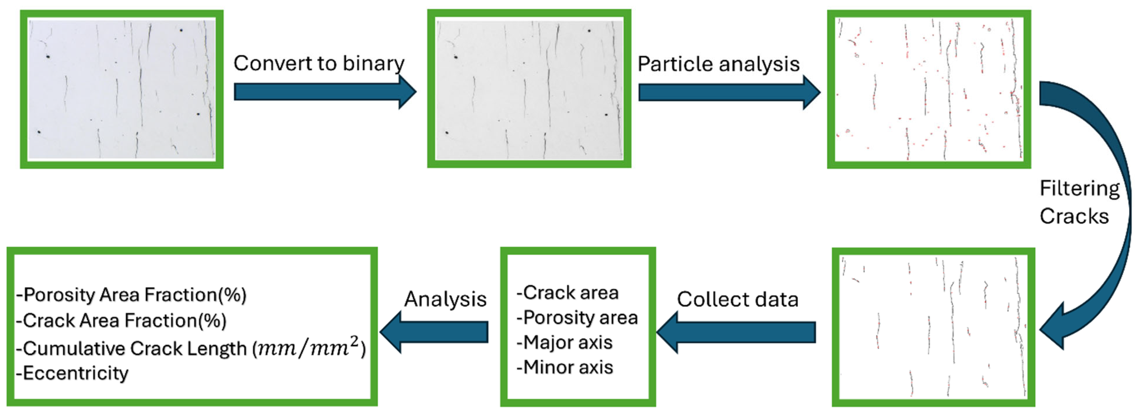
2.4. Crack Density Characterization

Image analysis of micrographs was utilized to quantify defects within the fabricated parts. ImageJ® software version1.54m was employed to differentiate micro-cracks from other defect types, including lack-of-fusion voids and keyhole pores, in the LPBF-processed samples. For each specimen, at least three polished vertical sections, located at least 0.4 mm from each other, were examined. The procedure used to statistically evaluate crack severity and porosity is illustrated in Figure 1. Quantitative data were obtained from micrographs with a field of view of 6 mm2, captured at 100× magnification, and taken at least 0.5 mm away from the sample edges. A filtration criterion of circularity <0.25 was applied to exclude voids and pores from the analysis. For each identified crack, ImageJ® was used to determine its projected area and the major axis (MA) of the ellipse fitted to the crack. Eccentricity (ECC), cumulative crack length (CCL), crack area fraction (CAF), and porosity area fraction (PAF) are calculated as follows:
E C C = 1 b 2 a 2 ,   b < a
C C L ( mm / mm 2 ) = i = 1 n M A i A i m a g e   ; M A   i s   t h e   m a j o r   a x i s   o f   t h e   e l l i p s e   f i t t e d   t o   e a c h   c r a c k
C A F ( % ) = i = 1 n A c r a c k , i A i m a g e × 100
P A F ( % ) = 1 C A F
It is noteworthy that the circularity threshold was used only to distinguish crack-like defects from pores, whereas ECC was subsequently used as a descriptor of crack morphology. The average eccentricity measured across all datasets showed a standard deviation corresponding to 0.2–3% of the mean value.

2.5. Microstructural Characterization

The surface of the coupons, as well as the as-polished cross-sections, was observed using a Keyence VHX digital microscope (KEYENCE Corporation, Osaka, Japan) to qualitatively compare the densification of samples and provide data for the crack and density quantification process explained in the previous section. After polishing the sections with colloidal silica (average particle diameter of 0.04 μm), Nital 2% was used to reveal the microstructure. Kalling’s reagent (No. 2) was used instead of Nital to obtain high-resolution pictures of dendritic microstructure in order to measure primary dendrite arm spacing (PDAS).
Electron backscatter diffraction (EBSD) was conducted to investigate the texture, grain size, and morphology, as well as the dislocation density on the YZ-section of samples. The sample preparation procedure consisted of mechanically grinding using abrasive papers up to 600 grit, followed by sequential polishing with 9, 3, and 1 μ m diamond suspensions. A final polishing step was performed by oxide polishing suspension (OPS—average particle diameter = 0.04 μ m ) to achieve a surface with minimum deformation, suitable for EBSD characterization. The EBSD analysis was performed using an FEI Versa 3D field-emission scanning electron microscope (FE-SEM) (FEI Company, Hillsboro, OR, USA) operated at an accelerating voltage of 20 keV with a 70° sample tilt and a step size of 1.1 μm. EBSD data acquisition was carried out with TSL OIM 7 software, and subsequent data analysis was performed using the AZtecCrystal EBSD version 3.3 processing suite.
Phase analysis and surface residual stress measurements were conducted using a Co-Kα radiation source with a wavelength of 1.79206 Å and a 1-mm collimator. For residual stress measurements, a 2θ angle of 124.84° corresponding to a lattice plane of 2 2 0 was employed. A total of 24 frames were acquired, consisting of eight Phi angles (0°, 45°, 90°, 135°, 180°, 225°, 270°, and 315°) and three Phi angles (10°, 27.5°, and 45°). The anisotropy factor (Arx) of the material, considered to be a nickel-based alloy, was set to 1.49 [34]. Residual stress measurements were taken on the top surface of the samples to obtain the in-plane residual stresses perpendicular to the building direction and on the side surface of coupons to represent the in-plane residual stresses along and transverse to the building direction.

3. Results

3.1. Powder Mixture Feedstock

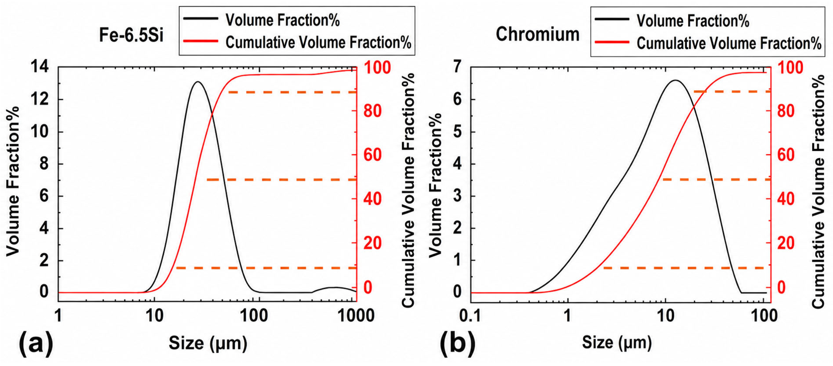
Figure 2 depicts the particle size distribution of the gas-atomized (GA) Fe–6.5Si alloy and water-atomized chromium powders.
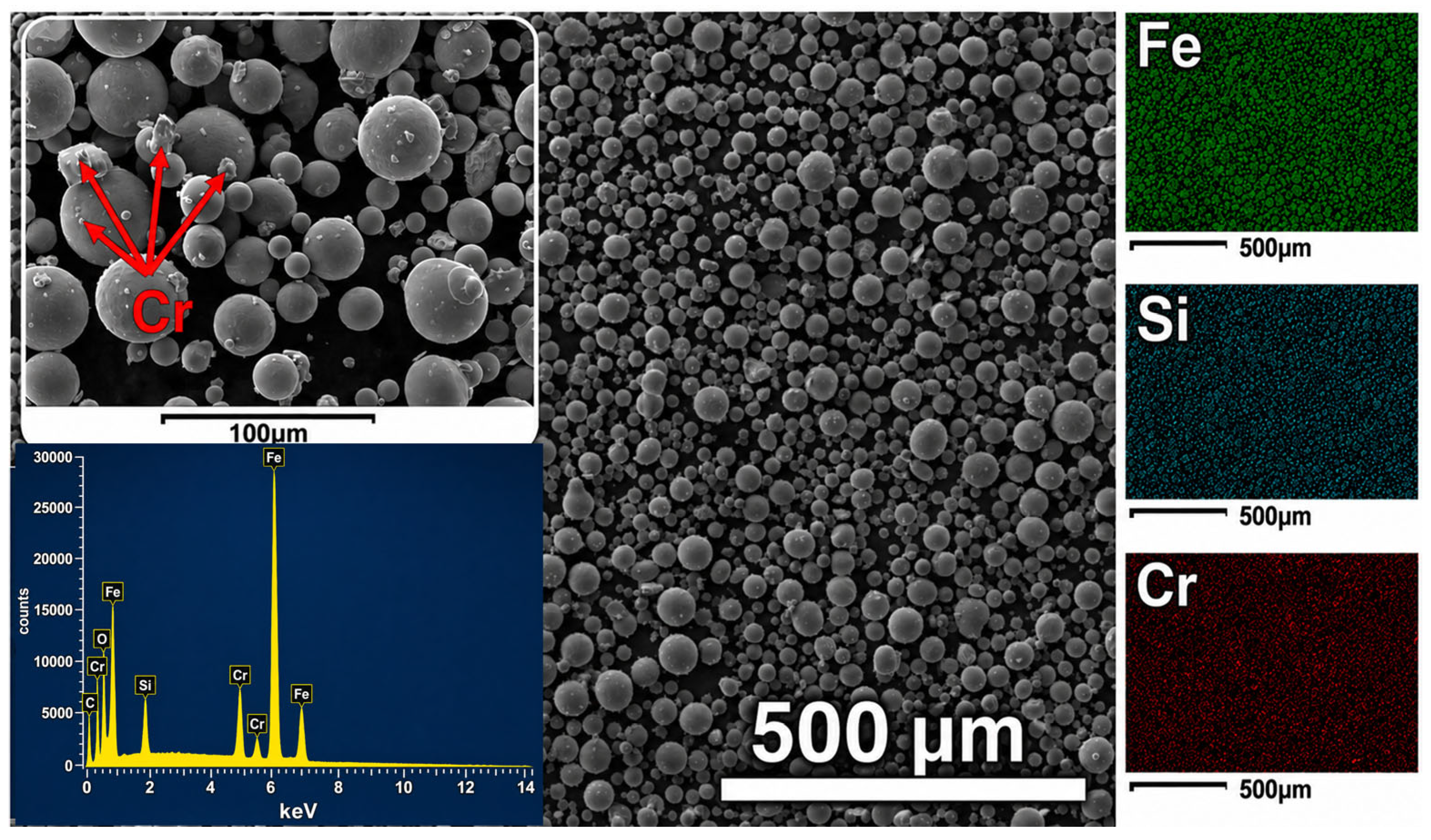
Figure 3 shows the SEM image of the prepared feedstock with 1% Cr. The almost spherical morphology of the host powder particles with their smooth surface is evident, which are both characteristics of gas-atomized powders. The finer particles of Cr powder, however, have an irregular shape. As seen, many of the fine Cr powder particles are attached to the Fe–Si powder particles, while the larger Cr powder particles are unattached to the Fe–Si powder particles and are freely distributed in between the host powder particles. The energy dispersive X-ray spectroscopy (EDS) map analysis results provided in Figure 3 confirm the relatively homogeneous distribution of Cr powder particles within the developed powder mixture.

3.2. Printability and Densification

The cubic coupons with a side length of 10 mm were printed on a non-preheated build plate. EDS analysis of specimens with reduced excitation voltage did not reveal localized Cr enrichment or discrete Cr-rich particles in the microstructure of samples processed with a sufficient level of energy, indicating a relatively homogeneous redistribution of Cr within the Fe–Si matrix after LPBF (Figure S1).
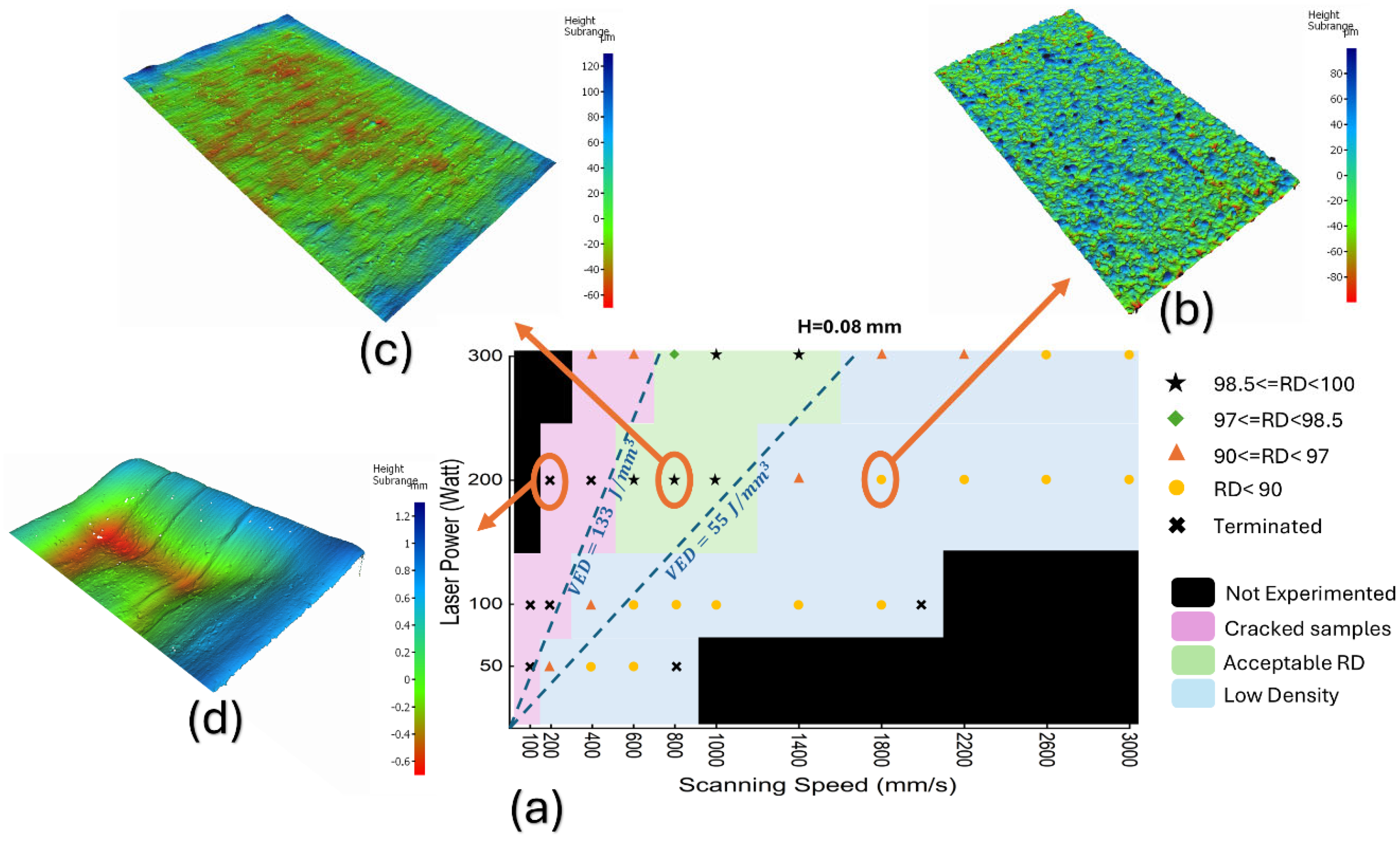
Figure 4 Depicts the variation of relative density of Fe–6.5 wt.% Si–1 wt.% Cr alloy samples processed with a hatch spacing of 0.08 mm against different laser power and scanning speed. The processing map for this alloy is categorized into four regions depicted with different colors: lack-of-fusion-dominant region, shown in blue, where the relative density is low or very low; high-and-medium-density region, colored in green, where the samples are fabricated with sufficient fusion and demonstrate the least amount of porosity and crack intensity; and the over-fused region, shown in red, where the crack intensity increases significantly, so that the relative density decreases notably and, in some cases, the sample fabrication is terminated during the process.
Volumetric energy density (VED) was used as a convenient descriptor of the nominal energy input to facilitate comparison among the processing conditions. The boundary values for volumetric energy density to define the optimum process window are 55   J / m m 3 and 133   J / m m 3 as the minimum and maximum values, respectively. However, these values for samples processed with other hatch spacings, shown in Supplementary File Figure S2, differ slightly, confirming the inefficiency of VED as a predictor parameter of the obtained relative density [11].
The printability is low in lack-of-fusion and over-fused regions, that is, many process combinations in these two areas fail to deliver a dense sample with minimal cracking, as it is observed in the process maps illustrated in Figure 4 and the ones in the Supplementary File. In previous studies, the variations in the printed layer thickness owing to unevenness and bulge on solidified layer have been found to be the cause of low densification due to porosity formation or cracking [35]. The cause of the surface bulge in the blue and red areas is different. In over-fused regions, with low scanning speed and high laser power, the continuous melt tracks can be observed clearly but there are protrusions on edges, where the tracks end and a sunken area is created just near the protruded area due to the Marangoni effect [36]. On the other hand, low volumetric energy density in the blue area resulting from low laser power and high scanning speed leads to poor wettability of the melt pool, resulting in a balling effect and discrete melt tracks [37].

3.3. Texture and Phase Analysis

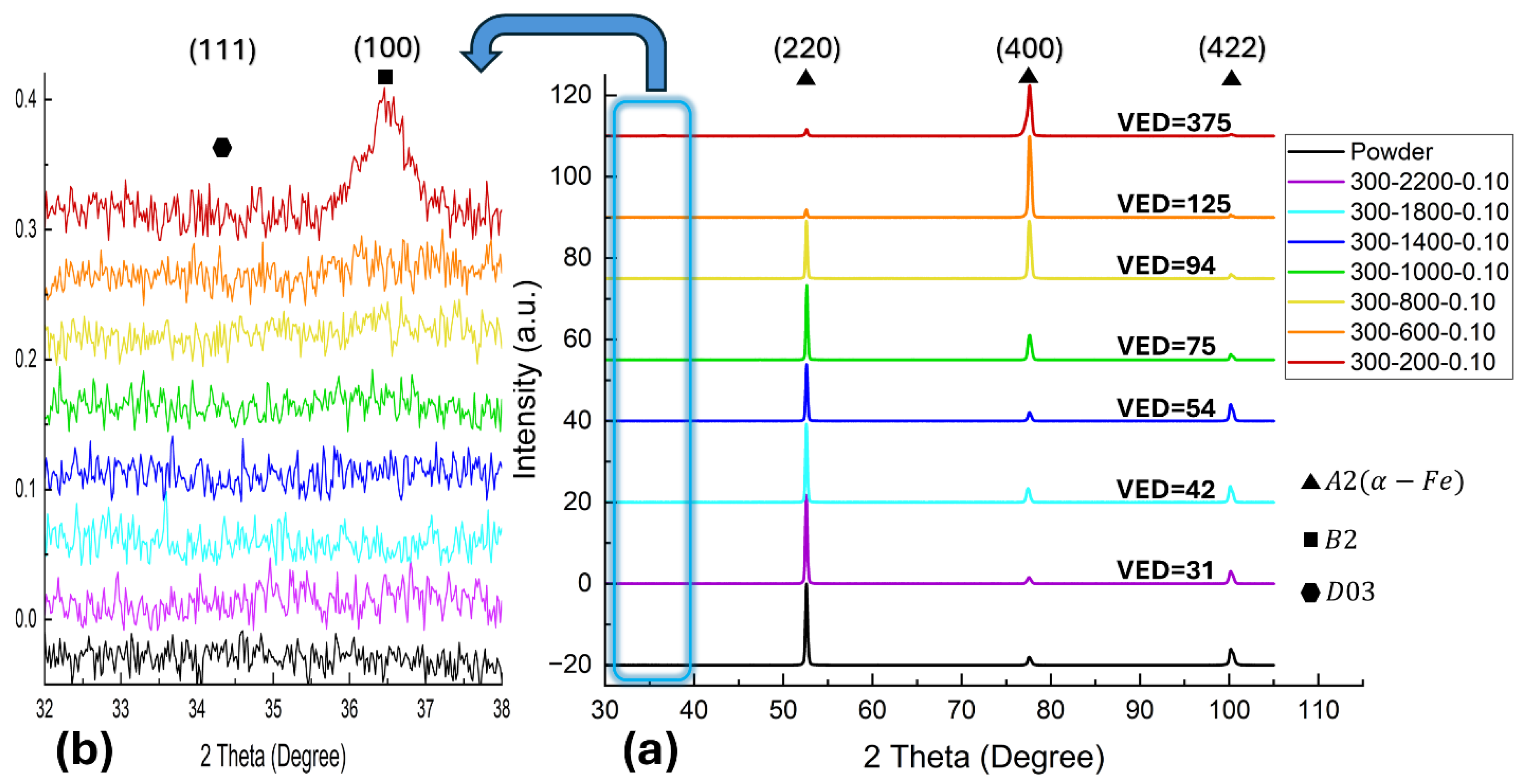
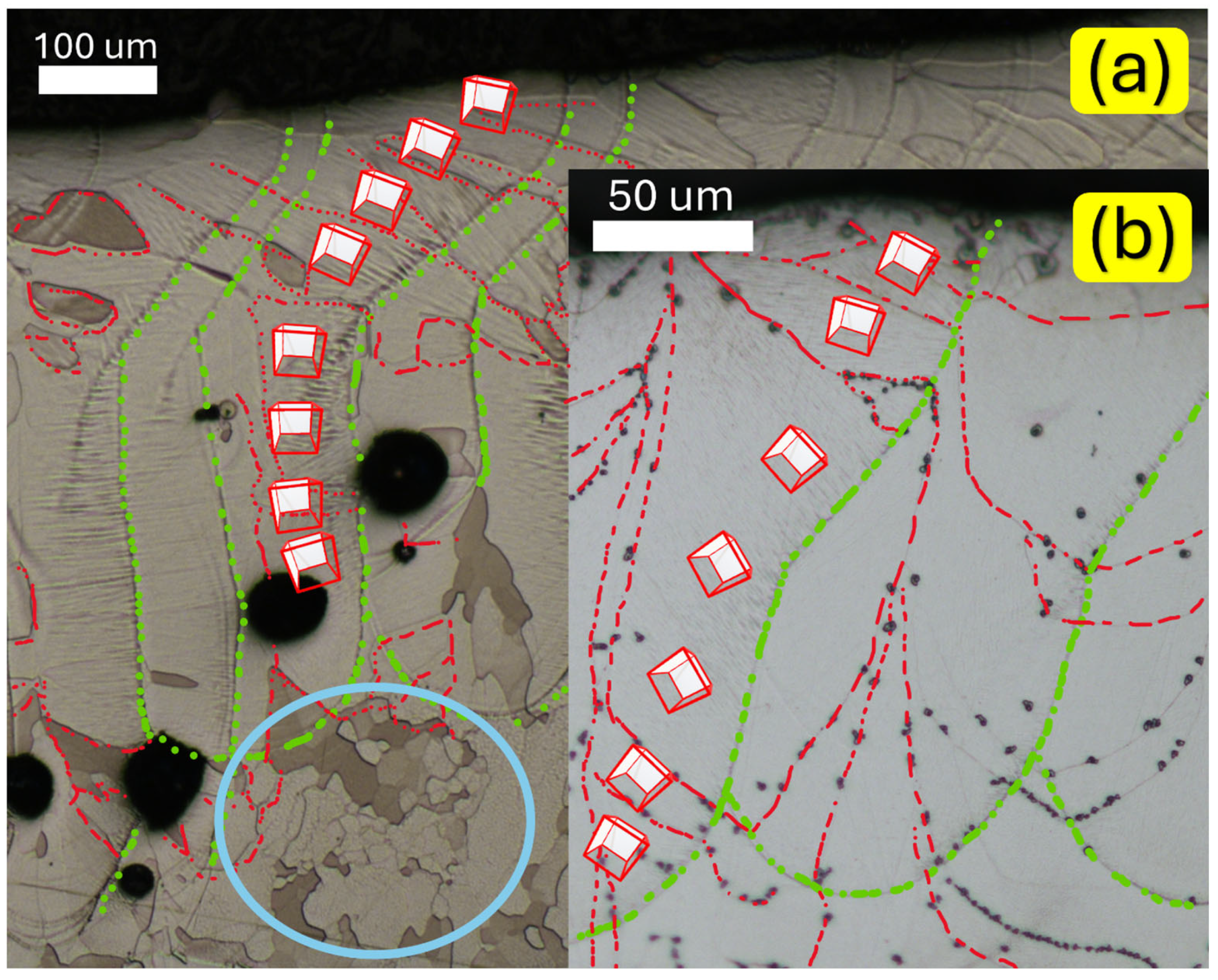
Figure 5 depicts the X-ray diffraction (XRD) spectra of powder and sections of printed Fe–6.5 wt.% Si alloy samples parallel to building direction processed at a laser power of 300 W, hatch spacing of 0.1 mm, and scanning speeds ranging from 200 mm/s up to 2200 mm/s. There are three main peaks at 2 θ =   52.6°, 78.5°, and 100.2°. The intensity of the peaks is fairly similar to the unprocessed powder with a strong peak of (220) planes at around 52.6°, until the scanning speed falls below 800 mm/s. This scanning speed is a turning point in the texture, so that the intensity of the (400) and (220) planes becomes almost equal. With slower scan speed, this trend leads to the dominance of the (400) peak in the vertical section of coupons due to changes in heat gradient and the shape of melt pools. Figure 6 compares the melt pool geometry of two samples processed with laser powers of 200 W and 300 W and identical hatch spacing and scanning speed. The microstructure and crystal orientation are mainly governed by the thermal gradient direction [38], and since the actual heat flow direction is perpendicular to the fusion line, the texture measured by XRD is abruptly influenced by the value of VED. The red-frame cubes illustrated in Figure 6 represent the crystal growth orientation of cellular or dendritic microstructure, as it is already known that the easy axis of growth in Fe–BCC is the <100> crystallographic direction [39]. In the lower section of the deep melt pool, the majority of cells grow horizontally. Therefore, one of the lattice cube’s faces opposes the melt pool boundary; hence, a significant [100] peak is traced in this sample. On the other hand, a lower fraction of cellular structure in the shallow melt pool is situated horizontally; hence, considering the hypothetical cutting surface parallel to the build direction, the intensity of the [110] peak would be much stronger than that of the [100] peak. It is worth mentioning that the vertical section studied here represents the magnetization direction in toroids, and amplification of the [100] texture would be desirable because the easy axis of magnetization in BCC structures is <100> crystallographic direction as well [40].
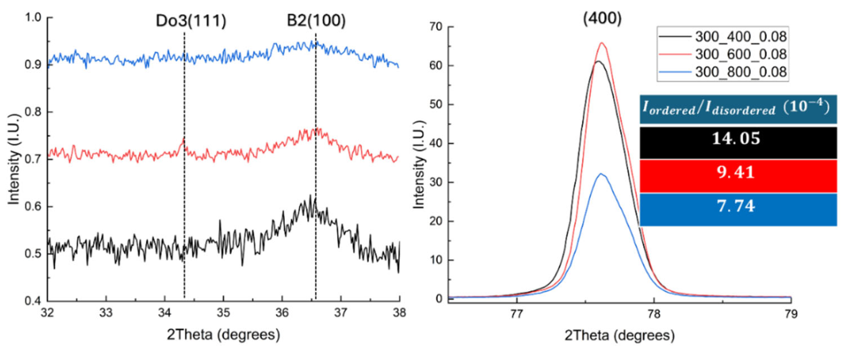
Considering the ordering phase transformation which happens in this alloy during solidification, the appearance of two identical peaks of D03- and B2-ordered phases located near 34° and 36.5°, attributed to the (111) and (100) planes of the superlattice, is expected [1]. Nonetheless, due to the rapid cooling rates inherent to the LPBF process, their formation during solidification could be suppressed [41], so that only the B2 peak is evident when the scanning speed falls below 400 mm/s. The peak of the D03 phase has hardly been detectable even in samples processed with large VEDs due to the presence of a low volume fraction of this phase, resulting from the fast cooling rate and the unfavorable texture orientation of the vertical sections for detecting this peak by XRD.
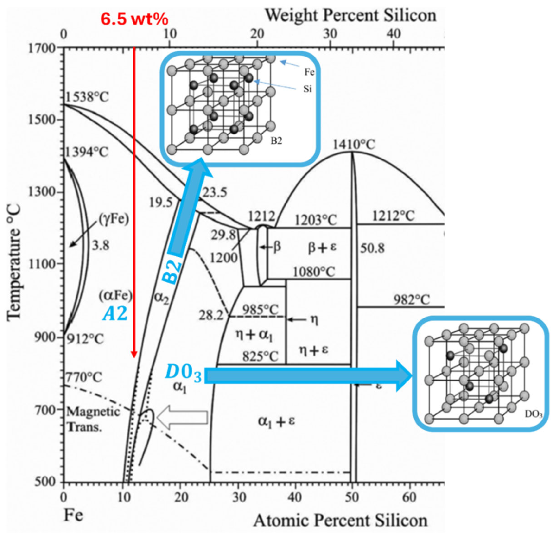
The partial phase diagram of the Fe–Si binary system is depicted in Figure 7. The solidification route of the alloy studied in this project is presented with a red arrow. Based on the stable phases shown on the phase diagram, the solidification starts at around 1450 °C, and the disordered A2 phase begins to form. With further cooling, the transition from the disordered to the B2-ordered phase occurs at around 780 °C, where the Si atoms occupy all eight center points in the superlattice. Following the cooling process, the first-order transition of B2 to D03 commences at around 650 °C through nucleation and growth [42].
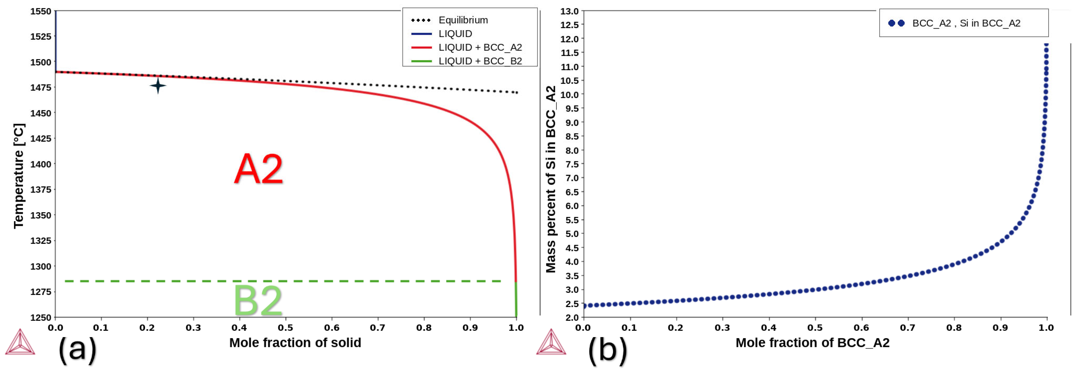
Despite the equilibrium phase diagram of the Fe–Si alloy, the actual route of solidification deviates from what is deduced from the phase diagram owing to the non-equilibrium nature of the LPBF process originating from its extremely high cooling rate. Figure 8 shows the Scheil–Gulliver solidification model of the Fe–6.5 wt.% Si alloy calculated by Thermo-Calc® software version 2024b with the assumption of fast cooling and rapid diffusion of elements in the liquid phase with no element diffusion in the solid phase [43]. As depicted, the solidification path deviates from the equilibrium condition at around 1480 °C, where the segregation of Si atoms commences. The initial solidified A2 phase has a Si concentration of about 2.5 wt.%. As solidification progresses, continued cooling drives more silicon into the remaining liquid at the dendrite growth front. Consequently, the silicon content of the solidified A2 phase rises sharply and approaches approximately 13 wt.% near the final stages of solidification. Although the phase diagram indicates that no B2-ordered phase should form at the solidus temperature, about 0.2 wt.% of the B2 phase is nevertheless produced, even under the assumed rapid cooling conditions between 1285 °C and 1255 °C.
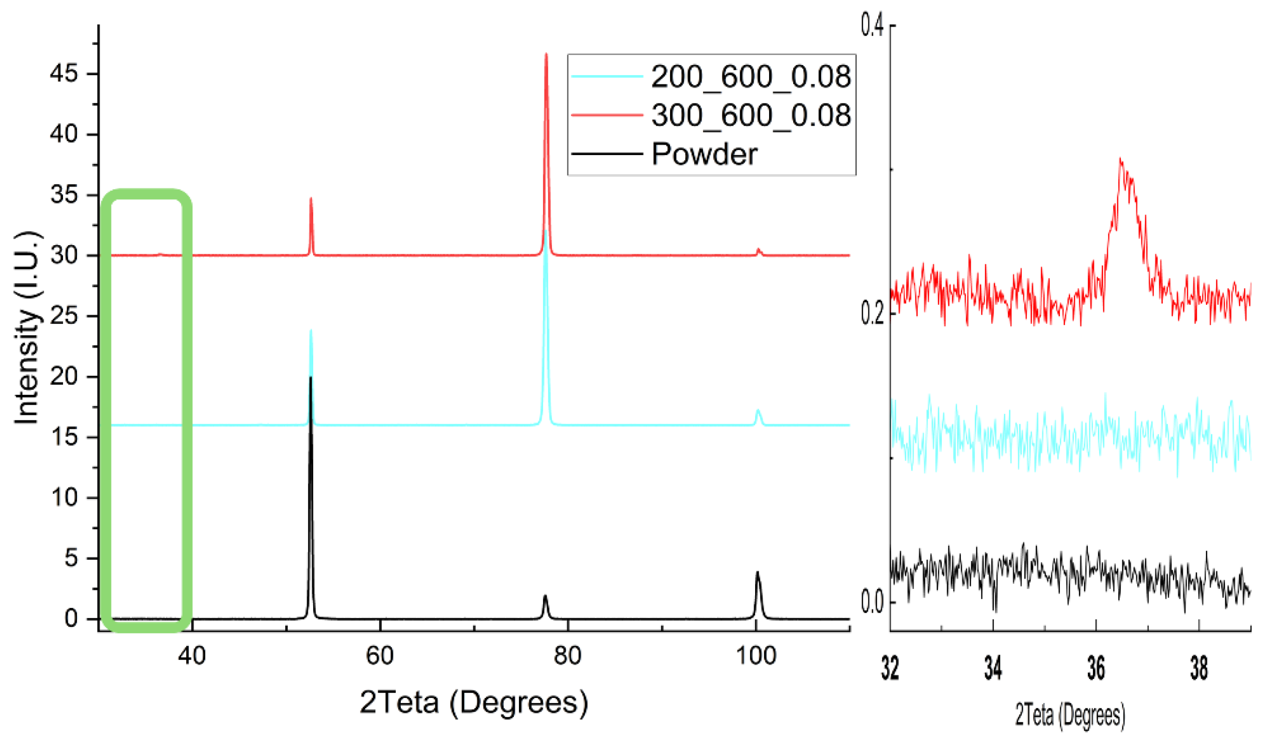
The disorder-to-order phase transformations could be bypassed via fast cooling rates associated with the LPBF process. The LPBF process is known to induce a cooling rate of 10 3 10 6 °C/s depending on the process variable combination [44], and in extreme cases, it is comparable to the cooling rate of the gas-atomization process [45]. Therefore, it is expected that no ordered phase forms via bypassing the disorder-to-order phase transformation due to rapid cooling. However, the B2 and even D03 phases were detected in some samples processed by high volumetric energy densities in this study (Figure 9 and Figure 10). XRD analysis with increased time of scan has been utilized to measure the fraction of ordered phases. The quantification is implemented by comparing the peak of B2-ordered phase (the (100) plane of superlattice peak around 37°) with the (400) peak corresponding to the similar planes in the superlattice located near 2 θ = 78°. The latter considers diffractions from the (100) planes corresponding to both disordered and ordered planes in the microstructure. As depicted in Figure 9, no ordered phase fraction is detectable in gas-atomized powder, while the B2 X-ray peak is evident in a sample processed by high laser power. The same trend applies to specimens processed by identical hatch spacing and laser powers but with various scanning speeds (Figure 10), so that lower scanning speed increases the detectable fraction of B2-ordered phase from 0.0774 vol.% at scanning speed of 800 mm/s to 0.1405 vol.% at scanning speed of 400 mm/s, which is attributed to the larger melt pool formed in lower scanning speeds that induces lower cooling rates that are not sufficient to suppress the disorder-to-order phase transformation completely [44]. This is in accordance with former findings where Viala et al. found B2-ordered phases in rapidly solidified ribbons with a cooling rate of 2 × 10 4 °C/s or higher [46]. Ouyang et al. also reported B2 and D03 phases present in melt-spun ribbons at a cooling rate of 8 × 10 5 °C/s [41]. Via modeling, it is proved that 10 6 °C/s is the critical cooling rate to avoid the formation of B2 phases [47].

3.4. Microstructural Defect Analysis

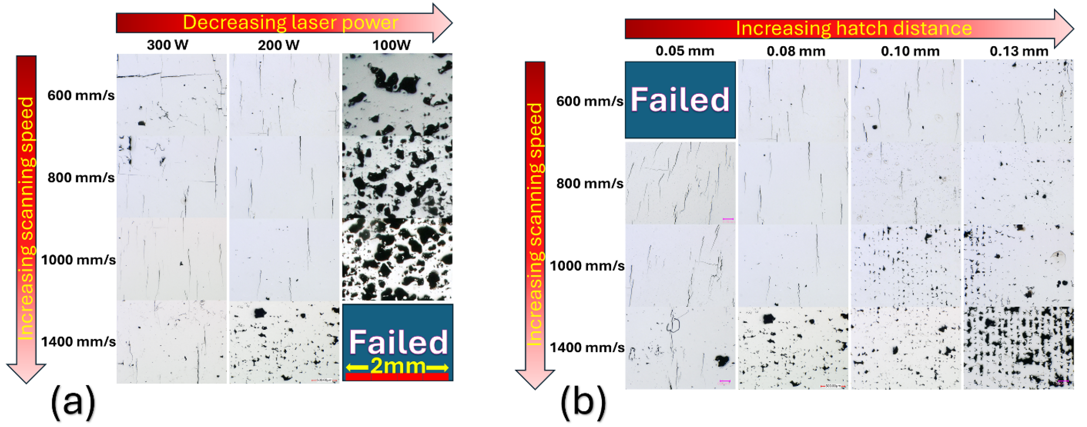
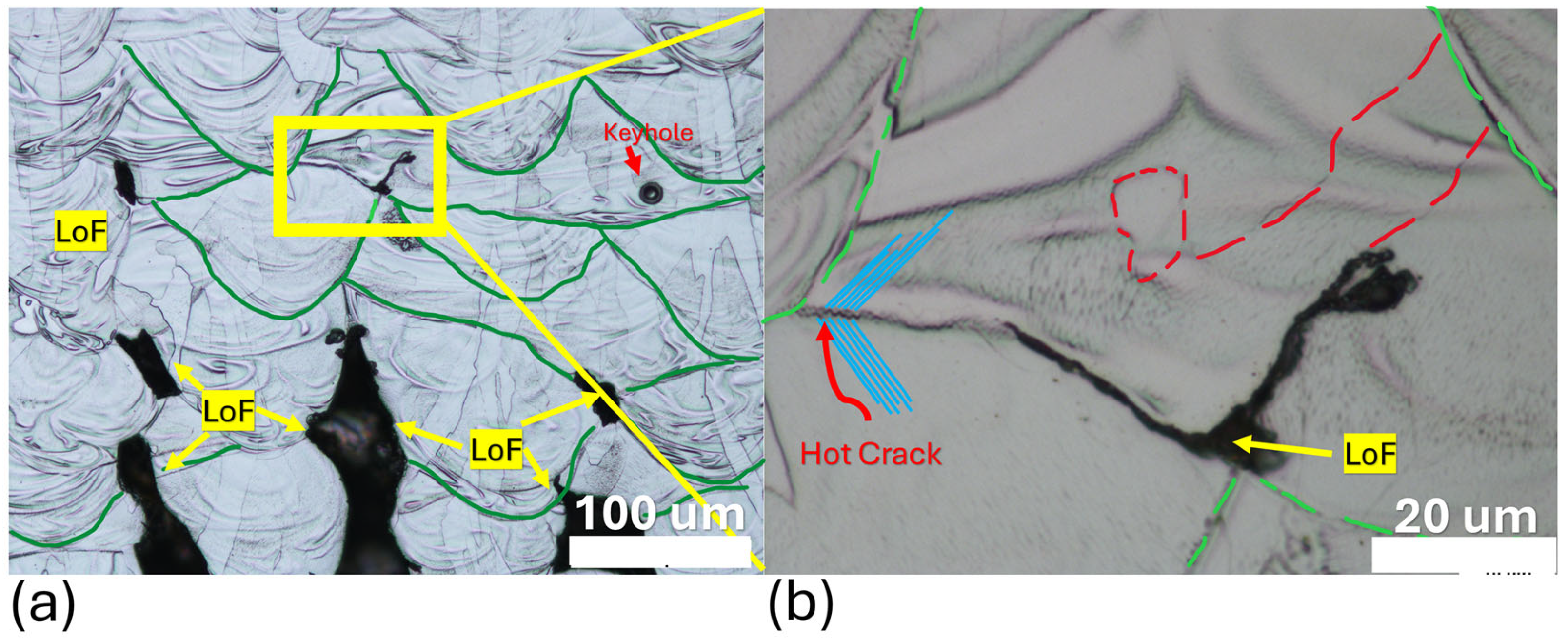
The as-polished micrographs of the LPBF-processed Fe–Si alloy samples in the as-built condition are demonstrated in Figure 11. Various types of defects exist and lead to a lower density of coupons. Spherical or semi-spherical pores observed in the microstructure are produced due to the extremely high laser energy density and consequently the keyhole phenomenon. With increased hatch spacing or scanning speed, irregularly shaped pores appear on the micrographs, and unmelted powders are present in lack-of-fusion porosities. The presence of numerous large vertical cracks is evident on fabricated samples. Some of the cracks in samples processed with low VEDs have likely initiated from the sharp edges of pores due to stress concentration (Figure 12a,b); however, the majority of cracks are confirmed to be due to the elevated energy densities. The tendency to crack in samples processed with high VEDs is attributed to the similar tendency for the brittle ordered phases to be formed in this alloy at higher VEDs, as discussed earlier. It is worth noting that melt pool boundaries have also been observed as the onset points of some cracks, similar to the former studies [22] (see Figure S2).
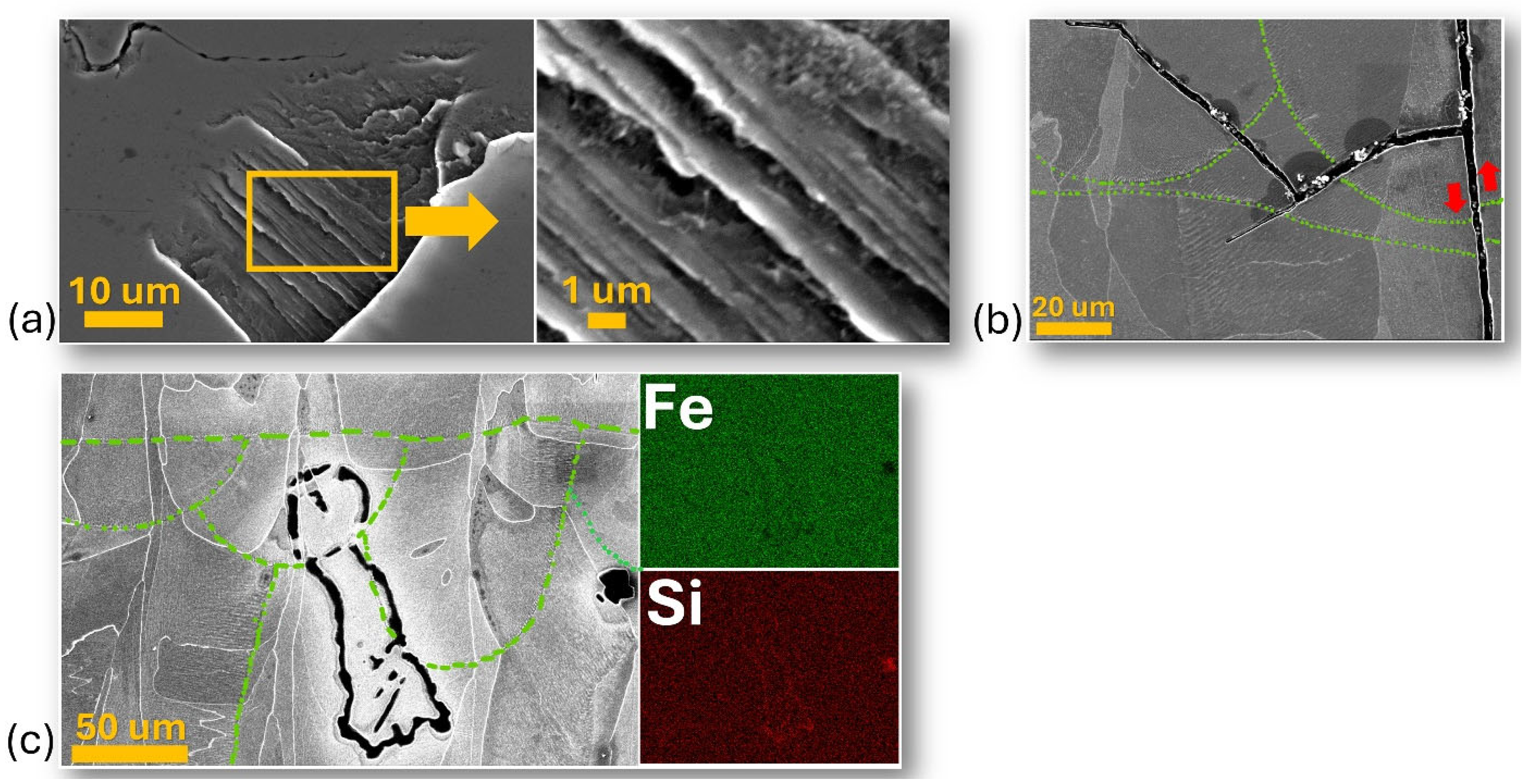
Figure 13 illustrates three kinds of cracks observed within the LPBF-processed Fe–Si alloy samples. The types of cracks could be categorized as cold cracks (also known as solid-state cracks), liquation cracks at the heat-affected zones, and solidification cracks [48]. Cold cracks develop as a result of residual stress in the solidified layers. They tend to be long, fairly straight, and transgranular, and depending on the local stress state, they may run either parallel or perpendicular to the cellular growth direction (Figure 13b). In contrast, solidification cracks have irregular, uneven surfaces. Because they form in the mushy zone during the final stages of solidification, between dendrites that have already solidified, the dendritic structure is still visible within the crack (Figure 13a). Liquation cracks, on the other hand, do not arise during primary solidification. Instead, they typically form when grain boundaries in the heat-affected zone partially remelt due to elemental segregation around the melt pools (Figure 13c).
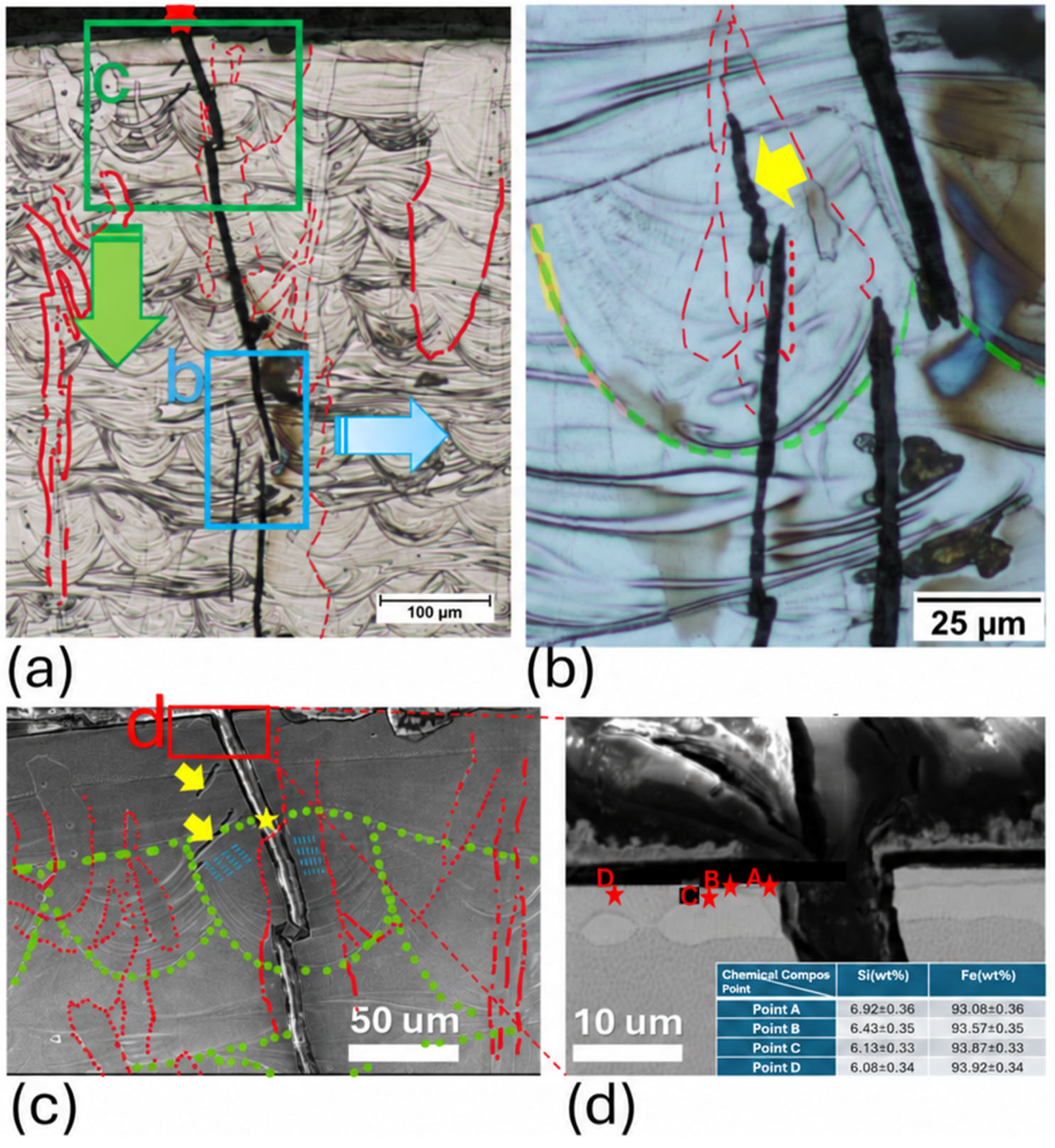
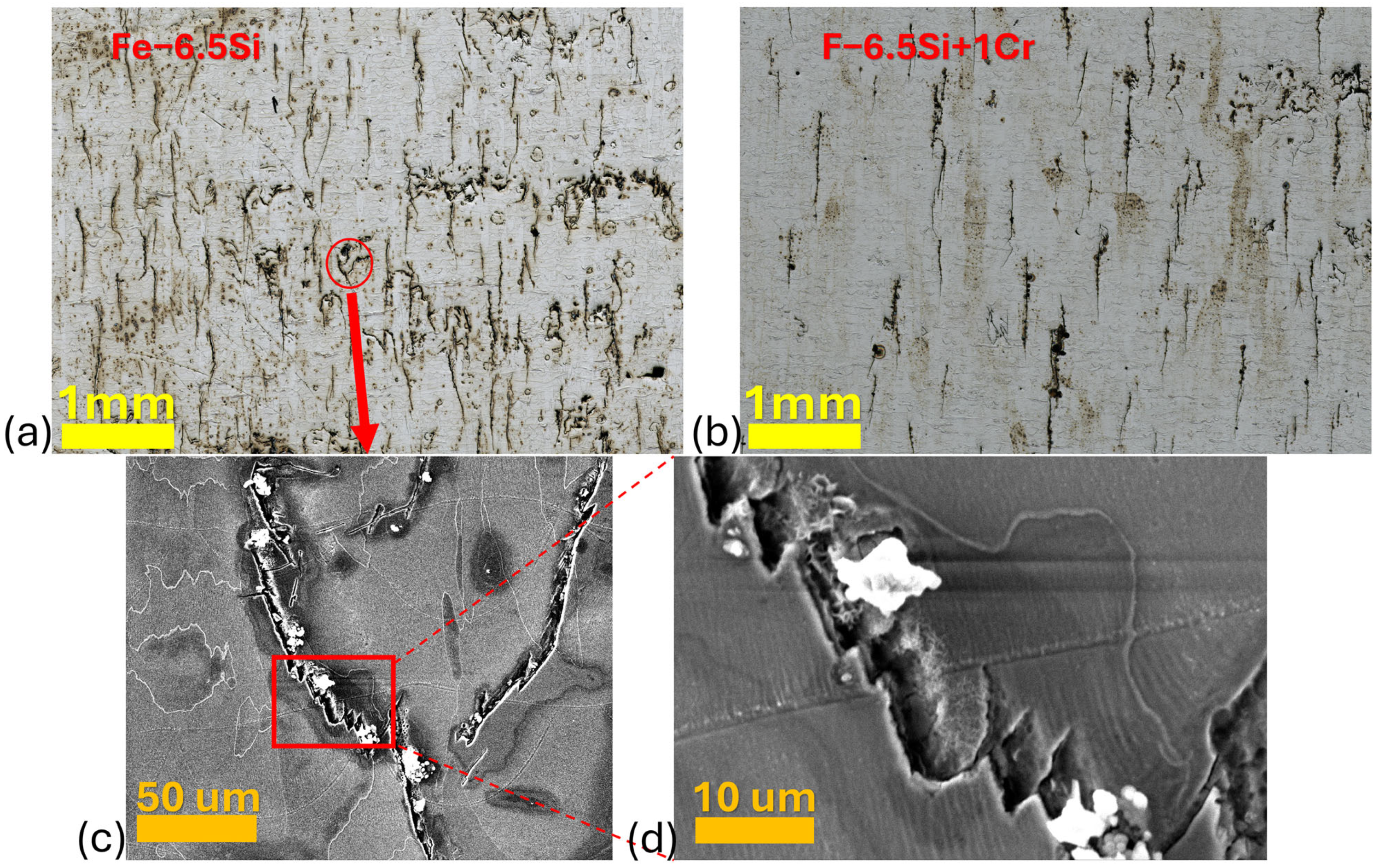
Figure 14 depicts the vertical section of a sample containing cracks. It is believed that the onset of cracks is located at a point where the residual stress exceeds the ultimate tensile strength of the alloy. The different features of solidification and solid-state cracking can be clearly observed in Figure 14. The cold crack is formed on the top surface and extends inward into the sample. The crack is transgranular with a specific direction usually resembling the directionality of cellular or dendritic microstructure inside the melt pool (dotted blue lines). On the other hand, solidification cracks are mainly observed on high-angle grain boundaries with a clear dendritic edge resembling the arms of grown dendrites. An EDS analysis with reduced excitation voltage (10 keV) was conducted near the onset of the crack to investigate the variation in the silicon content. The decreased voltage shrinks the interactive volume of the electron beam in the material to a depth of almost 500 nm [49], thus providing a satisfactory lateral resolution to demonstrate elemental variations. The silicon concentration decreases from 6.92 wt.% just beside the crack to around 6 wt.% at a point 10 μ m distant from the crack. This variation in silicon content due to the segregation of silicon promoted the formation of a brittle ordered phase on the top layer with elevated residual stresses which initiated the crack.
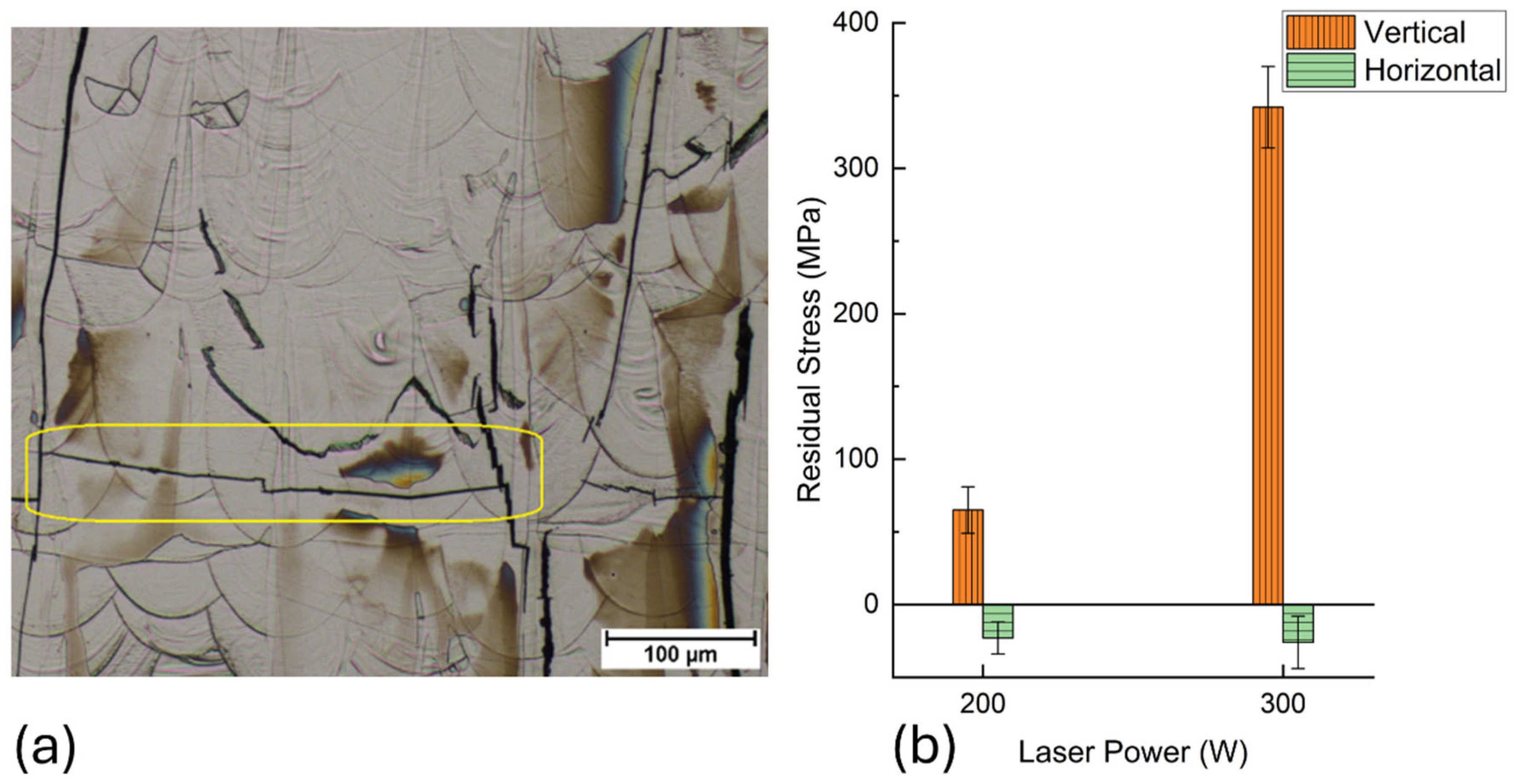
The crack directions in samples with a laser power of 100 W or 200 W are parallel to or highly in line with the building direction. However, when the sample is processed by a laser power of 300 W, numerous horizontal cracks appear on the cross-section. The solidification structure is largely influenced by the direction of heat flow as the melt pool cools, with grains typically growing in line with this thermal gradient [38]. In LPBF, the low thermal conductivity of the surrounding powder causes heat to dissipate primarily downward through the already-solidified layers of the part to the build plate. As a result, grains tend to grow epitaxially along the building direction. For alloys with a body-centered cubic (BCC) crystal structure like Fe–Si, the preferred growth direction is along the <001> crystallographic axis [39]. Because grains oriented in the <100> direction grow more rapidly than those in other orientations, columnar grains aligned with the build direction are formed. However, the actual path of heat flow is also affected by the melt pool’s geometry and the curvature of its boundaries. In cases where lower or moderate laser power creates shallow melt pools, grain growth tends to follow the contour of the melt pool, growing roughly perpendicular to its curved boundary across successive layers. On the other hand, when high laser power generates a deeper melt pool, the grain growth direction is nearly horizontal but gradually shifts to align with the vertical build direction. This gradual deviation in crystal growth orientation forms horizontal or near-horizontal high-angle grain boundaries, where due to the high VED applied, the segregation of silicon intensifies, leading to the formation of brittle ordered phases along the high-angle grains. In addition, while the residual stresses in samples processed by low and medium laser power are notable perpendicular to the melt tracks, the highest level of residual stresses is along the building direction in samples fabricated by elevated laser power. Therefore, a horizontal microcrack could initiate on the semi-horizontal grain boundaries or along the substructure growth orientation, which then propagates horizontally or at an angle as a solid-state crack perpendicular to the direction of residual stress. In addition, with high laser power, the size of the melt pool and heat-affected zone (HAZ) increase significantly; hence, the chance for liquation cracking just beneath the melt pool boundaries (fusion lines) increases (see Figure 15).

3.5. Crack Intensity as a Factor of Process Variables

The effect of the process parameters on the formation of microstructural defects was examined. When the VED is reduced, whether by lowering the laser power, increasing the scan speed, or widening the hatch spacing, lack-of-fusion pores become more common, while most cracks disappear. In contrast, raising the VED results in a higher crack density. At sufficiently high VED levels, the alloy also develops round, keyhole-type pores during processing.
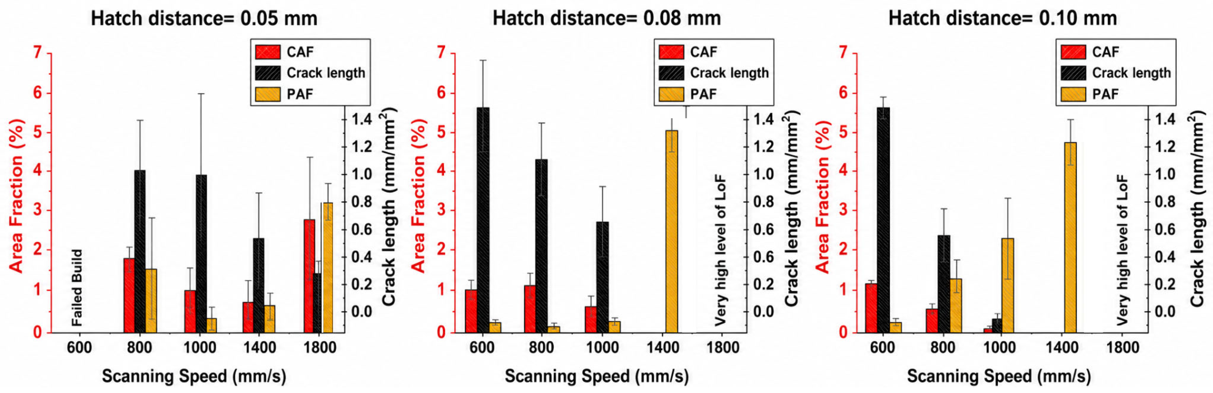
Figure 16 shows the number of defects classified as either cracks or pores in the samples built with 200 W laser power under different hatch spacings and scan speeds. Samples produced with a 0.05 mm hatch spacing exhibit extensive cracking, and most of their discontinuities are crack-related. In contrast, when the hatch spacing is increased, pores account for the majority of the defects. Looking at both the cumulative crack length (CCL) and the crack area fraction (CAF), a clear trend appears. Increasing the hatch spacing from 0.05 mm to 0.10 mm reduces the CAF but increases the CCL, indicating that the cracks become narrower as the hatch spacing is increased.
The B2 and D03 ordered phases are known to make Si-rich steels more brittle. Their presence reduces ductility because they hinder normal dislocation motion. In the disordered A2 structure, dislocation slip does not disturb the arrangement of Fe and Si atoms, so no antiphase boundary is produced. In contrast, deformation in fully ordered B2 or D03 phases requires the movement of “super” dislocations, pairs of dislocations in B2 and sets of four in D03, which involves creating antiphase domain boundaries. Because this mechanism demands a precise and coordinated movement of multiple dislocations, slip is more difficult, and the material becomes more brittle [17]. Given that more ordered phases were found in samples processed at higher VED, the increased cracking observed at higher laser powers or lower scan speeds is consistent with the larger fraction of brittle ordered phases.

3.6. Effect of Doping Element

The role of added Cr on the solidification path and crack susceptibility of the Fe–6.5Si alloy has been investigated in this section with a combination of experimental analysis and thermodynamic simulations.
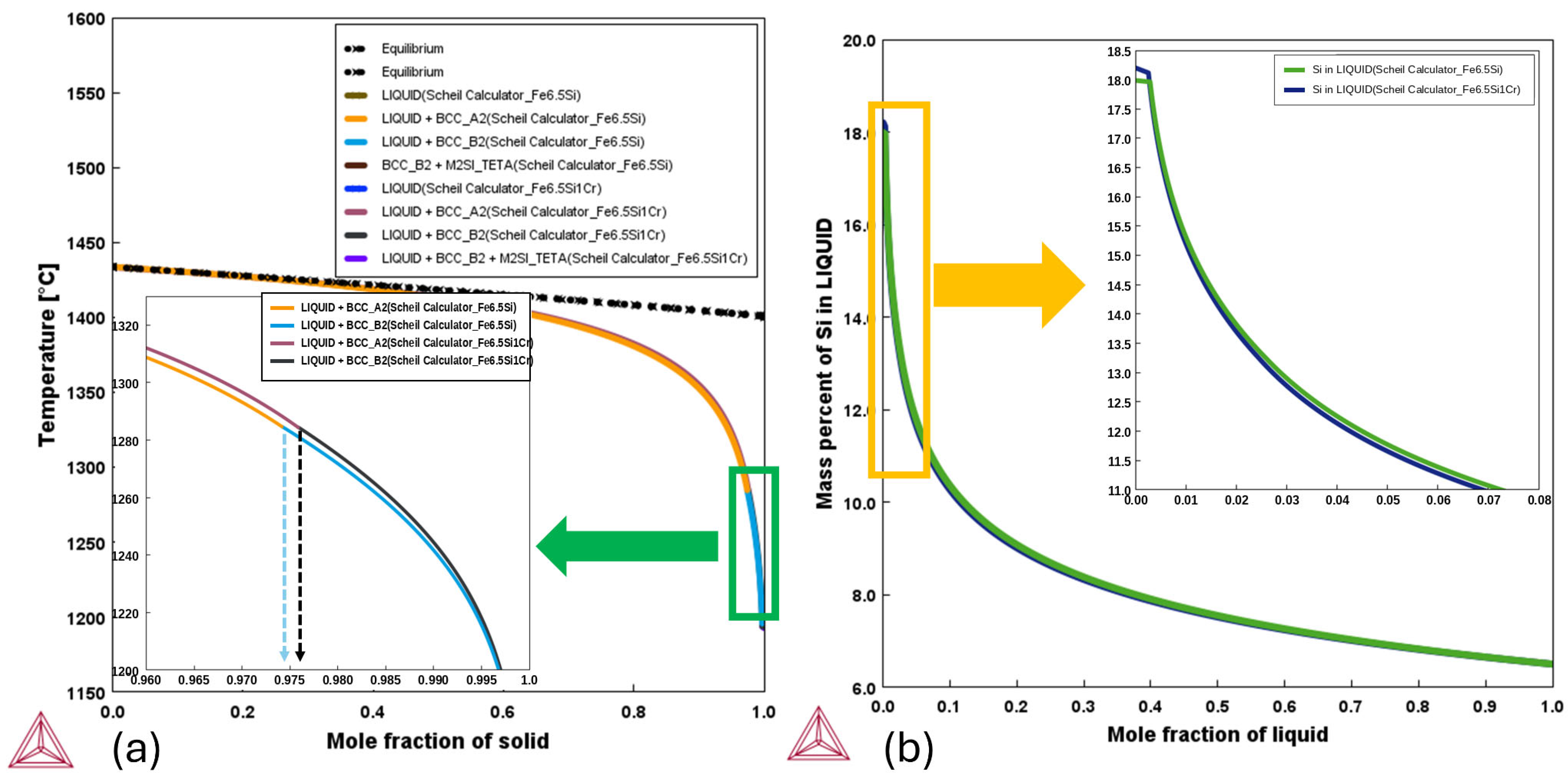
Figure 17a illustrates the Scheil–Gulliver simulation of the solidification route of Fe–6.5Si and Fe–6.5Si–1Cr alloys. As evident, both alloys deviate from the equilibrium path at around 1427 °C, when almost 22% of liquid is solidified; then the solidification continues until all the liquid transforms into solid. With careful consideration of the diagram, it is revealed that the alloy without Cr deviates from the equilibrium solidification path more than the alloy with added Cr does. Moreover, it is inferred from the diagram that transformation from liquid to the ordered B2 phase starts slightly later in the alloy containing 1 wt.% Cr, meaning that there are less ordered phase forms during the solidification of the melt pool. Figure 17b confirms those findings by plotting the evolution of Si concentration in the remaining liquid during solidification versus temperature in these two alloys. Both alloys experience a similar upward trend, indicating that as solidification proceeds and liquid fraction reduces, the concentration of Si in the remaining liquid increases exponentially due to rejection from the solid. The green and black curves are very close to each other, but the Cr-containing alloy (black) has slightly less silicon concentration in liquid, which suggests Cr subtly influences the partitioning behavior in the liquid and suppresses early Si-enrichment in the melt pool, which can end up in less brittle ordered phases.
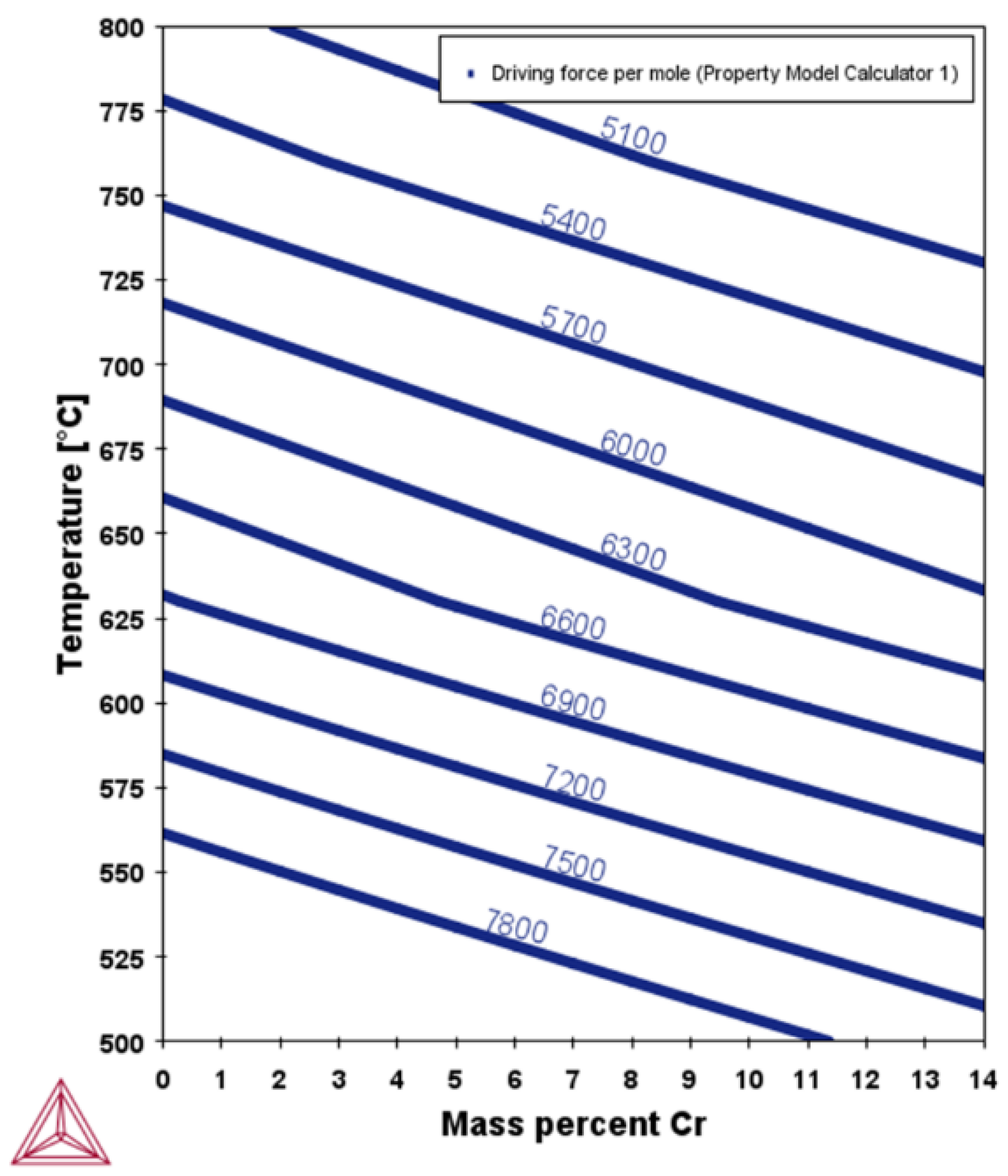
The influence of Cr on suppressing the formation of ordered phases via reducing the segregation of Si in melt pool is not limited to the liquid-to-solid phase transformation stage but continues at temperatures lower than the solidus line and acts in favor of stabilizing the A2 disordered phase. Figure 18 demonstrates the driving force for the formation of 1 mole of B2-ordered phase against various temperatures. As evident, addition of even 1 wt.% Cr to the composition lowers the driving force for disorder-to-order phase transformation in all the temperature range calculated here. In other words, Cr helps sustain a larger fraction of disordered phase in the microstructure.
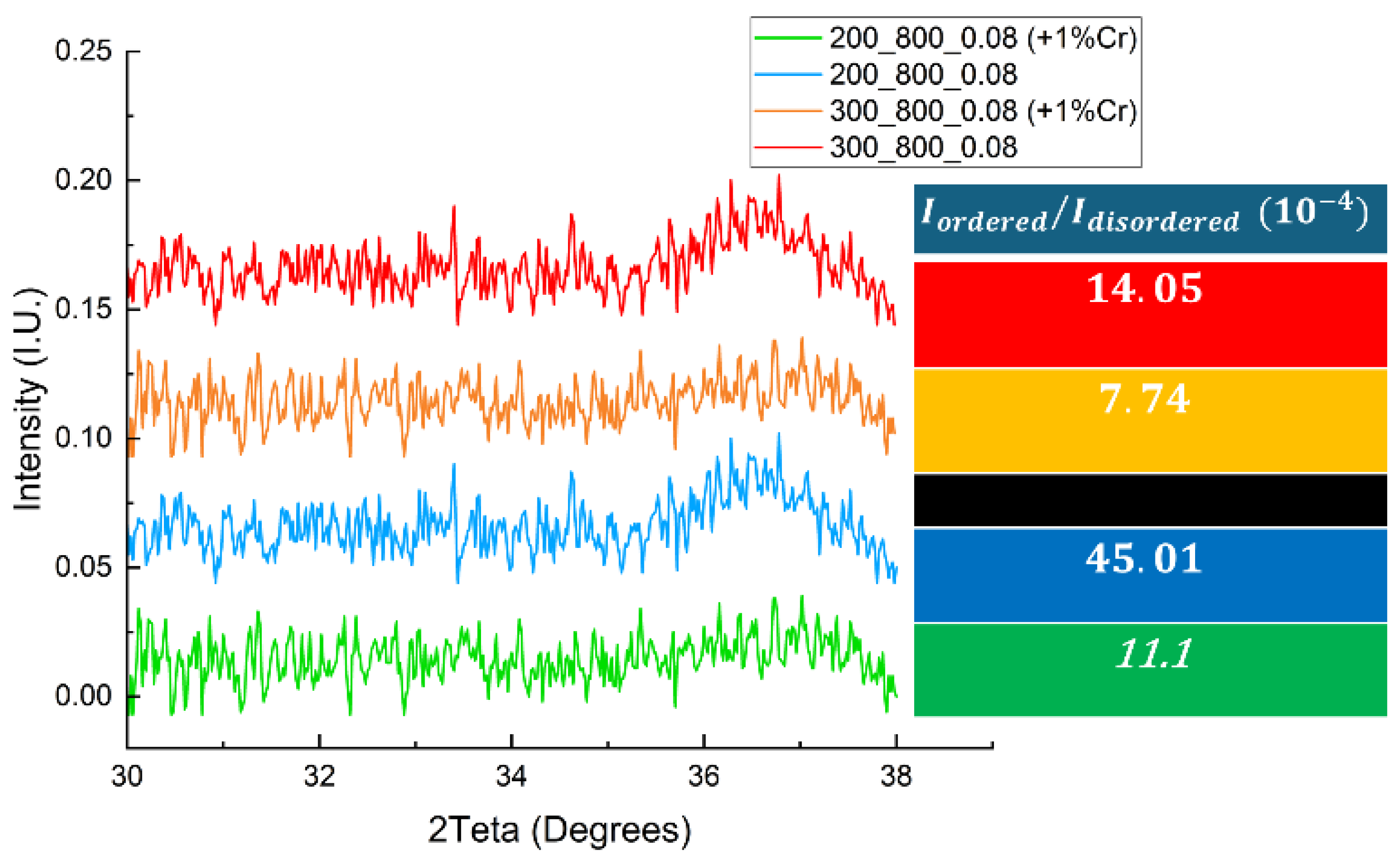
The experimental findings also highlight the beneficial effect of adding chromium on limiting the development of ordered phases. Figure 19 shows the XRD patterns for Fe–6.5Si and Fe–6.5Si–1Cr samples processed with two different parameter sets. For each spectrum, the intensity ratio of the B2 ordered peak to the (400) peak is calculated and noted. In the Fe–6.5Si samples produced with high and medium laser powers, this ratio is roughly twice and four times higher, respectively, than in the Cr-alloyed samples. This clear reduction demonstrates that chromium effectively suppresses the ordering transition.
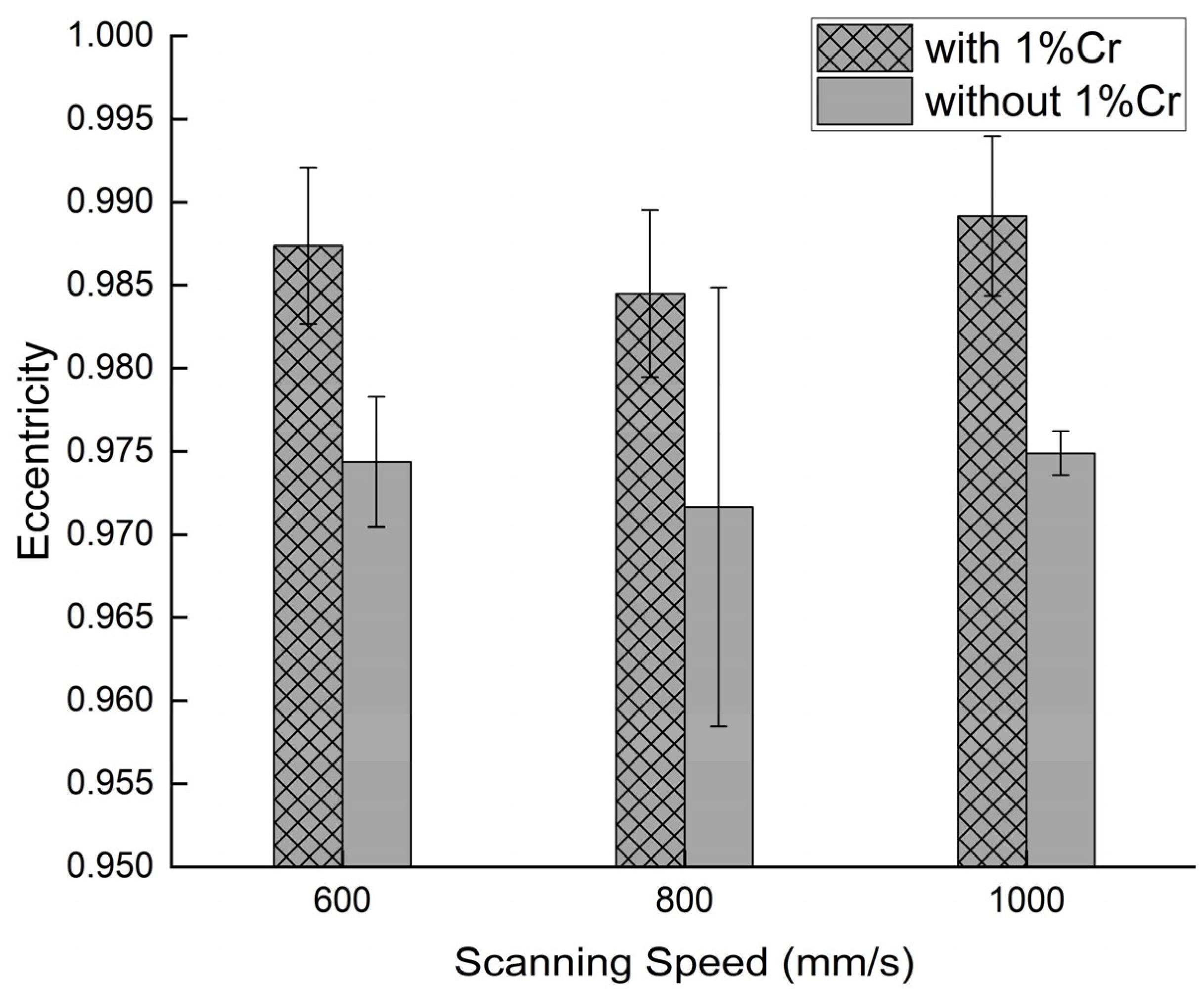
The effect of adding 1 wt.% chromium to the Fe–6.5 wt.% Si alloy could be realized from the cross-sectional optical micrograph of samples made of feedstock with and without Cr, portrayed in Figure 20. The sample without Cr contains more cracks and many of them are categorized as liquation and solidification cracks with obvious dendritic features (Figure 20c,d), while the sample made of Cr-doped feedstock has a lower crack density, with the majority of them straight, categorized as solid-state cracks. Comparing the morphology of cracks on samples could be utilized as a hint to investigate the dominant cracking criteria on fabricated samples. As a crack morphology quantifier, the micro-crack eccentricity is defined as a function of major (a) and minor (b) axes of the crack [50]. A higher value of ECC, calculated by formula 1, represents a straighter crack morphology and, when considered together with the microscopic observations, indicates a greater contribution of solid-state cracking relative to the more irregular solidification and liquation cracks.
The ECC value of samples made of the alloy with and without added chromium is depicted in Figure 21. The samples containing chromium have a significantly higher ECC value which proves that fewer oval-shaped cracks are present on the studied surfaces and most of the cracks are straight. This means the dominant mechanism of cracking in the chromium-containing alloy is solid-state cracking, while in the alloy without Cr, it is solidification or liquation cracking. The results of ordering intensity shown in Figure 19 support these findings. With the addition of 1 wt.% chromium, the intensity ratio of the ordered peak to the disordered peak has decreased almost four times at a laser power of 200 W and two times when the samples are processed by a laser power of 300 W. Lower presence of ordered phases in alloy with 1% chromium aligns well with the less frequent solidification and liquation cracking morphology, because both phenomena stem from the segregation of silicon during solidification. In other words, addition of 1 wt.% chromium is very significant in suppressing the segregation of silicon during cooling and helps to achieve a smaller fraction of ordered phases and diminishes solidification and liquation cracks, simultaneously. These results are in agreement with former findings from another study that showed added Cr reduced the ordering tendency in casting Fe–6.5Si alloy [26].
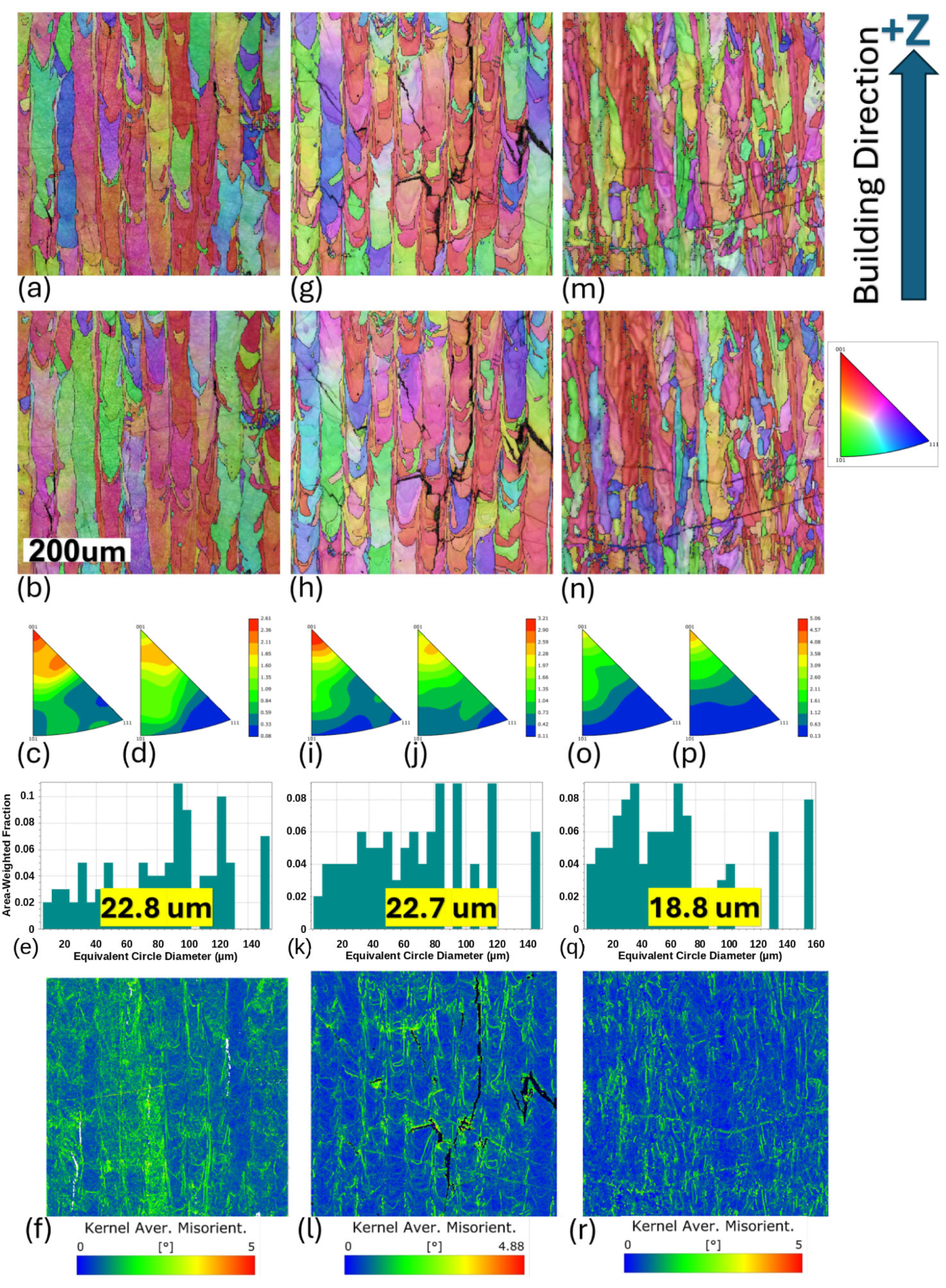
Figure 22 depicts the EBSD results of samples made of Fe–6.5 wt.% Si and Fe–6.5 wt.% Si–1 wt.% Cr alloys. The addition of chromium to the Fe–6.5 wt.% Si alloy produced a clear grain-refinement effect: EBSD quantification shows a higher population of small grains in the Fe–6.5 wt.% Si–1 wt.% Cr alloy compared with the Cr-free condition (Figure 22e,k). This behavior is consistent with the well-known role of Cr as an accelerator of grain nucleation [28,32,51]. The finer grain structure developed in the Fe–6.5 wt.% Si–1 wt.% Cr alloy likely plays a key role in reducing the formation of cracks. Grain refinement increases the volume fraction of grain boundaries, which can interrupt crack propagation and serve as effective sites for stress redistribution. These interfaces also allow limited grain-boundary sliding and localized plastic accommodation, helping the material to better withstand thermal stresses generated during solidification and cooling. Kernel average misorientation graphs (Figure 22f,l) demonstrate significantly lower lattice misorientation in the sample with Cr compared to the one without Cr, affirming the role of Cr in reducing lattice misorientation and crack initiation.

3.7. Effect of Build Preheating

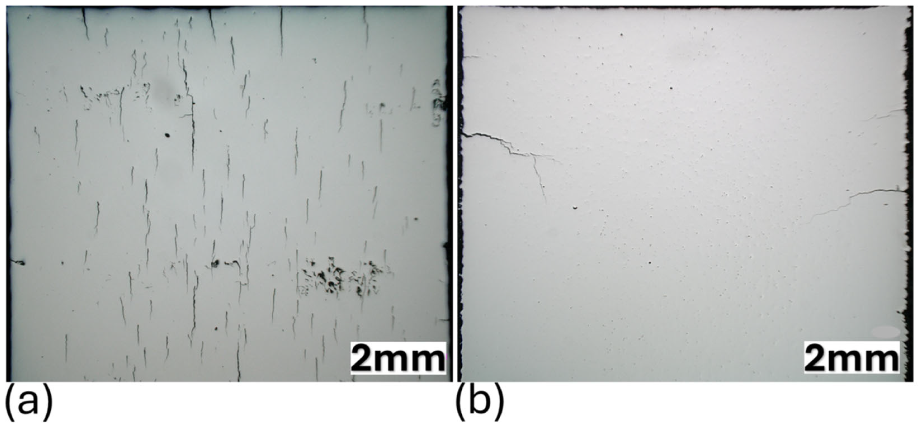
Figure 23 presents the microstructures of Fe–6.5 wt.% Si–1 wt.% Cr specimens produced with and without build preheating. In the sample fabricated without preheating, numerous vertical cracks can be seen, typically extending in the build direction and cutting across several layers. Such cracks are indicative of high thermal stress generated during rapid solidification, which, combined with the limited ductility of high-silicon iron alloys, tends to cause intragranular failure. By contrast, the preheated build shows a dense and continuous structure without visible vertical cracking, but numerous tiny pores are evenly distributed. The application of preheating eliminated the vertical cracks, though a few edge delaminations persisted, probably due to stress concentration near the specimen boundaries. These edge defects may be associated with a redistribution of the residual-stress state under preheated conditions, where thermal expansion and contraction remain constrained by the surrounding material and the build substrate. Previous research has similarly reported an accumulation of residual stress parallel to the build direction near the specimen perimeters [52].
Referring to Figure 22, when the build platform is not preheated, the EBSD IPF-Z map shows a distinctly columnar grain structure aligned with the build direction, where elongated grains extend across multiple layers. Pronounced vertical cracks are evident between these columns, indicating the presence of high residual stresses and limited plastic accommodation during solidification. The observed grain morphology points to a predominance of epitaxial growth, which is typical for LPBF processing under steep thermal gradients. When the build preheat was raised to 200 °C, the microstructure changed noticeably, becoming more uniform and less columnar. The grains appeared shorter and more equiaxed, reflecting a modification of the solidification behavior. This finer and more isotropic morphology suggests that preheating reduced the thermal gradient between the melt pool and the previously solidified layers, thereby suppressing directional grain growth along the building direction. The area-weighted grain size histogram provided in Figure 22e,k,q supports these observations: at 200 °C, the distribution becomes narrower, with a higher proportion of medium-sized grains (20–80 µm) and fewer large grains exceeding 120 µm. This indicates that preheating not only refined the average grain size but also promoted greater microstructural homogeneity. Additionally, the absence of vertical cracks at the 200 °C condition highlights the beneficial role of preheating in relieving thermal stress. The combination of finer grains and reduced anisotropy likely enhances strain accommodation and suppresses the vertical crack population; however, a limited number of horizontal cracks initiated from edges remained after preheating.
Comparison of the IPF-Z texture plots of the samples shown in Figure 22 indicates no substantial variation in crystallographic orientation along the build direction. In all cases, most grains are aligned with the build direction (<100>) or oriented between the <100> and <102> directions, resulting in largely similar texture patterns. The prevalence of the <100> orientation is consistent with previous reports [44], which identify <100> as the preferred growth direction in body-centered cubic (bcc) crystal structures.
A more detailed examination of the IPF maps taken perpendicular to the analyzed sections highlights the influence of chromium addition and build-plate preheating on the crystallographic texture normal to the vertical faces of the cubic samples, corresponding to the magnetization direction in toroidal components. Figure 22d,j,p presents the texture plots perpendicular to the vertical sections for samples without Cr, with Cr, and with Cr processed under elevated build preheat, respectively. The texture intensity of the direction of <100> as the easy magnetization axis is ~1.47 in the Cr-free sample and increases to approximately 1.71 with the addition of Cr. Notably, this intensity further rises to 3.8 when the Cr-containing sample is fabricated at elevated build temperature, demonstrating the effectiveness of build preheating in promoting grain alignment perpendicular to the build direction. In other words, in the Cr-modified sample processed at 200 °C, the columnar grains exhibit minimal rotation around the Z-axis, with lattice planes remaining largely parallel to the examined section. In contrast, samples fabricated at 30 °C show a tendency for grain rotation around the Z-axis, leading to a noticeable <101> component in their texture distributions.

3.8. Effect of Sacrificial Wall Around the Part on Cracking Mitigation

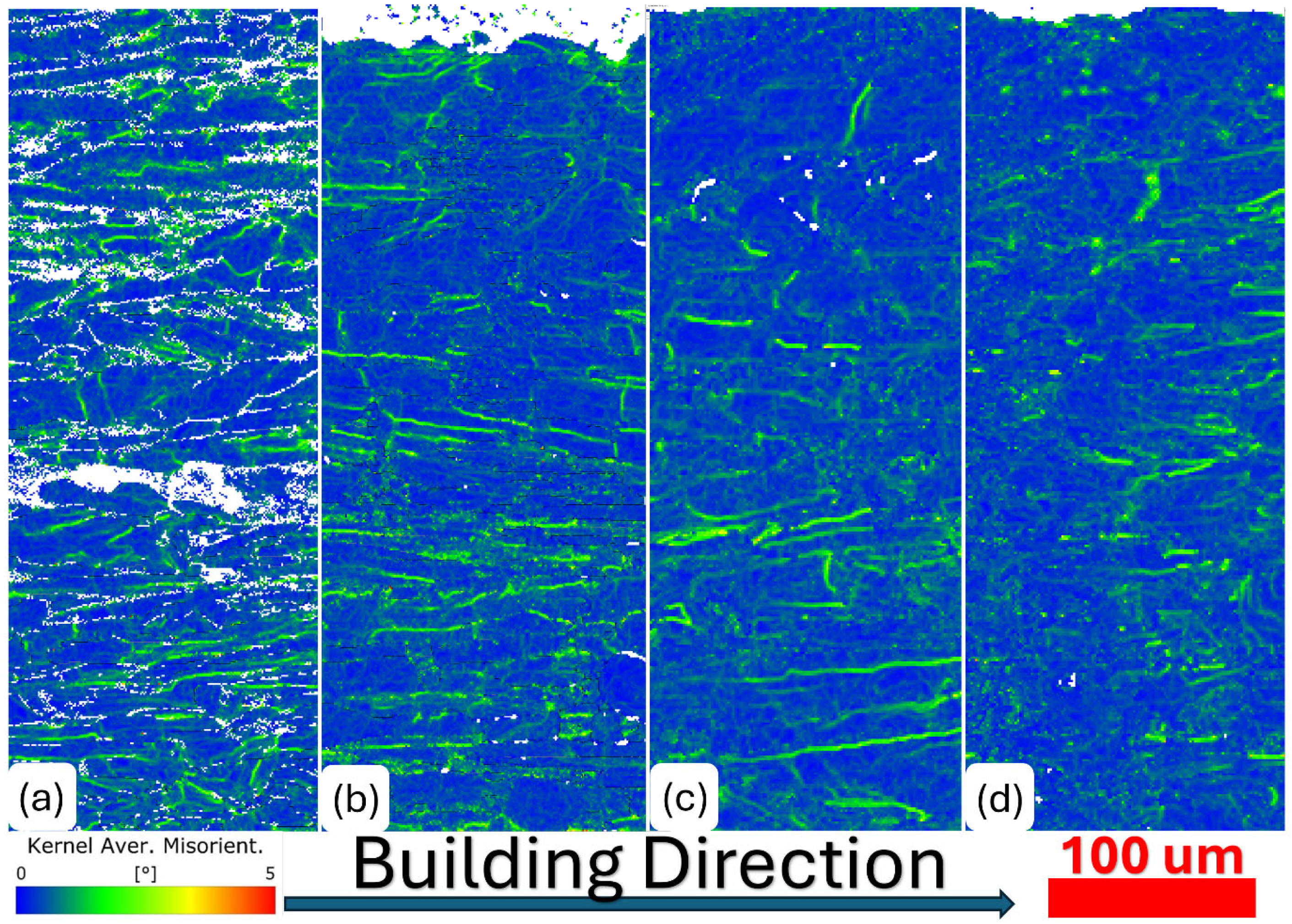
When coupons were printed on a preheated build plate, horizontal cracks initiated at the sample edge and propagated toward the interior. Similar behavior has been reported in LPBF processing of other alloys with high crack sensitivity, where elevated platform temperatures substantially reduced cracking, but occasional horizontal cracks persisted near specimen edges due to locally high thermal gradients [53]. To mitigate the pronounced thermal gradients and high cooling rates at the part edges that contribute to edge cracking, thin sacrificial walls were printed around the specimen perimeter at distances of 1 mm and 0.2 mm (see a representative view of some printed samples in Figure S3). Figure 24 presents the kernel average misorientation (KAM) maps over 150 × 400 µm regions in both the bulk and edge areas of a sample, along with KAM maps of the edge regions in samples surrounded by the sacrificial walls. By comparing these graphs, it is revealed that the level of lattice misorientation in the area near the edge is notably higher than in the bulk area due to expected higher cooling rates near the edge of the specimen. In the sample printed with a sacrificial wall located at a 1 mm distance from the perimeter, the level of lattice misorientation is at the same level as the sample without a wall; however, when the wall is situated at closer distance of 0.2 mm, the misorientation is significantly reduced.
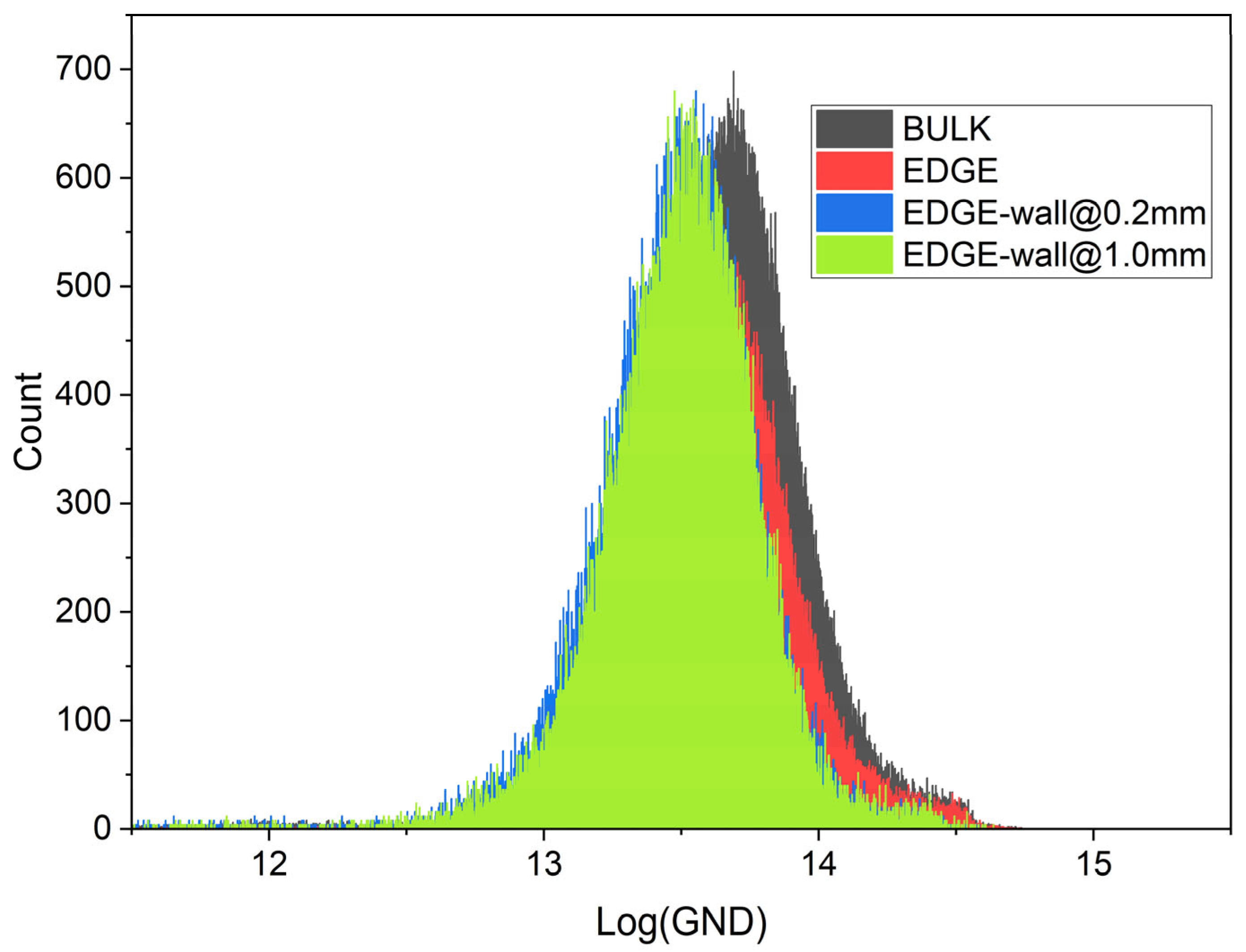
The geometrically necessary dislocation (GND) density in bulk and near-edge areas is compared in Figure 25. The distribution mode is identical but shifted toward lower GNDs near the edges of samples processed with sacrificial walls.
The primary dendrite arm spacing (PDAS) was measured in both the bulk and edge regions of the printed samples to estimate the local solidification cooling rates. According to the well-established empirical relationship between PDAS and cooling rate:
λ 1 = A × T ˙ n
where λ 1 is the PDAS in μ m , T ˙ is the cooling rate (°C/s), and A and n are material-dependent constants (typically A 50 80 and n 1 3 for Fe-based alloys) [54].
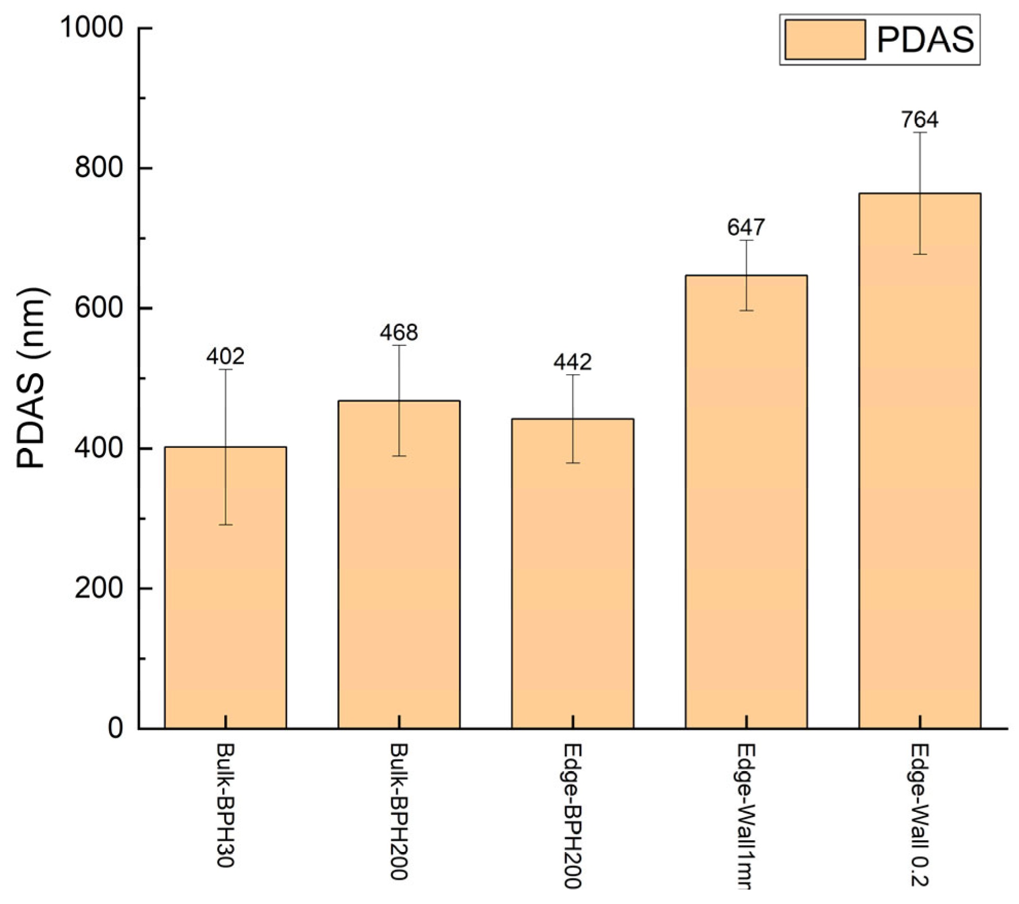
Figure 26 compares the primary dendrite arm spacing (PDAS) measured in the bulk and near-edge regions of samples produced with and without build-plate preheating, as well as those fabricated with sacrificial walls. For samples built without preheating, the average PDAS is approximately 402 nm, corresponding to a cooling rate exceeding 2 × 10⁶ °C/s. When preheating is applied, the PDAS increases to 468 nm in the bulk and 442 nm near the edge, reflecting the slightly faster solidification at the periphery. A notable coarsening of the dendritic structure occurs when thin sacrificial walls are introduced beside the coupons. The PDAS near the edges rises to 647 nm and 764 nm for walls at distances of 1 mm and 0.2 mm, respectively. The latter represents nearly a 70% increase compared to the edge PDAS of samples without walls and indicates a cooling rate roughly five times lower. The pronounced PDAS enlargement in wall-shielded samples, particularly at 0.2 mm spacing, clearly demonstrates the reduced local cooling rate near the edge, caused by elevated powder-bed temperature and limited heat dissipation. Hence, the sacrificial wall effectively functions as a thermal buffer, mitigating the temperature gradient and promoting slower solidification at the component boundaries, leading to lower residual stresses.
The stronger effect observed at a wall distance of 0.2 mm can be attributed to a modification of the local thermal boundary condition. Since the gap between the coupon and the sacrificial wall is filled with powder, heat transfer across this region occurs mainly through the effective thermal conductivity of the powder bed, including particle-contact conduction, interstitial-gas conduction, and radiative exchange, while bulk convection is expected to be limited [55]. At the smaller wall distance, repeated laser heating of the sacrificial wall increases the temperature of the surrounding powder and shortens the lateral thermal path between the wall and the coupon, thereby reducing the local cooling rate and thermal gradient. The larger PDAS measured at 0.2 mm spacing supports this interpretation. Radiation may also contribute at high temperatures, but it is not considered the dominant mechanism [55].
However, the residual stress state in LPBF is inherently anisotropic because thermal expansion and subsequent contraction of locally heated material are constrained by surrounding solid material and the platform substrate [56]. Therefore, although the present PDAS and KAM results indicate that enhanced heat extraction at the specimen perimeter is a major contributor to the observed horizontal edge cracks, a concurrent redistribution of the directional residual-stress state due to build-plate preheating cannot be excluded.
Although this approach effectively reduced the local cooling near the edges and mitigated cracking initiated from the edges, its practical implementation introduces several engineering considerations. Printing additional walls increases material consumption and building time while reducing the usable area of the building platform. The optimum wall distance from the part is expected to depend on component geometry; hence, the 0.2 mm configuration demonstrated here should be regarded as a proof of concept for localized thermal management, not an optimized industrial solution.

4. Conclusions

In this study, the processability of Fe–6.5 wt.% Si alloy by Laser Powder Bed Fusion (LPBF) was systematically investigated through compositional modification and process-level thermal management. After demonstrating the optimum process window for the alloy containing 1 wt.% Cr (Fe–6.5 wt.% Si–1 wt.% Cr), the positive effect of addition of 1 wt.% Cr via mechanical alloying was proved by enabling the establishment of a stable LPBF processing window for an alloy system that has historically exhibited poor printability. Thermodynamic analysis indicated that Cr reduces Si segregation during solidification and lowers the thermodynamic tendency for subsequent ordering, while experimental XRD phase characterization confirmed a lower fraction of ordered phases in the Cr-containing alloy. These phenomena resulted in a lower fraction of ordered phases and a corresponding reduction in solidification- and liquation-related cracking.
Build-plate preheating was shown to play a critical role in mitigating thermally induced cracking. Preheating to 200 °C successfully eliminated vertical cold cracks by reducing thermal gradients and residual stresses; however, edge-initiated horizontal cracks persisted, likely due primarily to localized heat extraction at the specimen perimeter, potentially coupled with changes in the thermomechanical constraint and residual stress distribution induced by build preheating. To address this limitation, sacrificial walls were introduced as a geometrical strategy to locally modify the cooling conditions. Microstructural analysis confirmed that the presence of sacrificial walls significantly reduced cooling rates near the edges, as evidenced by an increase in primary dendrite arm spacing. The resulting reduction in thermal stress and lattice misorientation led to a substantial decrease in crack length and crack density, which could be considered for the fabrication of mechanically sound parts after minimal machining.
Overall, the results demonstrate that a combined approach involving alloy design and localized thermal control can effectively overcome the intrinsic brittleness and cracking susceptibility of high-silicon Fe-based alloys during LPBF. Based on the former findings, adding 1 wt.% Cr does not substantially deteriorate the magnetic performance of the alloy; however, direct magnetic characterization of the LPBF-processed Fe–6.5 wt.% Si–1 wt.% Cr alloy is required to confirm this behavior. The strategies presented here provide a viable pathway for the additive manufacturing of Fe–6.5 wt.% Si components with improved structural integrity, opening new opportunities for the fabrication of complex soft magnetic components for electric motor applications.

Supplementary Materials

The following supporting information can be downloaded at: https://www.mdpi.com/article/10.3390/jmmp10090347/s1. Figure S1. EDS elemental mapping of a cross section from a Fe-6.5Si-1Cr specimen fabricated by sufficient volumetric energy density (P = 200 W, V = 1400, H = 0.05). No noticeable accumulation of Cr was detected, and the Cr distribution appears uniform throughout the microstructure; Figure S2. The processing map of LPBF-fabricated coupons made of Fe-6.5Si-1Cr alloy with hatch spacings of (a) 0.05 mm, (b) 0.10 mm, and (c) 0.13mm; Figure S3. Representative samples equipped with sacrificial walls positioned 1 mm from the coupons. Both the wall thickness and the corner radius are 1 mm.

Author Contributions

M.A.: conceptualization, methodology, writing—original draft, formal analysis, investigation. E.F.: writing—original draft, writing—review and editing, investigation. M.E.: writing—review and editing, funding acquisition, supervision. All authors have read and agreed to the published version of the manuscript.

Funding

This research was financially supported by the Natural Sciences and Engineering Research Council of Canada (NSERC) through its CREATE program led by York University.

Data Availability Statement

The raw data supporting the conclusions of this article will be made available by the authors on request.

Acknowledgments

The authors sincerely thank Zhilin Peng (Dep. of Engineering Physics, McMaster University) for providing EBSD training and facilitating access to the characterization facilities. They also gratefully acknowledge Ali Ghasemi (National University of Singapore) for valuable discussions, insightful guidance on microstructural analysis, and assistance with data analysis and visualization. Access to Thermo-Calcsoftware version 2024b was kindly provided by André Philion (Faculty of Engineering, McMaster University), whose support is also gratefully acknowledged.

Conflicts of Interest

Author Eskandar Fereiduni was employed by the company Acuren. The remaining authors declare that the research was conducted in the absence of any commercial or financial relationships that could be construed as a potential conflict of interest.

References

  1. Ouyang, G.; Chen, X.; Liang, Y.; Macziewski, C.; Cui, J. Review of Fe-6.5 wt% Si high silicon steel—A promising soft magnetic material for sub-kHz application. J. Magn. Magn. Mater. 2019, 481, 234–250. [Google Scholar] [CrossRef] [Scilit]
  2. Jiles, D. Introduction to Magnetism and Magnetic Materials, 3rd ed.; CRC Press: Boca Raton, FL, USA, 2016. [Google Scholar]
  3. McCoy, G.A.; Douglass, J.G. Premium Efficiency Motor Selection and Application Guide: A Handbook for Industry; Report No. DOE/GO-102014-4107; U.S. Department of Energy, Office of Energy Efficiency and Renewable Energy, Advanced Manufacturing Office: Washington, DC, USA, 2014.
  4. Fischer, O.; Schneider, J. Influence of deformation process on the improvement of non-oriented electrical steel. J. Magn. Magn. Mater. 2003, 254–255, 302–306. [Google Scholar] [CrossRef] [Scilit]
  5. Shimanaka, H.; Ito, Y.; Matsumura, K.; Fukuda, B. Recent development of non-oriented electrical steel sheets. J. Magn. Magn. Mater. 1982, 26, 57–64. [Google Scholar] [CrossRef] [Scilit]
  6. Constantinides, S. Energy Savings with Thin Gauge for Motors, Generators, Transformers and Inductors; Arnold Magnetic Technologies: Rochester, NY, USA, 2009. [Google Scholar]
  7. Krings, A.; Boglietti, A.; Cavagnino, A.; Sprague, S. Soft Magnetic Material Status and Trends in Electric Machines. IEEE Trans. Ind. Electron. 2017, 64, 2405–2414. [Google Scholar] [CrossRef] [Scilit]
  8. Abe, M.; Takada, Y.; Murakami, T.; Tanaka, Y.; Mihara, Y. Magnetic Properties of Commercially Produced Fe-6.5wt% Si Sheet. J. Mater. Eng. 1989, 11, 109–116. [Google Scholar] [CrossRef] [Scilit]
  9. Haiji, H.; Okada, K.; Hiratani, T.; Abe, M.; Ninomiya, M. Magnetic properties and workability of 6.5% Si steel sheet. J. Magn. Magn. Mater. 1996, 160, 109–114. [Google Scholar] [CrossRef] [Scilit]
  10. Lamichhane, T.N.; Sethuraman, L.; Dalagan, A.; Wang, H.; Keller, J.; Paranthaman, M.P. Additive manufacturing of soft magnets for electrical machines—A review. Mater. Today Phys. 2020, 15, 100255. [Google Scholar] [CrossRef] [Scilit]
  11. Ahmadnia, M.; Fereiduni, E.; Yakout, M.; Elbestawi, M.; Rm, R.K.; Vakil, G.; Muizelaar, R. Optimizing magnetic performance of Fe–50Ni alloy for electric motor cores through LPBF: A study of as-built and heat-treated scenarios. J. Mater. Res. Technol. 2024, 29, 2554–2571. [Google Scholar] [CrossRef] [Scilit]
  12. Chaudhary, V.; Sai Kiran Kumar Yadav, N.M.; Mantri, S.A.; Dasari, S.; Jagetia, A.; Ramanujan, R.V.; Banerjee, R. Additive manufacturing of functionally graded Co–Fe and Ni–Fe magnetic materials. J. Alloys Compd. 2020, 823, 153817. [Google Scholar] [CrossRef] [Scilit]
  13. Tsutsumi, Y.; Ishimoto, T.; Oishi, T.; Manaka, T.; Chen, P.; Ashida, M.; Doi, K.; Katayama, H.; Hanawa, T.; Nakano, T. Crystallographic texture- and grain boundary density-independent improvement of corrosion resistance in austenitic 316L stainless steel fabricated via laser powder bed fusion. Addit. Manuf. 2021, 45, 102066. [Google Scholar] [CrossRef] [Scilit]
  14. Ohodnicki, P. Soft Magnetic Alloys for Electrical Machine Applications: Basics, State of the Art, and R&D Opportunities; National Energy Technology Laboratory, U.S. Department of Energy: Pittsburgh, PA, USA, 2015.
  15. Shin, J.S.; Bae, J.S.; Kim, H.J.; Lee, H.M.; Lee, T.D.; Lavernia, E.J.; Lee, Z.H. Ordering–disordering phenomena and micro-hardness characteristics of B2 phase in Fe–(5–6.5%) Si alloy. Mater. Sci. Eng. A 2005, 407, 282–290. [Google Scholar] [CrossRef] [Scilit]
  16. Wang, B.; Li, G.; Wang, Y.; Su, Y.; Sun, H.; Guo, Z.; Zhang, D.; Dong, Z. Characterization of the Fe-6.5 wt% Si Strip with Rapid Cooling Coupling Deep Supercooled Solidification. ACS Omega 2021, 6, 25412–25420. [Google Scholar] [CrossRef] [Scilit]
  17. Fu, H.; Yang, Q.; Zhang, Z.; Xie, J. Effects of precipitated phase and order degree on bending properties of an Fe-6.5 wt% Si alloy with columnar grains. J. Mater. Res. 2011, 26, 1711–1718. [Google Scholar] [CrossRef] [Scilit]
  18. Li, H.; Li, Y.O.-F.; Eng Ye, F. Evolution of Microstructure and Ordering in Rolling Process of Fe-6.5 mass% Si Alloy. J. Iron Steel Res. Int. 2016, 23, 453–458. [Google Scholar] [CrossRef] [Scilit]
  19. Liang, Y.F.; Ye, F.; Lin, J.P.; Wang, Y.L.; Zhang, L.Q.; Chen, G.L. Effect of heat treatment on mechanical properties of heavily cold-rolled Fe-6.5 wt% Si alloy sheet. Sci. China Technol. Sci. 2010, 53, 1008–1011. [Google Scholar] [CrossRef] [Scilit]
  20. Wang, X.; Li, H.; Liu, Z.; Liu, H.; Wang, G.; Luo, Z.; Zhan, F.; Chen, S.; Lyu, L. Effect of cooling rate on bending behavior of 6.5 wt.% Si electrical steel thin sheets fabricated by strip casting and rolling. Mater. Charact. 2016, 111, 67–74. [Google Scholar] [CrossRef] [Scilit]
  21. Zhang, Z.; Wang, W.; Fu, H.; Xie, J. Effect of quench cooling rate on residual stress, microstructure and mechanical property of an Fe–6.5 Si alloy. Mater. Sci. Eng. A 2011, 530, 519–524. [Google Scholar] [CrossRef] [Scilit]
  22. Hwang, J.Y.; Jung, H.Y. Investigation of Cracking Behavior of Fe–6.7 Wt Pct Si Manufactured Using Laser Powder Bed Fusion. Metall. Mater. Trans. A 2023, 54, 3752–3766. [Google Scholar] [CrossRef] [Scilit]
  23. Andreiev, A.; Hoyer, K.P.; Hengsbach, F.; Haase, M.; Tasche, L.; Duschik, K.; Schaper, M. Powder bed fusion of soft-magnetic iron-based alloys with high silicon content. J. Mater. Process. Technol. 2023, 317, 117991. [Google Scholar] [CrossRef] [Scilit]
  24. Backes, C.; Mahlert, M.; Vollmer, M.; Smaga, M.; Niendorf, T.; Beck, T. Microstructure and Magnetic domain structure of assitively manufactured Fe–Si soft magnetic alloys with 3 and 9 wt.-% Si. J. Mater. Res. Technol. 2024, 29, 1691–1702. [Google Scholar] [CrossRef] [Scilit]
  25. Zanini, F.; Bonato, N.; Michieletto, D.; Alberti, L.; Carmignato, S. Laser powder bed fusion process optimization for the production of high-performance and efficient high-silicon steel electrical motor components. Prog. Addit. Manuf. 2025, 10, 6581–6592. [Google Scholar] [CrossRef] [Scilit]
  26. Cheng, Z.Y.; Liu, J.; Chen, W.S.; Sun, G.D.; Lin, X.F.; Zhu, Y.; Zhu, S.; Zhu, J.C.; Xiang, Z.D. Alloy elements added in Fe-6.5 wt% Si silicon steel and their effect on ductility and magnetic properties. Adv. Mater. Res. 2013, 750–752, 426–430. [Google Scholar] [CrossRef] [Scilit]
  27. Kim, K.N.; Pan, L.M.; Lin, J.P.; Wang, Y.L.; Lin, Z.; Chen, G.L. The effect of boron content on the processing for Fe-6.5 wt% Si electrical steel sheets. J. Magn. Magn. Mater. 2004, 277, 331–336. [Google Scholar] [CrossRef]
  28. Glezer, A.M.; Maleeva, I.V.; Zakharov, I.; Zakharov, A.I. Influence of alloy elements on the plasticity of high-silicon iron. Precis. Steels Alloys 1986, 12, 908–912. [Google Scholar] [CrossRef] [Scilit]
  29. Cheng, Z.; Liu, J.; Chen, W.; Zhu, J.; Lin, X.; Xiang, Z. Effect of 0.5 mass% Cu Addition on Ductility and Magnetic Properties of Fe-6.5Si Alloy. J. Iron Steel Res. Int. 2016, 23, 717–721. [Google Scholar] [CrossRef] [Scilit]
  30. Zhang, D.; Su, Y.; Yang, X.; Sun, H.; Guo, Z.; Wang, B.; Ma, C.; Dong, Z.; Zhu, L. Texture and Magnetic Property of Fe-6.5 wt% Si Steel Strip with Cu-Rich Particles Modification. ACS Omega 2023, 8, 8461–8472. [Google Scholar] [CrossRef] [Scilit]
  31. Yu, H.; Ming, K.; Wu, H.; Yu, Y.; Bi, X. Ordering suppression and excellent ductility in soft-magnetic Fe-6.5 wt% Si sheet by Hf addition. J. Alloys Compd. 2018, 766, 186–193. [Google Scholar] [CrossRef] [Scilit]
  32. Chen, W.; Liu, J.; Cheng, Z.; Lin, X.; Zhu, J. Effect of Chromium on Microstructure, Ordered Phase and Magnetic Properties of Fe-6.5 wt% Si Alloy. Mater. Today Proc. 2015, 2, S314–S318. [Google Scholar] [CrossRef] [Scilit]
  33. Fereiduni, E.; Ghasemi, A.; Elbestawi, M. Characterization of composite powder feedstock from powder bed fusion additive manufacturing perspective. Materials 2019, 12, 3673. [Google Scholar] [CrossRef] [Scilit]
  34. He, B.B. Two-Dimensional X-Ray Diffraction, 2nd ed.; John Wiley & Sons: Hoboken, NJ, USA, 2018. [Google Scholar]
  35. Liu, L.; Wang, D.; Deng, G.; Liu, Z.; Tan, C.; Zhou, X.; Han, C.; Jiang, R.; Yang, Y. Crack inhibition to enhance strength-ductility of CM247LC alloy fabricated by laser powder bed fusion. Mater. Sci. Eng. A 2023, 875, 145114. [Google Scholar] [CrossRef] [Scilit]
  36. Wang, G.; Huang, L.; Tan, L.; Qin, Z.; Chen, C.; Liu, F.; Zhang, Y. Effect of yttrium addition on microstructural evolution and high temperature mechanical properties of Ni-based superalloy produced by selective laser melting. Mater. Sci. Eng. A 2022, 859, 144188. [Google Scholar] [CrossRef] [Scilit]
  37. Tonelli, L.; Fortunato, A.; Ceschini, L. CoCr alloy processed by Selective Laser Melting (SLM): Effect of Laser Energy Density on microstructure, surface morphology, and hardness. J. Manuf. Process. 2020, 52, 106–119. [Google Scholar] [CrossRef] [Scilit]
  38. Wei, H.L.; Mazumder, J.; DebRoy, T. Evolution of solidification texture during additive manufacturing. Sci. Rep. 2015, 5, 16446. [Google Scholar] [CrossRef] [Scilit]
  39. Garibaldi, M.; Ashcroft, I.; Simonelli, M.; Hague, R. Metallurgy of high-silicon steel parts produced using Selective Laser Melting. Acta Mater. 2016, 110, 207–216. [Google Scholar] [CrossRef] [Scilit]
  40. Bozorth, R.M. Ferromagnetism, 1st ed.; D. Van Nostrand Company, Inc.: New York, NY, USA, 1956. [Google Scholar]
  41. Ouyang, G.; Macziewski, C.R.; Jensen, B.; Ma, T.; Choudhary, R.; Dennis, K.; Zhou, L.; Paudyal, D.; Anderson, I.; Kramer, M.J.; et al. Effects of Solidification Cooling Rates on Microstructures and Physical Properties of Fe-6.5% Si Alloys. Acta Mater. 2021, 205, 116575. [Google Scholar] [CrossRef] [Scilit]
  42. Kubaschewski, O.; Okamoto, H. Phase Diagrams of Binary Iron Alloys, 2nd ed.; ASM International: Almere, The Netherlands, 1993. [Google Scholar]
  43. Chen, S.L.; Yang, Y.; Chen, S.W.; Lu, X.G.; Chang, Y.A. Solidification simulation using scheil model in multicomponent systems. J. Phase Equilibria Diffus. 2009, 30, 429–434. [Google Scholar] [CrossRef] [Scilit]
  44. DebRoy, T.; Wei, H.L.; Zuback, J.S.; Mukherjee, T.; Elmer, J.W.; Milewski, J.O.; Beese, A.M.; Wilson-Heid, A.; De, A.; Zhang, W. Additive manufacturing of metallic components—Process, structure and properties. Prog. Mater. Sci. 2018, 92, 112–224. [Google Scholar] [CrossRef] [Scilit]
  45. Fang, P.; Xu, Y.; Li, X.; Chen, Y. Influence of Atomizing Gas and Cooling Rate on Solidification Characterization of Nickel-based Superalloy Powders. Rare Met. Mater. Eng. 2018, 47, 423–430. [Google Scholar] [CrossRef] [Scilit]
  46. Viala, B.; Degauque, J.; Fagot, M.; Baricco, M.; Ferrara, E.; Fiorillo, F. Study of the brittle behaviour of annealed Fe-6.5 wt% Si ribbons produced by planar flow casting. Mater. Sci. Eng. A 1996, 212, 62–68. [Google Scholar] [CrossRef] [Scilit]
  47. Cui, S.; Ouyang, G.; Ma, T.; Macziewski, C.R.; Levitas, V.I.; Zhou, L.; Kramer, M.J.; Cui, J. Thermodynamic and kinetic analysis of the melt spinning process of Fe-6.5 wt.% Si alloy. J. Alloys Compd. 2019, 771, 643–648. [Google Scholar] [CrossRef] [Scilit]
  48. Tang, Y.T.; Panwisawas, C.; Ghoussoub, J.N.; Gong, Y.; Clark, J.W.G.; Németh, A.A.N.; McCartney, D.G.; Reed, R.C. Alloys-by-design: Application to new superalloys for additive manufacturing. Acta Mater. 2021, 202, 417–436. [Google Scholar] [CrossRef] [Scilit]
  49. Daido, H.; Nishiuchi, M.; Pirozhkov, A.S.; Kanayat, K.; Okayama, S. Penetration and energy-loss theory of electrons in solid targets. J. Phys. D Appl. Phys. 1972, 5, 43–58. [Google Scholar] [CrossRef] [Scilit]
  50. Chakraborti, A.; Muhammad, W.; Masse, J.; Tangestani, R.; Ghasiri-Khouzani, M.; Wessman, A.; Martin, E. Role of alloy composition on micro-cracking mechanisms in additively manufactured Ni-based superalloys. Acta Mater. 2023, 255, 119089. [Google Scholar] [CrossRef] [Scilit]
  51. Bai, R.; Du, Y.; He, X.; Zhang, Y. The Influence of Cr Addition on the Microstructure and Mechanical Properties of Fe-25Mn-10Al-1.2C Lightweight Steel. Metals 2024, 14, 687. [Google Scholar] [CrossRef] [Scilit]
  52. Strantza, M.; Ganeriwala, R.K.; Clausen, B.; Phan, T.Q.; Levine, L.E.; Pagan, J.P.; Ruff, C.; King, W.E. Effect of Scanning Strategy on the formation of residual stresses in additively manufactured Ti-6Al-4V. Addit. Manuf. 2021, 45, 102003. [Google Scholar] [CrossRef] [Scilit]
  53. Polozov, I.; Kantyukov, A.; Goncharov, I.; Razumov, N.; Silin, A.; Popovich, V.; Zhu, J.N.; Popovich, A. Additive Manufacturing of Ti48Al2Cr2Nb Alloy Using Gas Atomized and Mechanically Alloyed Plasma Spheroidized Powders. Materials 2020, 13, 3952. [Google Scholar] [CrossRef] [Scilit]
  54. Bunaziv, I.; Ren, X.; Hagen, A.B.; Hovig, E.W.; Jevremovic, I.; Gulbrandsen-Dahl, S. Laser beam remelting of stainless steel plate for cladding and comparison with conventional CMT process. Int. J. Adv. Manuf. Technol. 2023, 127, 911–934. [Google Scholar] [CrossRef] [Scilit]
  55. Zhang, S.; Lane, B.; Whiting, J.; Chou, K. On thermal properties of metallic powder in laser powder bed fusion additive manufacturing. J. Manuf. Process. 2019, 47, 382–392. [Google Scholar] [CrossRef] [Scilit]
  56. Parry, L.; Ashcroft, I.A.; Wildman, R. Understanding the Effect of Laser Scan Strategy on Residual Stress in Selective Laser Melting through Thermo-Mechanical Simulation. Addit. Manuf. 2016, 12, 1–15. [Google Scholar] [CrossRef] [Scilit]
Figure 1. Schematic procedure of defect quantification of samples using ImageJ software.
Jmmp 10 00347 g001
Figure 2. Particle size distribution of (a) Fe–6.5 wt.% Si powder and (b) chromium powder. The red dashed lines correspond to cumulative volume fractions of powders (D10, D50, and D90).
Jmmp 10 00347 g002
Figure 3. Prepared feedstock of Fe–6.5 wt.% Si mixed with 1% Cr. Cr particles attached to Fe-6.5wt.% Si powders are marked with red arrows in the magnified SEM image.
Jmmp 10 00347 g003
Figure 4. (a) The processing map of LPBF-fabricated coupons made of Fe–6.5Si–1Cr alloy with a hatch spacing of 0.08 mm, (b) the top surface morphology of a sample in the lack-of-fusion region, (c) the top surface morphology of a sample processed by one of the optimum process parameter combinations, and (d) the top surface morphology of a sample in the over-fused region. All surface morphology maps are obtained with an Alicona IF microscope (Alicona Imaging GmbH, Graz, Austria).
Jmmp 10 00347 g004
Figure 5. (a) XRD analysis of the feedstock and sections parallel to the building direction of Fe–Si alloy samples fabricated at various scanning speeds (200 to 2200 mm/s), (b) low-angle range to depict B2 and D03 ordered phases.
Jmmp 10 00347 g005
Figure 6. Melt pools of samples processed by high (a) and medium volumetric energy densities (b) and their crystal orientation growth. (a) In the sample processed by (P = 300, V = 200, H = 0.1) many crystals grow horizontally or near-horizontally, perpendicular to the vertical melt pool boundary; therefore, the (100) texture would dominate on the vertical section of the sample, (b) the sample is processed with the same laser power and hatch distance but with higher scanning speed (V = 800), the crystals still grow perpendicular to the melt pool walls, situating the majority of them obliquely, hence the peak attributed to the (110) crystallographic orientation on the vertical section intensifies as depicted in Figure 5. The blue circle indicates an area of equiaxed grains resulting from a low thermal gradient; the red and green dotted lines indicate the grain boundaries and mel pool boundaries, respectively.
Jmmp 10 00347 g006
Figure 7. Phase diagram of Fe–Si alloy (adapted from [42]).
Jmmp 10 00347 g007
Figure 8. (a) Scheil–Gulliver solidification of Fe–6.5Si alloy. This model anticipates the deviation from the equilibrium (shown in dotted black line, the onset is shown by a star sign) at around 1480 °C and formation of about 0.2% B2 phase at the end of liquid-to-solid transformation. (b) Silicon concentration in A2 phase based on the Scheil model.
Jmmp 10 00347 g008
Figure 9. XRD spectra obtained from vertical sections of samples processed by laser powers of 200 W and 300 W, and from the powder sample. LPBF induces a strong texture along the building direction in favor of (100) orientation, so that the (400) crystallographic orientation is the strongest in processed samples. Comparing the peak of the ordered phase (magnified green box demonstrated on the right) shows the effect of higher laser power in amplifying the fraction of ordered phase in the microstructure.
Jmmp 10 00347 g009
Figure 10. Effect of scanning speed on the intensity of ordered phases at a laser power of 300 W and hatch spacing of 0.08 mm. The ratio of ordered to disordered peak intensity is written on the table.
Jmmp 10 00347 g010
Figure 11. As-polished micrographs of LPBF-processed Fe–Si alloy samples with (a) a hatch spacing of 0.08 mm and (b) a laser power of 200 W at various hatch distances and scanning speeds. The direction of laser scanning is perpendicular to and across the section, alternately.
Jmmp 10 00347 g011
Figure 12. (a) Microstructure of a sample processed by P = 200 W, V = 600 mm/s, H = 0.13 mm. Due to the large hatch spacing, lack of fusion is frequently seen between melt tracks. (b) A solidification crack. Green lines indicate the melt pool boundaries and the red dashed lines delineate the grain boundaries. Blue lines represent the cellular/dendritic solidification directionality and a crack initiated from a pore due to stress concentration.
Jmmp 10 00347 g012
Figure 13. Three types of cracks observed within fabricated Fe–Si alloy samples. (a) Solidification crack and its dendritic features; (b) transgranular solid-state cracks propagated through several melt pools or grains; and (c) liquation cracking beneath melt pool boundaries. The green dotted lines represent melt pool boundaries, while the red arrows in (b) indicate microstructure separation caused by transgranular crack.
Jmmp 10 00347 g013
Figure 14. Optical and SEM micrographs of the sample (P200_V800_H0.08), (a) Optical image of vertical section near the top surface showing the epitaxial long grains, (b) an intergranular liquation crack shown with yellow arrow on grain boundaries, (c) SEM-SE image of the surface showing the solidification cracks (yellow arrow) and the large cold intragranular crack, the yellow star indicates partitioning of a grain, and (d) EDS analysis on an area near the onset of the crack to demonstrate the distribution of silicon. Grain and melt-pool boundaries are represented by red and green dashed lines, respectively.
Jmmp 10 00347 g014
Figure 15. (a) Horizontal cracks observed on a sample processed by (P = 300 W, V = 1000 mm/s, and H = 0.08 mm) and (b) residual stress measured on a side of samples with equal scanning speed and hatch spacing but different laser powers.
Jmmp 10 00347 g015
Figure 16. Crack area fraction (CAF), porosity area fraction (PAF), and cumulative crack length (CCL) of samples processed by a laser power of 200 W at different hatch distances and scanning speeds.
Jmmp 10 00347 g016
Figure 17. (a) Scheil–Gulliver solidification route of the Fe–6.5Si and Fe–6.5Si–1Cr alloys. The alloy containing Cr (black dashed arrow) starts to form the B2-ordered phase later than the one without Cr (blue dashed arrow). (b) Silicon concentration in the liquid during solidification. By approaching the end of the solidification process, the concentration of Si in the remaining liquid increases exponentially in both alloys; however, the concentration of Si in the Cr-containing alloy (black curve) stays lower than that in the Fe–6.5Si alloy (green curve) throughout the process.
Jmmp 10 00347 g017
Figure 18. Contour line of driving force (J/mol) to form B2-ordered phase in temperatures below the solidus line. As evident, increasing the Cr concentration in the alloy composition lowers the driving force and hence plays in favor of A2 disordered phase.
Jmmp 10 00347 g018
Figure 19. XRD spectra of samples made of Fe–6.5 wt.% Si with and without added chromium. The calculated ratio of ordered to disordered peak is included in the picture.
Jmmp 10 00347 g019
Figure 20. Large optical micrograph of sample made of Fe–6.5 wt.% Si alloy (a) and Fe–6.5 wt.% Si–1 wt.% Cr (b); both micrographs are obtained from similar build height of coupons processed with identical process variable combination (P200-V800-H0.08), (c,d) SEM image of a typical solidification crack present on the sample shown in (a).
Jmmp 10 00347 g020
Figure 21. ECC values in samples made of the alloy with and without chromium.
Jmmp 10 00347 g021
Figure 22. EBSD results for samples processed by laser power = 200 W, scanning speed = 800 mm/s, and hatch distance = 0.08 mm. (af) made of Fe–6.5 wt.% Si without build preheat, (gl) made of Fe–6.5 wt.% Si–1 wt.% Cr without build preheat, and (mr) made of Fe–6.5 wt.% Si–1 wt.% Cr with BPH = 200 °C. IPF maps parallel to the building direction (IPF-Z) (a,g,m), IPF maps normal to the section (IPF-X) (b,h,n), texture plot of the section toward the building direction (c,i,o) and perpendicular to the section (d,j,p), area-weighted grain size distribution with calculated mean grain size (e,k,q), and KAM of lattice (f,l,r).
Jmmp 10 00347 g022
Figure 23. Vertical section micrographs of samples made of Fe–6.5 wt.% Si–1 wt.% Cr processed by laser power, scanning speed, and hatch distance of 200, 800, and 0.08 mm, respectively, with (a) BPH = 30 °C and (b) BPH = 200 °C.
Jmmp 10 00347 g023
Figure 24. Kernel Average Misorientation (KAM) maps of the sample printed without a sacrificial wall: (a) bulk region and (b) area near the edge; and KAM maps of the edge regions of samples equipped with sacrificial walls positioned at (c) 1 mm and (d) 0.2 mm from the coupon perimeter.
Jmmp 10 00347 g024
Figure 25. Geometrically necessary dislocation density distribution in the bulk area and near the edge of samples processed with and without sacrificial walls.
Jmmp 10 00347 g025
Figure 26. Primary dendrite arm spacing in the bulk and near-edge areas of samples processed with and without build preheating, as well as samples printed encircled by sacrificial walls.
Jmmp 10 00347 g026
Table 1. Nominal chemical composition of the Fe–Si powder, as declared by the supplier.
PowderElements (wt.%)
Fe–6.5 wt.% SiFeSiCrMnCoCuMoP
Bal.6.3–6.70.070.060.030.040.010.01
Table 2. Process variables utilized to fabricate samples.
Laser power (P) (W)100, 200, 300
Scanning speed (V) (mm/s)200, 400, 600, 800, 1000, 1200, 1400, 1800, 2200, 2600, 3000
Hatch spacing (H) (mm)0.05, 0.08, 0.10, 0.13
Scanning vector length (VL)100, 5, 2
Build preheating temperature (°C)30, 200
Layer thickness (mm)0.04
Hatch rotation90°, 67°
Disclaimer/Publisher’s Note: The statements, opinions and data contained in all publications are solely those of the individual author(s) and contributor(s) and not of MDPI and/or the editor(s). MDPI and/or the editor(s) disclaim responsibility for any injury to people or property resulting from any ideas, methods, instructions or products referred to in the content.