Proceeding Paper

Influence of Residual Stresses of Sputtered Thin Film Electrodes for Dielectric Elastomer Applications †

1
Department of Sensors and Thin Films, University of Applied Sciences of Saarland, Goebenstraße 40, 66117 Saarbrücken, Germany
2
Department of System Engineering, Department of Materials Science and Engineering, Saarland University, 66123 Saarbruecken, Germany
*
Author to whom correspondence should be addressed.
Presented at the First International Electronic Conference on Actuator Technology: Materials, Devices and Applications, 23–27 November 2020; Available online: https://iecat2020.sciforum.net/.
Proceedings 2020, 64(1), 2; https://doi.org/10.3390/IeCAT2020-08492
Published: 20 November 2020

Abstract

:
This paper focuses on the electromechanical properties of novel sub-micron compliant metallic thin film electrodes for dielectric elastomer membranes. Electrodes with thicknesses within the range of 10–20 nm and different residual stress states are explored. Both pure nickel films and sandwiches of nickel (Ni) and carbon (C) are deposited by direct current (DC) magnetron sputtering onto pre-stretched silicone elastomer membranes. Both 37.5% biaxial pre-stretch and 57.5% uniaxial pre-stretch under pure shear condition (PSC) are considered in the conducted investigation. After the coating process is completed, the elastomer is allowed to relax. In the contracted configuration, it exhibits a wrinkled surface. After this state is reached, the electromechanical characterization is performed. All types of films reveal a low initial resistance (around 100 Ω/square). Depending on the kind of pre-stretch and the electrode material, a strain of 100% without any major degradation is achieved. It is also shown how the residual stress of the layers can be influenced by suitable sputtering parameters. As a result, low residual film stress significantly improves the electromechanical properties of PSC pre-stretched elastomers, but have only a minor influence on the biaxially pre-stretched ones, regarding the Ni and the Ni + C thin films. This phenomenon is directly connected to the failure mechanisms observed on the two types of pre-stretched membranes. With reversed layer order, i.e., C + Ni electrodes, the residual stress state of Ni does not influence the electromechanical properties for both the biaxially pre-stretched and the PSC pre-stretched coated membranes. The results are of fundamental importance for understanding the role of residual stresses for the creation of electromechanically stable and highly conductive electrode films, to be used in dielectric elastomer (DE) applications.

1. Introduction

Dielectric elastomer (DE) transducers represent a unique class of sensors and actuators that combine many interesting features, such as large deformation, lightweight, silent operations, scalability, and energy efficiency, amongst others [1,2].
A DE can be interpreted as a flexible capacitor consisting of a flexible polymeric membrane sandwiched by two compliant electrodes [3]. The application of a few kilovolts results in an attraction of the electrodes, accompanied by a simultaneous in-plane expansion of the polymeric membrane. The electro-mechanical compressive stress induced on the membrane is described by the Maxwell stress σMax, given as follows:
σ M a x = ε r ε 0 ( V d ) 2 ,
with the relative permittivity εr, vacuum dielectric constant ε0, voltage V, and distance between the electrodes d [4].
The electrodes are of crucial importance regarding the functionality of the DE. They have to be soft and highly conductive even at high strain levels up to 100%. Furthermore, patternability and stretchability are required [5]. Usually, carbon black electrodes, i.e., a mixture of carbon and silicone, with a thickness of several µm, are used to obtain soft and stretchable electrodes. Such types of electrodes, however, exhibit a relatively high initial resistance of around 50 kΩ per square [6]. Metallic thin film electrodes with a thickness in the nm-range provide better conductivity in the order of 100 Ω per square, however they stiffen the system and have only limited elasticity. Scientists tried to overcome these drawbacks by creating corrugated [7] or wrinkled surfaces [8], by generating stretchable zig-zag [9], meander [10], or kirigami structures [11], or by applying sophisticated manufacturing methods such as ion implantation [12].
This study focuses on sputtered wrinkled metallic electrodes, a well-known principle in the field of flexible electronics [13,14]. In here, an either biaxially or under pure-shear condition uniaxially (PSC) pre-stretched silicone membrane is sputter coated with either a pure nickel thin film or a sandwich consisting of nickel and carbon with a thickness of 10 nm or 20 nm respectively. After the deposition process, the membrane is allowed to relax whereby a wrinkled metallic electrode is obtained. These wrinkles act as a mechanical buffer when a strain is applied during actuation. Electromechanical tensile tests are performed to characterize the thin film electrodes. The influence of the residual stress state of the respective thin film electrode on the electromechanical properties of the DE is also clarified. The material selection of nickel and carbon is motivated by our own previous research on compliant electrodes [15] and sensor thin films [16,17].

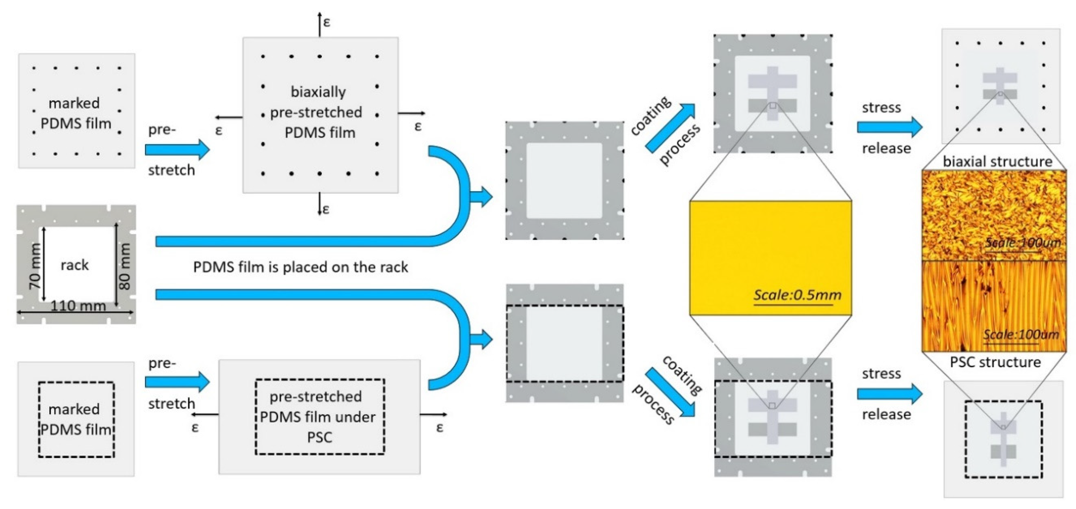
2. Materials and Methods

In this work, Wacker Elastosil 2030 with a thickness of 47.5 µm ± 5% was used as a silicone membrane (PDMS membrane). The membrane was sputter-coated in a pre-stretched state. Either a 37.5% biaxial pre-stretch or a 57.5% uniaxial pre-stretch under pure-shear conditions (PSC) were considered in this paper. As soon as the pre-stretch was applied, the silicone film was placed on a metal rack, dedusted with deionized air, and then coated in the vacuum chamber. A mirror-like surface was obtained after the sputtering. By carefully removing the silicone from the rack after the coating, the membrane was allowed to relax. It shrunk to its initial dimension, thus forcing the metallic thin film to form wrinkles. Depending on the type of pre-stretch, an aligned wrinkle structure (PSC pre-stretch) or a random wrinkle orientation (biaxial pre-stretch) was obtained (cf. Figure 1).
The coating was performed in a 45 × 45 × 45 cm3 vacuum chamber from the company CCR. The chamber was equipped with a turbo molecular pump, a downstream throttle valve (VAT), and two heads for magnetron targets with a diameter of 127 mm. One head carried a nickel target, while the other one, a carbon target. The samples were placed with a sample to target a distance of 45 mm on a movable carrier. The chamber had no load lock, hence it was vented with nitrogen after every process. Once the vacuum chamber was evacuated to a background pressure less than 1 × 10⁻⁵ mbar, three purge-pump cycles with argon to a pressure of 1 × 10⁻¹ mbar were executed, to ensure clean sputtering conditions. Then, argon (purity 99.999%) was let into the vacuum chamber with a constant flow of 15 sccm. The process pressure was controlled in the range between 1.5 µbar and 36 µbar, thanks to the appropriate setting of the throttle valve. When the process pressure was adjusted, the first target was pre-sputtered for 1.5 min with 300 W DC power. Then, the sample was transferred under the target for the coating process. After a certain process time, the sample was removed again. If a sandwich layer was desired, the procedure would be subsequently executed in the same manner at the second target.
The thin films were deposited on both surfaces of the PDMS, by applying cross-shaped shadow masks rotated against each other by 180 degrees (see Figure 2). The long cross bar (10 mm × 50 mm) represented the active area to be examined, while the perpendicular bars served as electrical contacts. Three types of electrodes were researched in this study. Pure nickel thin films with a thickness of 10 nm or a bi-layer sandwich, with an overall thickness of 20 nm, consisting of carbon (10 nm) and Ni (10 nm), were manufactured. Both electrode layer sequences, Ni + C as well as C + Ni, were investigated in this study. Due to different deposition rates of nickel and carbon, the 10 nm thick Ni-layer corresponded to a sputter time of 5 s, whereas 60 s was needed to achieve a 10 nm thick carbon layer. Further details on the manufacturing process are given in [15].
The residual stress state of the deposited thin films was examined on glass slides. Glass slides were sputter-coated, and the curvature of the slides was measured before and after the coating process. The residual stress of the deposited thin film could then be calculated with the aid of the Stoney equation [18,19]:
σ R = E s 6 ( 1 v s ) h s 2 h f ( 1 R 1 R 0 ) ,
with the Young’s Modulus of the substrate Es, the Poisson ratio of the substrate vs, the thickness of the substrate hs, the thickness of the film hf, the initial radius of the glass slide R0, and the radius of the glass slide after the sputter coating R.
The radius of the glass slides was determined by means of a white light profilometer Microprof from the company FRT. The surface profile of the slides was measured with a line scan. Then, the software fitted a section of a circle to the 2D profile and calculated the corresponding radius of curvature. Overall, nickel layers produced at 13 different process pressures in the range between 1.5 µbar and 36 µbar were investigated. The sputter time of 45 s, the power of 300 W DC, and the sample to target distance of 45 mm were kept constant for this series of experiments. For each pressure level, the residual stress was calculated and plotted as a function of the process pressure. A fit of the measured data was then performed with OriginLab.
A direct thickness measurement of the thin film electrode on the soft and transparent PDMS is not possible. Hence, the thickness of the layers was determined by means of the deposition rate of the respective target materials. A sputter-deposited thin film of either carbon or nickel was created on glass slides, with a small cover glass in the center to produce a step with the thickness of the film. The deposited thin film was produced with the same sputter conditions as those used for manufacturing the DE membranes. Then, this step was measured ascending and descending with a Dektak 150 tactile profilometer. The deposition rate was calculated from the step height and the corresponding sputter time. The associated linear fit was done by OriginLab. For carbon, a series of coatings with sputter times between 0 and 5 min were performed at a process pressure of 1.5 µbar. For nickel, sputter times between 0 and 2 min were chosen with pressures of 1.5 µbar and 18 µbar, respectively.
Both PSC and biaxially pre-stretched membranes, coated on only one side with either Ni, Ni + C, or C + Ni thin film electrodes, were tested on a uniaxial tensile tester. For each type of electrode, both electrodes with nickel thin films deposited at high and low process pressure were manufactured and examined. The schematic test arrangement is shown in Figure 2 (for a detailed description of the tensile tester, the author may refer to [20]). With the tensile direction being perpendicular to the long side, and a length to width ratio of the active area equal to 5:1, the uniaxial tensile test could be interpreted as a pure shear tensile test [21]. The transverse contraction was negligible. During the tests, an LCR meter (Hameg MH8118) was used to measure the resistance versus the applied strain. Starting at 0% strain, the strain level was increased stepwise with a complete strain release between the steps. Every strain level was kept constant for 25 s, and the electrical resistance was recorded and averaged over time. The averaged resistance was then plotted as a function of the corresponding strain. An increment of 10% was chosen up to an absolute strain of 30%, followed by an increase of 5% up to the electrical failure (defined to be 100 kΩ in this study). Two smaller steps of 2.5% strain increments were also included around the level of pre-stretch.

3. Results and Discussion

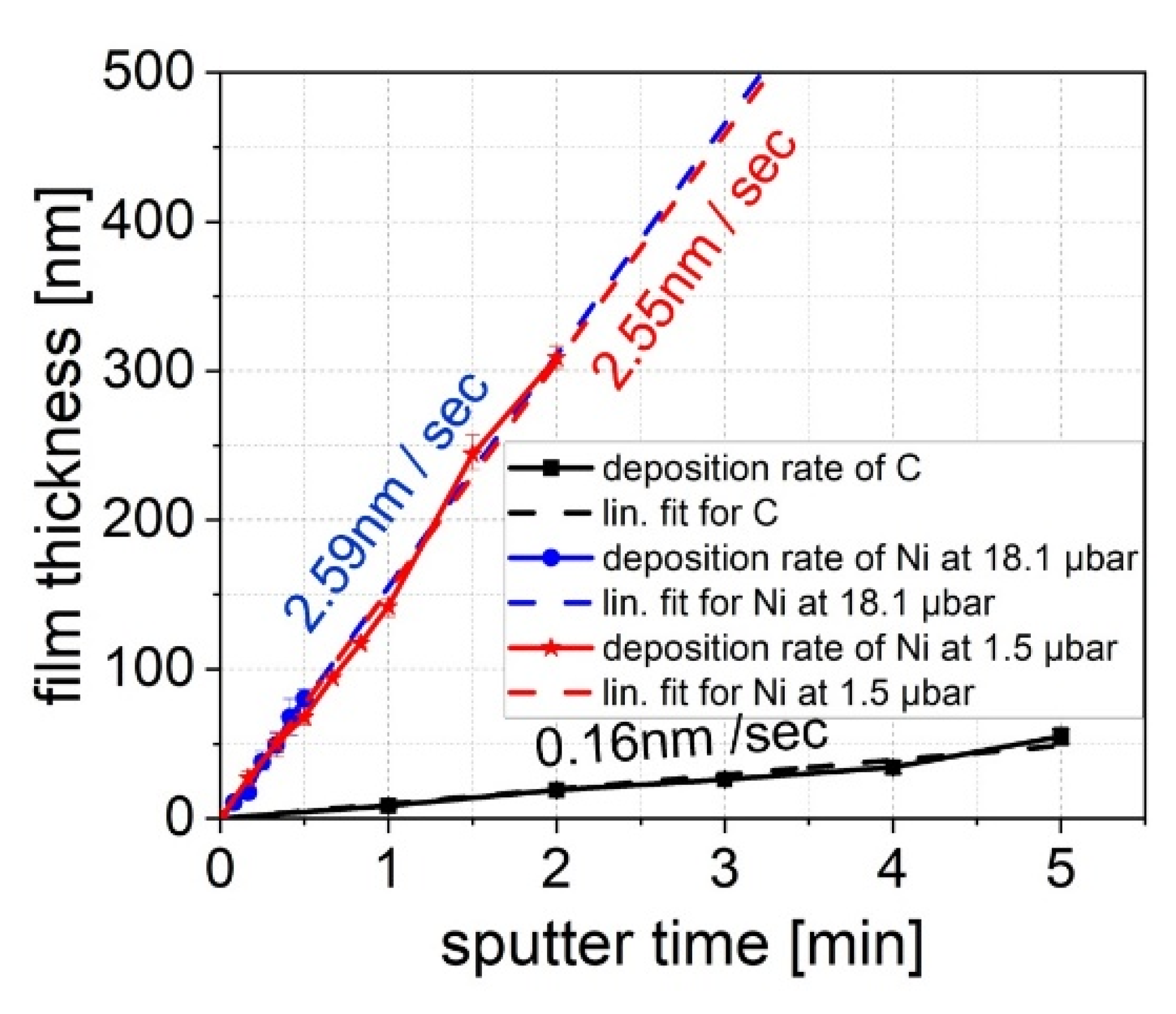
3.1. Deposition Rate

The result of the deposition rate analysis is shown in Figure 3. The deposition rate of carbon is 0.16 nm per second, so 10 nm of a thin carbon film is produced in about one minute. Nickel layers sputtered at two very different process pressures (1.5 µbar and 18.1 µbar) have comparable deposition rates of 2.55 nm/s and of 2.59 nm/s, respectively. In both cases, although they differ greatly in their residual stresses (see below), the actual thickness of nickel thin films produced in five seconds is slightly lower than the theoretical thickness calculated by the deposition rate. This is related to the process control during the manufacturing (for further details see [15]). In general, the deposition rate is dependent on several parameters such as the process pressure, the target to substrate distance, the vacuum chamber, and the deposition power, amongst others [22,23,24]. It increases first with a higher process pressure, due to a rise in the number of ions [24]. With a further increase of the process pressure, the probability of an expelled atom to reach the substrate decreases due to interatomic collisions and back diffusion [22,24]. These two competing processes could be responsible for the obtained results, i.e., the deposition rate for both Ni-processes are hardly distinguishable.

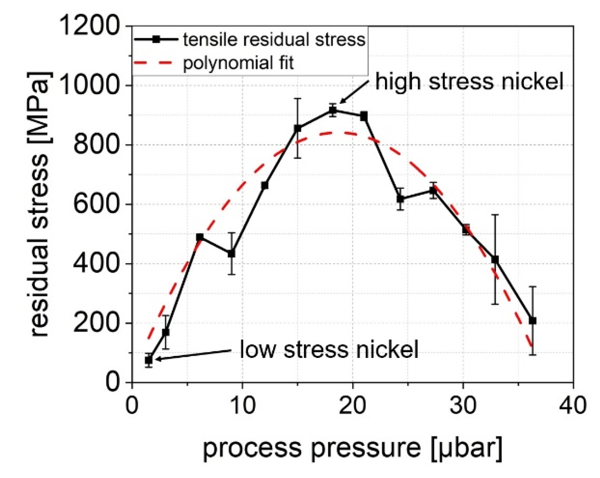
3.2. Residual Stress Analysis

In Figure 4, the measured data of the residual stress analysis and the corresponding fit is plotted as a function of the process pressure. All measured stresses are tensile residual stresses. The curve is shaped similarly to a concave parabola, which starts with a local minimum of 75 MPa at around 1.5 µbar, followed by an increase of the residual stress up to 917 MPa at 18 µbar. Then, the residual stress drops again to 208 MPa at 36 µbar. These results are based on Equation 2 with Young’s modulus (of glass) of 64 GPa [25], a Poisson ratio of 0.2 [25], a thickness of the glass slides of 0.5 mm, and a film thickness of 115 nm. The difference of film thickness between a Ni (low stress) and a Ni (high stress) layer due to the different deposition rate is 2 nm. For the interpretation of the residual stress state of the examined thin films, this thickness deviation is negligible.
Ni (high stress) layers have good adhesion on glass slides, as shown in previous tests. Hence, for the examination of the series of nickel electrodes, 18.1 µbar was first chosen as process pressure. It could be observed, however, that the Ni (high stress) layers tend to form cracks when deposited onto PSC pre-stretched membranes. By depositing Ni (low stress) electrodes, sputtered at 1.5 µbar on silicon membranes, the crack formation can be avoided completely. However, the nickel thin film manufactured at 36.3 µbar is still prone to crack formation on silicone. Based on this observation, the residual stress study focuses on the Ni (low-stress) films deposited at low process pressures.
Regarding the wrinkle formation after the relaxation of the electrodes with low-stress nickel and high-stress nickel, no significant optical differences can be observed.

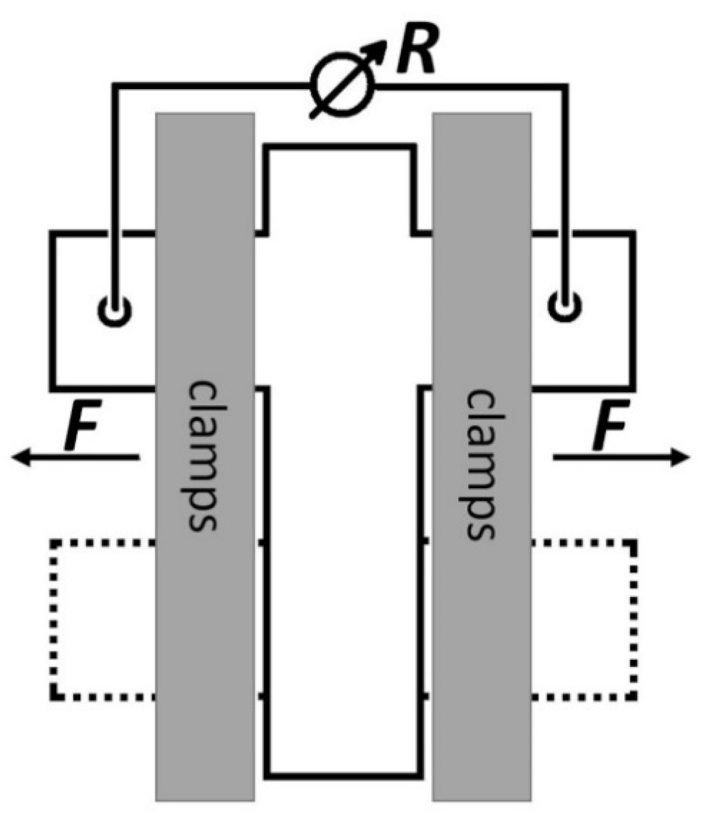
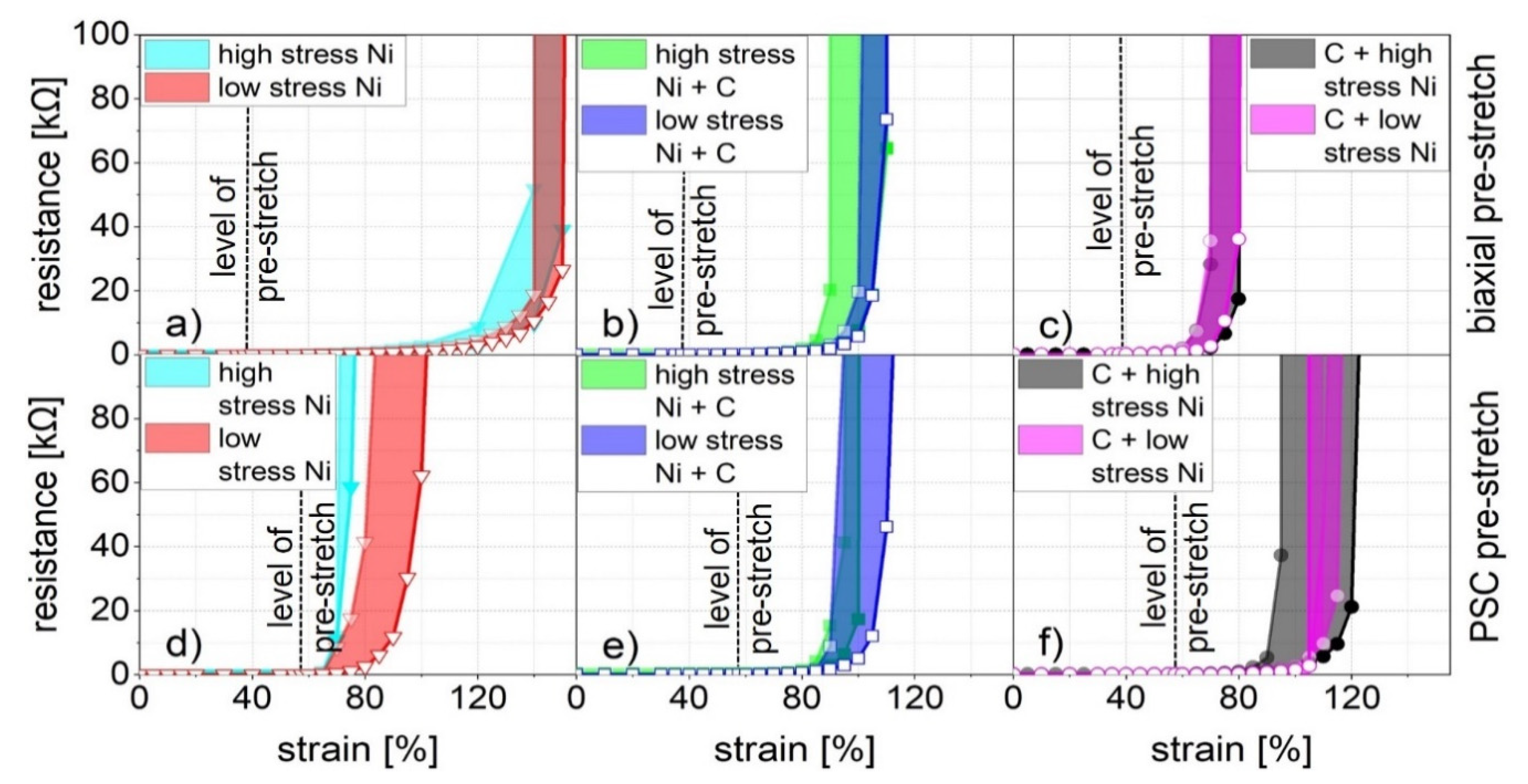
3.3. Resistance vs. Strain Measurements

The resistance versus strain for Ni, Ni + C, and C + Ni thin film electrodes, deposited on either biaxially pre-stretched or PSC-pre-stretched membranes, is illustrated in Figure 5. In the first row (Figure 5a–c), the results of the biaxially pre-stretched silicone membrane are shown, whereas PSC pre-stretched silicone is represented in the second line (Figure 5d–f). Each column depicts the results of one type of thin film, starting from pure nickel (Figure 5a,d), followed by Ni + C (b and e), and then C+Ni (c and f), when moving from left to right. Each graph contains two colored areas, representing the data family of at least three specimens of the corresponding thin film type. The maximum and the minimum values of the series of the examined type of electrode frames the colored area.
Overall, there are some characteristics that are independent of the residual stress state. For all layer combinations, the threshold of the resistance increase is located at strain levels above the respective level of pre-stretch (LoP). For the biaxially pre-stretched membranes, this threshold is shifted to higher strain levels with respect to the corresponding LoP. Furthermore, the resistance increase on biaxially pre-stretched membranes is more gradual, while electrodes deposited on PSC membranes show a fast and steep increase of the resistance above the LoP. This phenomenon is related to the difference in the failure mechanisms of the two types of pre-stretch. If a low resistance is needed at high strain levels, a pure Ni thin film can be used on biaxially pre-stretched membranes, whereas on PSC membranes the C + Ni electrodes give the best results. These results obtained here for Ni layers correspond to the trends of the previous NiCr study [15].
From the results, it can be concluded that both the different thin film configuration and the type of pre-stretch are influenced in different ways by the residual stress state of the electrodes. Ni and Ni + C reveal the same characteristics. On foils with a biaxial pre-stretch, the residual stress state of the electrode does not influence the resistance curve at high strain levels. The width of the colored region is narrowed for the low residual stress specimen. The maximum curves of both the low and the high residual stress layer are congruent, though. When a low-stress layer is manufactured onto membranes pre-stretched under PSC conditions, the threshold of the resistance increase can be shifted towards higher strain levels.
The different failure mechanism of the biaxially and PSC pre-stretched membranes is responsible for the different results. When the biaxially pre-stretched membrane is allowed to relax after the coating, a wrinkled surface with a random wrinkle orientation is obtained. A PSC membrane exhibits aligned wrinkles after relaxation. During the strain tests, this aligned structure is unfolded and flattened. When the LoP is reached, a perfectly flat electrode surface is obtained in theory. By exceeding the LoP cracks in the metallic electrode can be created, which can easily propagate through the flat surface. Hence, few but large cracks are responsible for the drastic resistance increase. In this case, the intrinsic residual stress of the electrode directly influences the driving force for the crack formation. A high residual tensile stress promotes crack formation and propagation. With low residual stress, on the other hand, crack formation is delayed and the threshold is shifted to higher levels of strain. A biaxially pre-stretched membrane is only partially flattened during a uniaxial tensile test. Even at strain levels above the LoP, wrinkles parallel to the strain direction are still present. The remaining wrinkled structure leads, during a tensile test, to an inhomogeneous stress distribution over the surface. Once a crack is created, it is not able to propagate through the whole electrode in one step, since it stops when it crosses wrinkles oriented perpendicularly to the crack growth direction. Hence, a huge number of small cracks are present. In general, this is advantageous when a low resistance at high strain is desired [26]. This phenomenon of intrinsic impediments of crack propagation was shown before on coated surfaces with different roughnesses [27]. The results of the mentioned study could easily be assigned to a randomly wrinkled surface. For biaxially pre-stretched membranes, the failure mechanism dominates over the residual stress state.
A Ni + C electrode consisting of a nickel layer with low stresses on PSC pre-stretched silicone exhibits degradation at strain levels 10% higher, compared to the Ni + C electrode with high residual stresses (see Figure 5d). Regarding the pure nickel electrodes on membranes with a PSC pre-stretch, replacing the high-stress nickel with a low-stress nickel thin film provides an enhancement of almost 30% (compare Figure 5e). In our study, only the residual stress of the Ni layer is investigated. The properties of the carbon layers are the same for all measured sandwich electrodes. The performance of the Ni + C electrode is determined by the interaction of both thin film layers, and not only by the nickel thin film. Therefore, the change in the properties of the sandwich Ni + C layer is not as obvious as the drastic change of a pure nickel electrode.
If Ni is deposited as a top layer on a carbon layer, i.e., a C + Ni sandwich (Figure 5c,f), then the residual stress of the nickel layer does not influence the resistance at high strain levels. The carbon bottom-layer somehow absorbs the high residual stress of the nickel layer. In that case, a reduction of the residual stress of the nickel top layer does not lead to any further improvement, but also to no degradation of the electromechanical properties. The exact mechanism of how carbon works has not been clarified yet and will be part of the investigation for future research.

4. Conclusions

Based on the conducted study, it can be concluded that the reduction of residual stresses of a thin film electrode can improve, under certain circumstances, the electromechanical properties of a DE membrane. For biaxially pre-stretched membranes tested under pure shear conditions, the resistance increase is solely dominated by the failure mechanism of the randomly oriented wrinkles, and not by the residual stress state of the compliant electrode. Regarding the electromechanical properties, neither benefits nor drawbacks are observed in the case of low-stress nickel layers. The same is true for sandwich layers if Ni is the top-layer. In that case, the carbon bottom layer absorbs the residual stresses of the top-layer. For membranes, both pre-stretched and tested under pure shear conditions, the residual stress reduction of the nickel layers results in a shift of the resistance increase towards higher strain levels. The strain threshold is thus enhanced by almost 30% for pure nickel electrodes. Thus, electrodes with low residual stress states offer the chance of improving the electromechanical properties. Furthermore, the process parameters which are applied to obtain films with low stresses, avoid crack formation during sputtering. Hence, it is highly recommended to use thin films with low residual stresses for all kind of DE applications.

Author Contributions

Conceptualization, J.H., S.C., J.N.; methodology, J.H., S.C., J.N.; validation, J.H., S.C., J.N., G.S.; investigation, J.H.; resources, G.S., G.R., S.S.; data curation, J.H.; writing—original draft preparation, J.H.; writing—review and editing, G.S., G.R.; visualization, J.H.; supervision, G.S., G.R., S.S.; project administration, G.S., G.R., S.S.; funding acquisition, G.S., G.R., S.S. All authors have read and agreed to the published version of the manuscript.

Funding

This research was generously funded by DFG, German Research Foundation, grant number SCHU 1609/7-1.

Acknowledgments

The authors gratefully acknowledge the support of the Deutsche Forschungsgemeinschaft (DFG, German Research Foundation) through Priority Program SPP 2206 “Cooperative Multistage Multistable Microactuator Systems” (Projects: RI3030/2-1, SCHU1609/7-1, SE704/9-1). We also gratefully acknowledge the support of the whole Sensors and Thin Film Group, especially the support of our student assistant Simon Kraß.

Conflicts of Interest

The authors declare no conflict of interest.

References

  1. Rosset, S.; Shea, H.R. Flexible and stretchable electrodes for dielectric elastomer actuators. Appl. Phys. A 2013, 110, 281–307. [Google Scholar] [CrossRef]
  2. Romasanta, L.J.; Lopez-Manchado, M.A.; Verdejo, R. Increasing the performance of dielectric elastomer actuators: A review from the materials perspective. Prog. Polym. Sci. 2015, 51, 188–211. [Google Scholar] [CrossRef]
  3. Hau, S.; Rizzello, G.; Seelecke, S. A novel dielectric elastomer membrane actuator concept for high-force applications. Extrem. Mech. Lett. 2018, 23, 24–28. [Google Scholar] [CrossRef]
  4. Linnebach, P.; Simone, F.; Rizzello, G.; Seelecke, S. Development, manufacturing, and validation of a dielectric elastomer membrane actuator–driven contactor. J. Intell. Mater. Syst. Struct. 2019, 30, 636–648. [Google Scholar] [CrossRef]
  5. Pelrine, R.E.; Kornbluh, R.D.; Joseph, J.P. Electrostriction of polymer dielectrics with compliant electrodes as a means of actuation. Sens. Actuators A Phys. 1998, 64, 77–85. [Google Scholar] [CrossRef]
  6. Fasolt, B.; Hodgins, M.; Rizzello, G.; Seelecke, S. Effect of screen printing parameters on sensor and actuator performance of dielectric elastomer (DE) membranes. Sens. Actuators A Phys. 2017, 265, 10–19. [Google Scholar] [CrossRef]
  7. Benslimane, M.; Kiil, H.-E.; Tryson, M.J. Electromechanical properties of novel large strain PolyPower film and laminate components for DEAP actuator and sensor applications. In Proceedings of the Electroactive Polymer Actuators and Devices (EAPAD 2010), San Diego, CA, USA, 7–11 March 2010; p. 764231. [Google Scholar]
  8. Lacour, S.P.; Wagner, S.; Huang, Z.; Suo, Z. Stretchable gold conductors on elastomeric substrates. Appl. Phys. Lett. 2003, 82, 2404–2406. [Google Scholar] [CrossRef]
  9. Pelrine, R.; Kornbluh, R.; Joseph, J.; Heydt, R.; Pei, Q.; Chiba, S. High-field deformation of elastomeric dielectrics for actuators. Mater. Sci. Eng. C 2000, 11, 89–100. [Google Scholar] [CrossRef]
  10. Verplancke, R.; Bossuyt, F.; Cuypers, D.; Vanfleteren, J. Thin Film stretchable electronics technology based on meandering interconnections: Fabrication and mechanical performance. J. Micromech. Microeng. 2012, 22, 15002. [Google Scholar] [CrossRef]
  11. Huang, S.; Liu, Y.; Zhao, Y.; Ren, Z.; Guo, C.F. Flexible Electronics: Stretchable Electrodes and Their Future. Adv. Funct. Mater. 2019, 29, 1805924. [Google Scholar] [CrossRef]
  12. Akbari, S.; Shea, H. Arrays of 100μm x 100μm dielectric elastomer actuators to strain the single cells. Procedia Eng. 2011, 25, 693–696. [Google Scholar] [CrossRef]
  13. Cheng, T.; Zhang, Y.; Lai, W.-Y.; Huang, W. Stretchable Thin Film Electrodes for Flexible Electronics with High Deformability and Stretchability. Adv. Mater. Weinheim. 2015, 27, 3349–3376. [Google Scholar] [CrossRef] [PubMed]
  14. Kaltenbrunner, M.; Sekitani, T.; Reeder, J.; Yokota, T.; Kuribara, K.; Tokuhara, T.; Drack, M.; Schwödiauer, R.; Graz, I.; Bauer-Gogonea, S.; et al. An ultra-lightweight design for imperceptible plastic electronics. Nature 2013, 499, 458–463. [Google Scholar] [CrossRef] [PubMed]
  15. Hubertus, J.; Fasolt, B.; Linnebach, P.; Seelecke, S.; Schultes, G. Electromechanical evaluation of sub-micron NiCr-carbon thin films as highly conductive and compliant electrodes for dielectric elastomers. Sens. Actuators A Phys. 2020, 315, 112243. [Google Scholar] [CrossRef]
  16. Schultes, G.; Schmid-Engel, H.; Schwebke, S.; Werner, U. Granular metal–carbon nanocomposites as piezoresistive sensor films—Part 1: Experimental results and morphology. J. Sens. Sens. Syst. 2018, 7, 1–11. [Google Scholar] [CrossRef]
  17. Koppert, R.; Uhlig, S.; Schmid-Engel, H.; Göttel, D.; Probst, A.-C.; Schultes, G.; Werner, U. Structural and physical properties of highly piezoresistive nickel containing hydrogenated carbon thin films. Diam. Relat. Mater. 2012, 25, 50–58. [Google Scholar] [CrossRef]
  18. Ardigo, M.R.; Ahmed, M.; Besnard, A. Stoney Formula: Investigation of Curvature Measurements by Optical Profilometer. AMR 2014, 996, 361–366. [Google Scholar] [CrossRef]
  19. Stoney, G.G. The tension of metallic films deposited by electrolysis. Proc. R. Soc. Lond. A 1909, 82, 172–175. [Google Scholar] [CrossRef]
  20. Hodgins, M.; York, A.; Seelecke, S. Systematic experimental characterization of dielectric elastomer membranes using a custom-built tensile test rig. J. Intell. Mater. Syst. Struct. 2017, 28, 2117–2128. [Google Scholar] [CrossRef]
  21. Carpi, F.; Anderson, I.; Bauer, S.; Frediani, G.; Gallone, G.; Gei, M.; Graaf, C.; Jean-Mistral, C.; Kaal, W.; Kofod, G.; et al. Standards for dielectric elastomer transducers. Smart Mater. Struct. 2015, 24, 105025. [Google Scholar] [CrossRef]
  22. Seshan, K. Handbook of Thin Film Deposition Processes and Techniques: Principles, Methods, Equipment, and Applications, 2nd ed.; Noyes Publications: Norwich, NY, USA, 2002. [Google Scholar]
  23. Priestland, C.R.D.; Hersee, S.D. The effects of pressure on the deposition rate in rf sputtering process. Vacuum 1972, 22, 103–106. [Google Scholar] [CrossRef]
  24. Farooq, M.; Lee, Z.H. Optimization of the Sputtering Process for Depositing Composite Thin Films. J. Korean Phys. Soc. 2002, 40, 511–515. [Google Scholar]
  25. Schott, A.G. Homepage Schott AG: Mechanical Properties Borosilicate. Available online: https://www.schott.com/borofloat/german/attribute/mechanical/index.html (accessed on 11 September 2020).
  26. Lacour, S.P.; Chan, D.; Wagner, S.; Li, T.; Suo, Z. Mechanisms of reversible stretchability of thin metal films on elastomeric substrates. Appl. Phys. Lett. 2006, 88, 204103. [Google Scholar] [CrossRef]
  27. Lambricht, N.; Pardoen, T.; Yunus, S. Giant stretchability of thin gold films on rough elastomeric substrates. Acta Mater. 2013, 61, 540–547. [Google Scholar] [CrossRef]
Figure 1. Process steps of manufacturing the dielectric elastomer membranes: a pre-stretched silicone membrane is fixed on the metal frame and then coated. Afterwards, the membrane is allowed to relax, and a wrinkled surface is achieved.
Proceedings 64 00002 g001
Figure 2. Tensile test arrangement.
Proceedings 64 00002 g002
Figure 3. Deposition rate analysis of C and Ni is shown here. The deposition rate of C is 0.16 nm/s (black curve). The rate of Ni is 2.55 (red) and 2.59 nm/s (blue curve), deposited at the different pressures of 1.5 µbar and 18.1 µbar respectively.
Proceedings 64 00002 g003
Figure 4. Tensile residual stress versus process pressure (black curve) and the corresponding polynomial fit.
Proceedings 64 00002 g004
Figure 5. Resistance measurements vs. strain results. Biaxially pre-stretched (ac) and PSC pre-stretched membranes (df) are coated with different types of thin film electrodes. Each type of thin film is deposited with high and with low residual stress and the results are compared graphically. Every colored cluster represents at least three specimens.
Proceedings 64 00002 g005
Publisher’s Note: MDPI stays neutral with regard to jurisdictional claims in published maps and institutional affiliations.

