1. Introduction
Although there have been significant amounts of research into printed organic electronics, the performance and applications are limited by low mobility, short lifetime and difficulty in achieving the required feature size [
1,
2,
3,
4]. Several approaches have also been proposed using inorganic semiconductors by using the direct layer by layer approach [
5,
6,
7], using directed self-assembly of fabricated devices [
8,
9] and through pad printing of fabricated devices [
10]. For the most part, these techniques suffer from both cost and manufacturability problems even though the performance of, particularly, printed fabricated devices is effectively equivalent to current discrete electronics.
An alternative approach is presented where a standard film of InGaN is fabricated in heteroepitaxy and removed to form micro LEDs. These are dispersed into an ink so they can be printed in combination with conductive ink and dielectrics to create robust, flexible and efficient lamps. The potential for wearable technology is demonstrated by combining these with conventional microelectronics and power supplies to create an example of interactive haute couture.
The Thunderstorm Dress, designed by Rainbow Winters [
11], applies this technology to turn the wearer into a living thunderstorm, with thunderbolts lighting up in response to sound. The concept for this dress was inspired by the enchantment of the powerful energy release of a violent summer storm over the Alps.
The smart wearables industry is at the heart of creative experimentation, where technology starts to interface with the human body. The principle behind the Thunderstorm Dress design is one of the ‘experimental’ rather than functional. Technology is not an add-on feature but used as an expressive ‘tool’. Traditionally, consumer technology products try to solve a problem or display new functionality. However, a connection to experience, rather than usability, could tap into undeveloped and potentially lucrative markets.
2. Printable Inorganic Micro LEDs
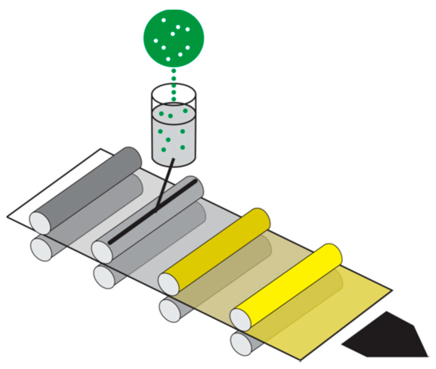
Silicon or sapphire wafers were used as a base for InGaN epitaxial deposition via Metal-Organic Chemical Vapour Deposition (MOCVD). The 450 nm wavelength emitting micro LED structures were then fabricated using a die mask set developed for this purpose. The 27 μm die segments were released into an ink binder (
Figure 1) and printed onto a 125 μm polyester substrate previously patterned with a micro silver metallic conductive. The nature of printing is statistical, in that the LED will have a random dispersion and orientation. The statistical electronics model assumes that printed devices fall into two groups; functional orientation or non-functional orientation and that there can be no other orientation. Statistical builds presuppose that devices are printed in functional areas and that, within a given area, the devices are wired in parallel where an individual device failure does not yield a function failure.
The initial LED designs had a random predominantly up/down orientation with a less likely sideways orientation. By refining the design of the micro LED, a shape was developed which would preferentially orientate in one direction.
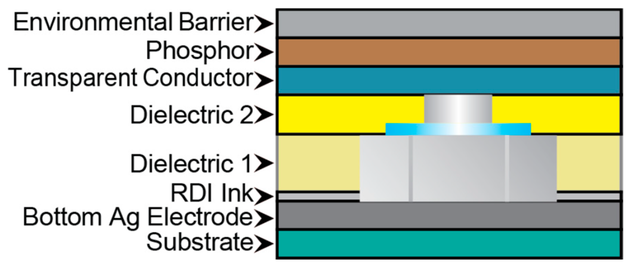
To complete the lamps, two transparent dielectric layers and a transparent conductive layer were added to make a vertically connected, randomly spaced diode array (
Figure 2). The phosphor layer is a doped yttrium-aluminium garnet (YAG) phosphor to convert the blue light produced by high bright LEDs into white light via a Stokes shift. No water or oxygen barrier is needed as these LEDs are inorganic. The environmental barrier layer was added to prevent mechanical damage to the YAG phosphor.
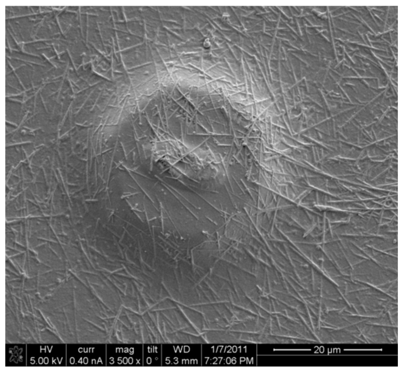
A scanning electron microscope (SEM) image of the resulting printed 27 μm die with the printed nano fibre transparent conductor, just prior to the phosphor lay down, is shown in
Figure 3. The silver nano fibre transparent conductor was developed to provide high conductivity and flexibility.
3. Application to Wearable Technology
The concept of the “Thunderstorm dress” was to turn the wearer into a living representation of a thunderstorm, creating a flash in response to a clap. In 2010 this had been realised using electroluminescent elements to create a lightning flash in the panels of the dress. However, this required the wearer to carry bulky electronics and heavy batteries. While it was used in marketing videos and at exhibitions the high voltage and power consumption made this impractical as wearable technology.
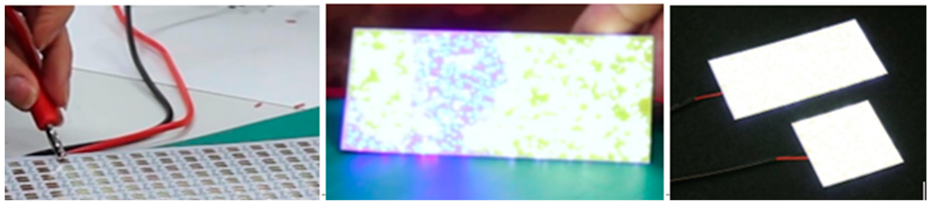
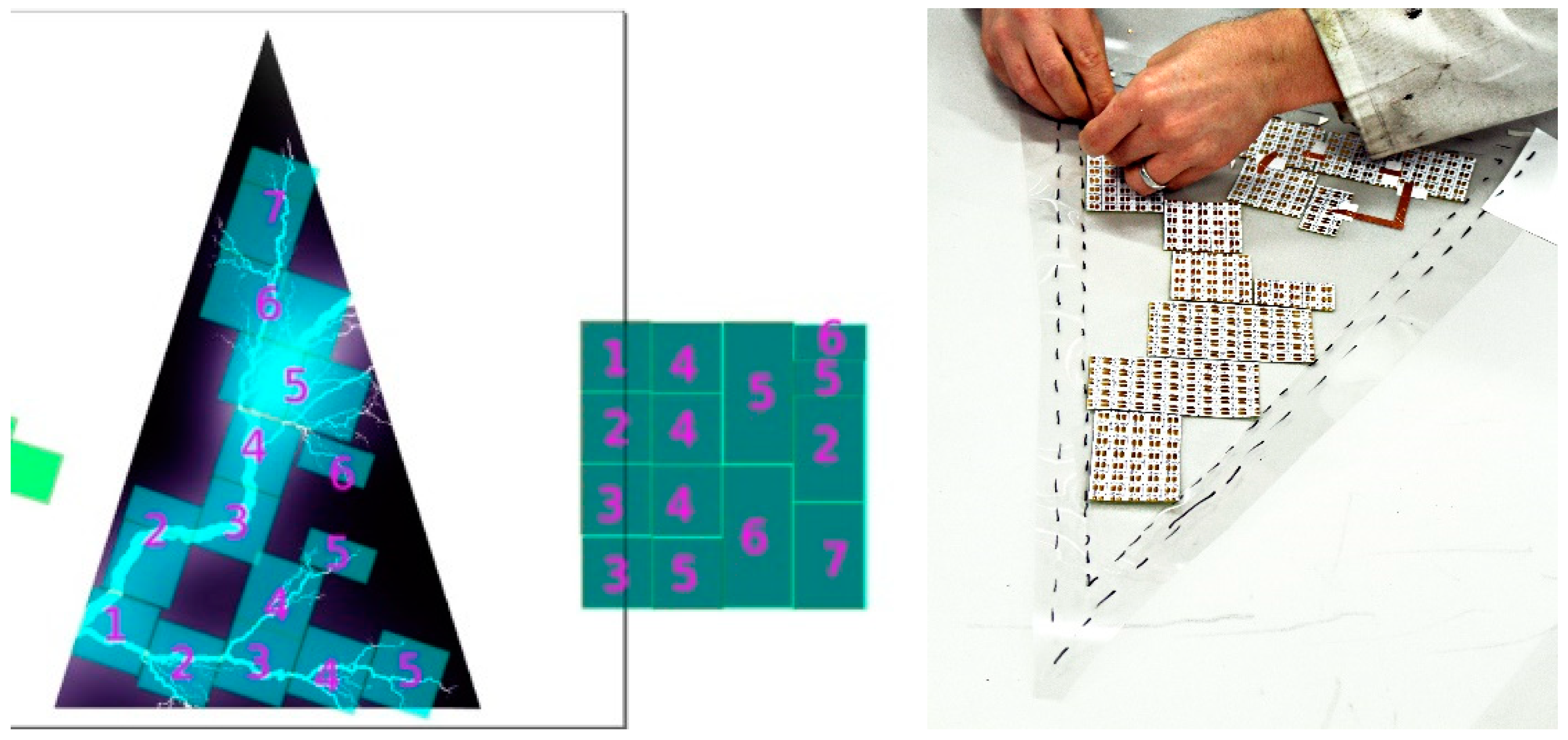
The opportunity to demonstrate the potential of this technology came when the Chicago Museum of Science and Industry commissioned the “Thunderstorm” dress for the 2019–2020 “Wired to Wear”, an exhibition focused on wearable technology. The inorganic printed micro LEDs afforded the potential to create a truly wearable piece of haute couture, using low voltages, miniature electronics and small batteries. The pattern of printed electrodes, micro LEDs and interconnects creates a seamless version which illuminates to the edge, so that butting panels together produces a continuous light. The pattern allows the individual panels, as shown in
Figure 4, to be cut to shape and then wired via any two terminals.
While the LEDs are ultra-bright, they produce distinct points of light, which require a diffuser to create a smooth illumination lamp. There was scope within the design of the dress to include a small air gap (2 mm) over the panel to allow the light to spread. The spacer also acted as a mask to limit the lit area. On top of this was attached a paper pattern containing the image of the flash (
Figure 5).
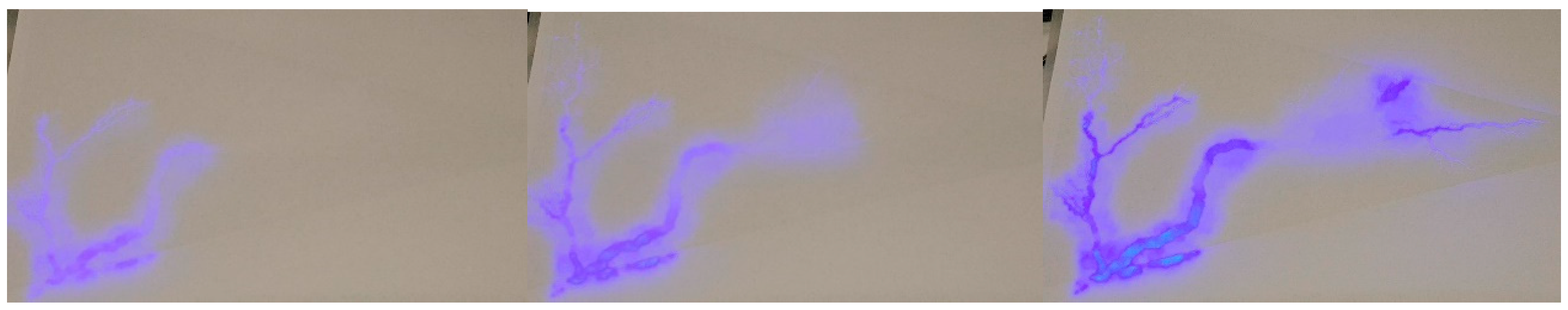
The lightning flash was created by assembling discrete lamps along the image, which could be individually addressed (
Figure 6). By cutting the LED sheet into smaller sections, it reduced the power requirements and in turn the size of the battery pack. A programmable control board designed for the wearable technology (Adafruit) was combined with power electronics to allow it to drive all 8 panels used simultaneously in the firing sequence indicated. By pulsing the power to the lamps, it was possible to build up the intensity to create a more realistic flash.
The paper panel highlighted the need to cut the outline of the mask more closely to the image and to improve the graphics. The primary aims of the graphics and the diffusing layers were; to increase diffusion of light so that the individual LEDs were not visible through the graphic; minimise the bleed through of light in undesired areas; hold enough rigidity to provide the dress with the fullness and volume to carry the sculptural aesthetics of the skirt, yet be soft enough for sewing and integration with the leather; and provide a high quality image with a leather-effect finish. Several different films and diffuser combinations were evaluated including PVC encapsulated paper and backlit polyester film. PVC was the most robust outcome. However, the light bleed was the poorest. The encapsulated paper gave the highest impact graphic but was the least robust. The backlit film with vinyl was selected for the final prototype to provide a leather-effect finish and acceptable light bleed. The improved flash can be seen on all 8 panels during testing prior to assembly into the garment (
Figure 7).
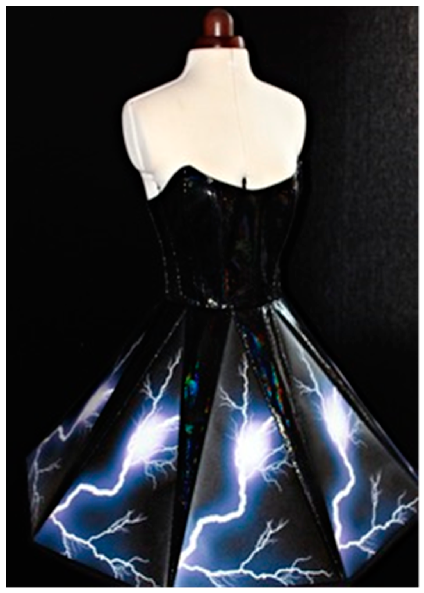
The garment was composed of a fitted holographic leather bodice and paneled circle skirt assembled from the eight electronic LED panels (
Figure 8). The integration of these LED electronic panels and the respective graphics layer was essential to the final assembly of the garment. This interaction between both the technology (LED panels) and the textile in the garment was fundamentally a compromise between the individual material qualities. To meet the requirements of the dress, the panels were chosen to be stiff enough to carry the sculptural aesthetics of the skirt but soft enough to be stitched and integrated with the leather. To match the stiffness of the graphics layer with the leather, a specialist interfacing was used, Vilene Decovil. The ’lightning’ graphic, therefore, was printed on a substrate which could transport the LEDs light source, was stitchable and matched the visual and tactile aesthetics of the holographic leather. The wiring harness and electronics were easily sewn into the dress without distorting the shape were incorporated into the design.
4. Conclusions
In contrast to the electroluminescent technology previously used, the printed LEDs provide a more mobile, lightweight, durable, low power and therefore safer solution for the high fashion Thunderstorm dress. An alternative route to the fabrication of printed electronics has been presented based on inorganic semiconductors dispersed in a conductive binder to create an ink. These axial lead micro LED devices can be accurately printed using conventional graphics processes (screen, flexography and gravure). This approach will act as a template for further development of inks and techniques for new devices that employ fabricated silicon or III-V semiconductors. This is now on display in the Museum of Science and Technology, Chigaco (MSI) in the 2019–2020 “Wired to Wear” exhibition.
The potential for these lightweight, flexible form factor lamps has been demonstrated by inclusion in a sound activated light emitting haute couture dress. This technology also has potential for application in flexible and display packaging.
