Proceeding Paper

UV Total Dose Nonvolatile Sensor Using Fluorine-Treated SOHOS Capacitor Device †

Department of Opto-Electronic System Engineering, Minghsin University of Science and Technology, Xinxing Road 1, Xinfeng 30401, Taiwan
Presented at the 4th International Electronic Conference on Sensors and Applications, 15–30 November 2017; Available online: http://sciforum.net/conference/ecsa-4.
Proceedings 2018, 2(3), 144; https://doi.org/10.3390/ecsa-4-04904
Published: 14 November 2017

Abstract

:
The fluorine-treated silicon–silicon oxide–hafnium oxide–silicon oxide–silicon capacitor device (hereafter F-SOHOS) could be a candidate for UV radiation total dose (hereafter TD) nonvolatile sensor. The UV radiation induces a significant increase in the threshold voltage VT of the F-SOHOS capacitor, and the change in VT for F-SOHOS capacitor also has a strong correlation to UV TD up to 100 mW·s/cm2 after UV irradiation. The experimental results indicate that UV TD radiation-induced increase of VT in F-SOHOS capacitor under gate positive bias stress (hereafter PVS) is nearly 4 V after UV TD 100 mW·s/cm2 irradiation. Moreover, the VT-retention loss of the nonvolatile F-SOHOS capacitor device after 10 years retention is below 15%. The UV TD data can be permanently stored and accumulated in the non-volatile F-SOHOS capacitor device. Furthermore, the UV TD data in the F-SOHOS capacitor devices can be erased to original null state by positive charges injection under gate negative bias stress (hereafter NVS). The F-SOHOS capacitor device in this study has demonstrated the feasibility of non-volatile UV TD radiation sensing.
Keywords:
UV; sensor; SOHOS; radiation; TD

1. Introduction

The measurement of Ultra-Violet (UV) irradiation total dose (hereafter TD) is very important in various UV radiation applications, such as biochemical technology, medical technology, industrial testing technology and semiconductor manufacturing technology. The semiconductor dosimeters offer many advantages, the dose sensing areas of semiconductor dosimeters are very small, and their dose sensitivity can be high in a small constrained space. A silicon–silicon dioxide–hafnium oxide–silicon dioxide–silicon (SOHOS) capacitor device has been shown to be suitable for nonvolatile UV irradiation TD sensor applications [1,2,3]. UV irradiation induces a significant increase in the threshold voltage VT of the SOHOS capacitor device and this UV induced increase in VT for SOHOS capacitor has a strong correlation to UV TD. Moreover, the reliability characteristic of VT retention for the SOHOS capacitor device is good, even after 10 years retention. This SOHOS UV TD sensor, has the following two characteristics: (1) The UV TD information can be stored and accumulated in this nonvolatile SOHOS capacitor device permanently, even under data read, data write, and high temperature condition [1,2,3,4,5,6,7,8]; (2) UV TD data in the SOHOS capacitor can be erased to original null state by positive charges injection under gate negative bias stress (hereafter NVS), but it can’t be annealed by high temperature [1,2,3,4,5,6,7,8].
The UV radiation–induced charging process in the SOHOS capacitor device is demonstrated as following: UV irradiation together with positive gate bias stress (hereafter PVS) was impinged simultaneously on the SOHOS capacitor device. Electrons from the valence band of Si substrate can be excited by UV photons and the UV irradiation induces ionized electron-hole pairs in silicon substrate of the SOHOS capacitor device. The survival yield of the electron-hole pairs (escape from the recombination after UV radiation excitation in the substrate) depends by electric field under gate PVS [9,10]. Under gate positive voltage stress (PVS), negative charges are injected from substrate into charge trapping layer and trapped in the charge-trapping layer of the nonvolatile SOHOS capacitor device. The build-up of negative charge changes the threshold voltage VT, and the VT shift depends on the absorbed TD of the UV irradiation. While the trapped electrons are hard to escape to the control gate due to the relatively higher barrier height of thick SiO2 blocking oxide. As a result, negative charges are accumulated permanently in the trapping layers of the SOHOS capacitor device.
However, the improvement of UV radiation–induced charging effect and charge-retention reliability characterization of a SOHOS capacitor device after UV irradiation has not been well studied; it is discussed in this study. A fluorine-treated silicon–silicon oxide–hafnium oxide–silicon oxide–silicon capacitor device (hereafter F-SOHOS) was proposed in this study. The UV radiation–induced charging effect and charge-retention reliability of the F-SOHOS capacitor devices were significant improved. The electrical performance of the F-SOHOS capacitor devices under various UV TD irradiation condition, including radiation-induced charge effect, and charge retention reliability, were the main subjects of this study. Figure 1a shows the cross-section view of the SOHOS capacitor devices. Figure 1b shows the charge generation and trapping states of the gate dielectric in the F-SOHOS capacitor device after UV irradiation.

2. Experiments

The F-SOHOS and SOHOS capacitor devices are prepared for this study. SOHOS capacitor structures were fabricated on p-type resistivity 15–25 ohm-cm Si <100> substrate. We used thermal SiO2 for the tunneling oxide, HfO2 films (100~200 nm) were deposited as the charge-trapping layers, CVD TEOS SiO2 for the blocking oxide of the gate dielectric, and low-pressure chemical vapor deposition (LPCVD) poly silicon for the gate material. The tunneling silicon oxide (SiO2) was formed on the wafers by an advanced clustered vertical furnace. After the tunneling oxide was formed, hafnium oxide (HfO2) films (100~200 nm) were deposited as the charge-trapping layers, with Hf(tert-butoxy)2(mmp)2 precursor in a metal organic chemical vapor deposition (MOCVD) system at 400~550 °C, on the SOHOS capacitor device. To manipulate the radiation-induced charging effects in F-SOHOS capacitor, two types of SOHOS capacitor devices were prepared: (1) SOHOS capacitor with standard HfO2 as the charge-trapping layer (hereafter STD-SOHOS); and (2) F-SOHOS capacitor, CF4 plasma treatment with 30 sccm at 50 W for 30 s was performed on SOHOS, both before and after HfO2 deposition. The SiO2–HfO2–SiO2 (hereafter OHO) gate stack consisted of a 1000 Å–2000 Å HfO2 and 50 Å–150 Å bottom and top silicon oxides. The poly silicon (200–400 nm) was formed by LPCVD for the control gate. For comparison, two types of the SOHOS capacitor devices had the same thickness of tunneling oxide, trapping oxide, and blocking oxide layer. Figure 1a shows the cross-section view of the SOHOS capacitor device.
Before UV TD data writing, gate negative bias stress (NVS) VG = −40 V was impinged on the SOHOS capacitor device to “erase” the native charge in the OHO trapping layer of the SOHOS capacitor device to null state by NVS. During UV TD data writing, UV irradiation (UV LED, wavelength 400 nm) together with a gate positive bias stress (PVS) were applied simultaneously on the SOHOS capacitor devices. The various UV irradiation and various gate PVS conditions applied simultaneously on the SOHOS capacitor devices are listed in Table 1. After UV TD data writing, VT was measured at room temperature using a HP4156A parameter analyzer. The experimental results of gate capacitance applied at various gate voltages (CG-VG) were obtained by a computer-controlled HP4284 parameter analyzer, and the CG-VG curves were measured by sweeping VG at room temperature. Figure 1b shows the charge generation and trapping states of the gate dielectric in the F-SOHOS capacitor device after UV irradiation.

3. Results and Discussion

3.1. Radiation-Induced VT Shift in F-SOHOS after UV Irradiation
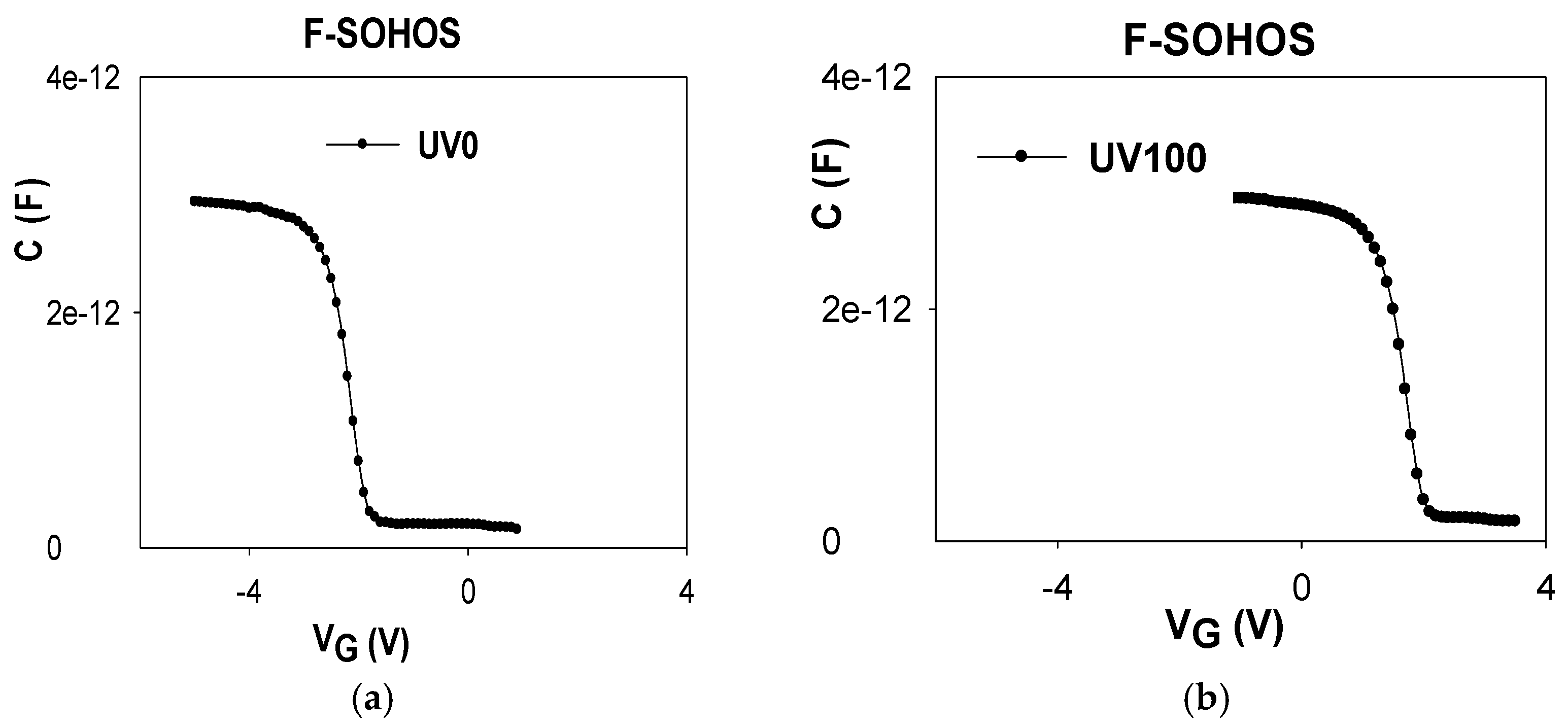
Figure 2a shows a CG-VG curve for a F-SOHOS capacitor device before UV irradiation. Before UV TD data writing, gate NVS (VG = −40 V) was impinged on the F-SOHOS capacitor device to “erase” the native charge in the OHO trapping layer and the F-SOHOS capacitor device is in erased state before UV irradiation. So, the curve shown in Figure 2a is the curve for a F-SOHOS capacitor device after gate NVS (VG = −40 V). Figure 2b shows a CG-VG curve for a F-SOHOS capacitor device after 100 mW·s/cm2 TD UV irradiation under PVS (VG = 20 V). For UV TD data writing, 100 mW·s/cm2 TD UV irradiation together with PVS (VG = 20 V) were impinged simultaneously on the F-SOHOS capacitor devices. As illustrated in Figure 2b, the CG-VG curve of F-SOHOS capacitor shifted to the right after UV total dose (here after TD) up to 100 mW·s/cm2 irradiation under gate PVS 20 V. This indicates that UV TD 100 mW·s/cm2 irradiation induces a increase of VT (about 4 V) for the F-SOHOS capacitor under gate PVS VG 20 V. This positive VT shift result is in agreement with previous studies [1,2,3].
The positive VT shift is due to an increase in net total negative trapped charges accumulated in the OHO gate dielectric layer after UV TD irradiation under gate PVS 20 V. These radiation-induced positive VT shifts in the UV irradiated F-SOHOS capacitor device under gate PVS 20 V are result from electrons on Si substrate excited by UV photons, and then injected under gate PVS 20V over the Si-SiO2 potential barrier into the trapping layer, and finally trapped in the nitride trapping layer of OHO [1,2,3]. UV TD irradiation and gate PVS was applied on the F-SOHOS capacitor device simultaneously for writing data by UV radiation. When the F-SOHOS capacitor structures are irradiated by UV TD irradiation, electrons from silicon substrate can be excited by UV photons. These free carriers are swept by electric field under gate PVS over the Si-SiO2 potential barrier and injected into the OHO gate dielectric layer, and some of these carriers are captured by the charge trap centers in OHO trapping layer. The UV radiation writing induces significant increase of threshold voltage for F-SOHOS capacitor devices. It is considered that this threshold change mostly owing to significant increase of electron trapped charges in the gate dielectric OHO after UV TD data writing. The change of gate threshold voltage in this case can be correlated to the amount of trapped charges and the exposure TD of UV radiation as well. These trapped charges are accumulated in gate dielectric layer, so UV TD record can’t be destroyed or disturbed by UV TD data write and read. For the erase of UV TD data, data in the SOHOS capacitor devices can be erased to original null state by positive charges injection under NVS.
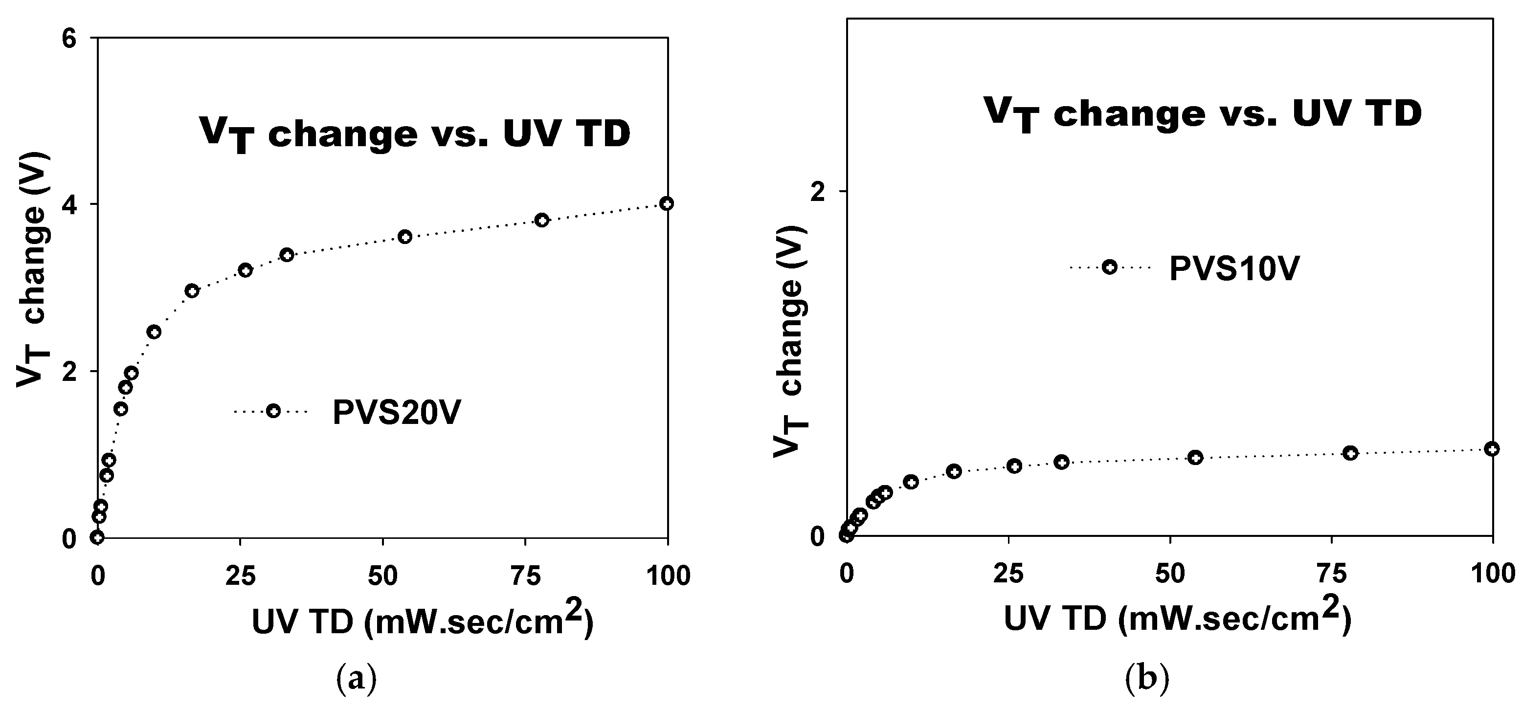
The VT increase are plotted against the UV irradiation TD for F-SOHOS capacitors under PVS 20 V and PVS 10 V as shown in Figure 3a,b, respectively. The VT increase as a function of UV TD for F-SOHOS capacitors device under PVS 20 V are shown in Figure 3a. The increase in F-SOHOS VT can be correlated to the increase in UV TD. But the VT increased more slowly when UV TD larger than 30 mW·s/cm2. These experimental results in this study are in agreement with previous studies [1,2,3].
The dependence of the VT shift on UV TID for F-SOHOS capacitor under PVS 20 V was more obvious than that under gate PVS 10 V as shown in Figure 3a,b. Under higher gate PVS, electrons are swept by higher electric field under higher gate PVS and more electrons were captured by more charge trap centers of OHO trapping layer.
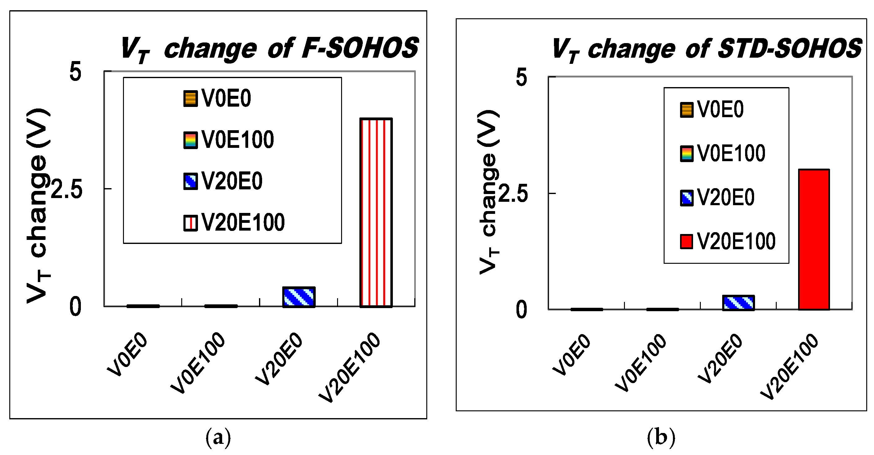
The comparisons of VT increase of two types of SOHOS capacitor devices after various UV irradiation conditions are shown in Figure 4a,b. The symbol list for various UV and PVS condition on SOHOS capacitor device are listed in Table 1. As illustrated in Figure 4a,b, the change of threshold voltage of SOHOS capacitor was ignorable with only UV TD irradiation conditions (without gate PVS), and also ignorable with only gate PVS conditions (without UV TD irradiation). It is considered that both UV TD irradiation and gate PVS should be applied on the SOHOS capacitor device simultaneously for writing UV TD radiation data, and the significant increase of threshold voltage is due to an significant increase of electron trapped charges in the gate dielectric OHO layer after UV TD irradiation and gate PVS simultaneously. As shown in Figure 4a,b, it is noted that the UV TD radiation-induced VT increase of the F-SOHOS capacitor device was nearly 1.5 times larger than that of the STD-SOHOS capacitor device after 100 mW·s/cm2 UV TD irradiation under 20 V VG PVS. The UV TD radiation-induced VT shift of F-SOHOS capacitor is more significant than that of STD-SOHOS capacitor as shown in Figure 4a,b, which results from the amount of UV TD radiation-induced charge trapped in the F-SOHOS capacitor is greater than that in the STD-SOHOS capacitor under gate PVS. The F-SOHOS capacitor device with larger F-treatment volume in HfO2 has the higher UV radiation-induced charge density than the STD-SOHOS capacitor devices after UV irradiation. For comparison, two type of the SOHOS capacitor devices had the same thickness of tunneling oxide, trapping nitride, and blocking oxide layer.

3.2. VT Stability vs. Retention Time
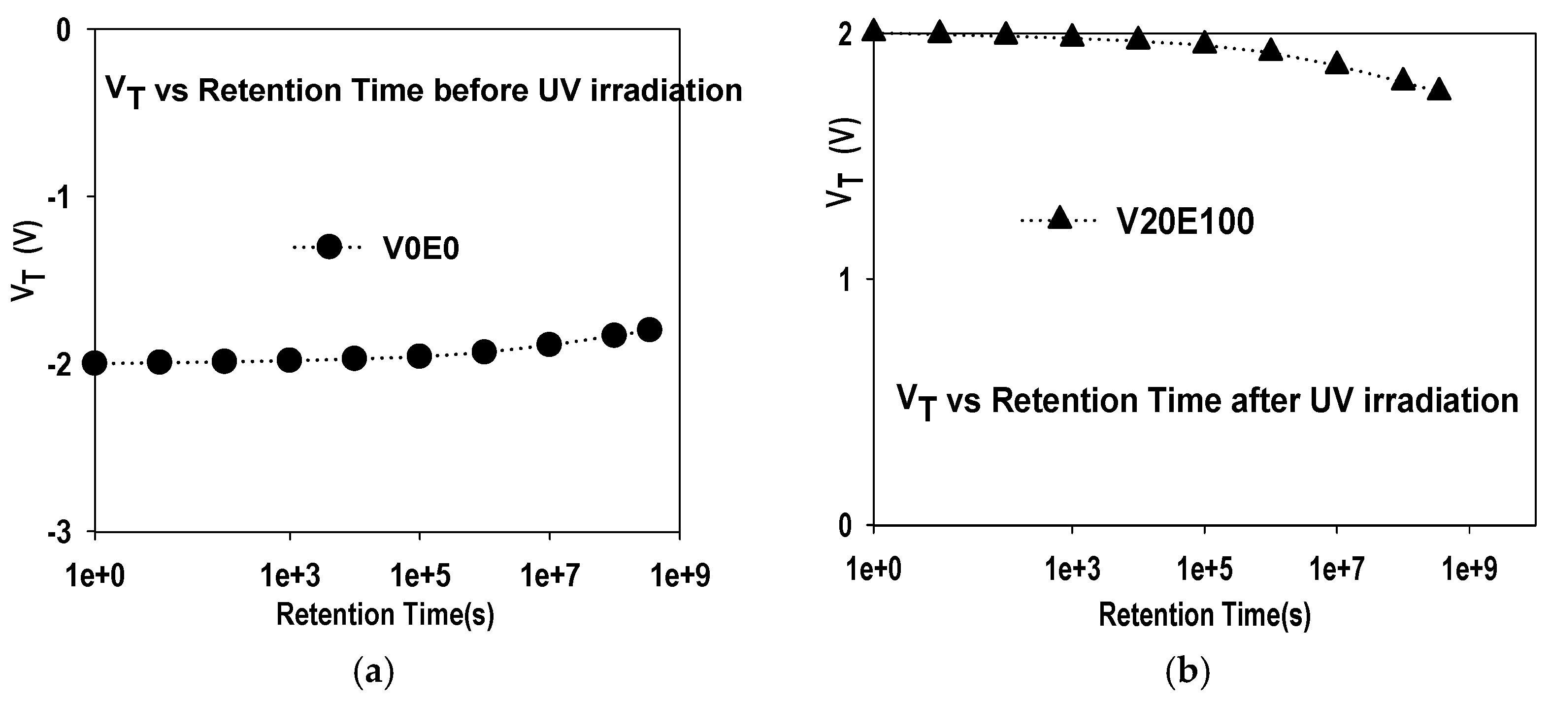
The VT vs. retention time for an F-SOHOS capacitor device before and after UV 100 mW·s/cm2 irradiation under PVS 20 V are illustrated in Figure 5a,b, respectively. As illustrated in Figure 5a, the increase in VT with time for the pre-UV-irradiated F-SOHOS capacitor device is a result of negative charges naturally tunneling into the HfO2 trapping layer of F-SOHOS device before UV irradiation. As shown in Figure 5b, the decrease in the VT with time for the post-UV-irradiated F-SOHOS capacitor device is a result of UV radiation-induced negative charges tunneling out from the HfO2 trapping layer. Moreover, the VT-retention loss of the nonvolatile F-SOHOS capacitor device after 10 years retention is below 15%. For F-SOHOS type nonvolatile device, the electrons in trapping layer are hard to escape to the control gate due to the relatively higher barrier height of thick SiO2 blocking oxide. As a result, negative charges are accumulated permanently in the layers.
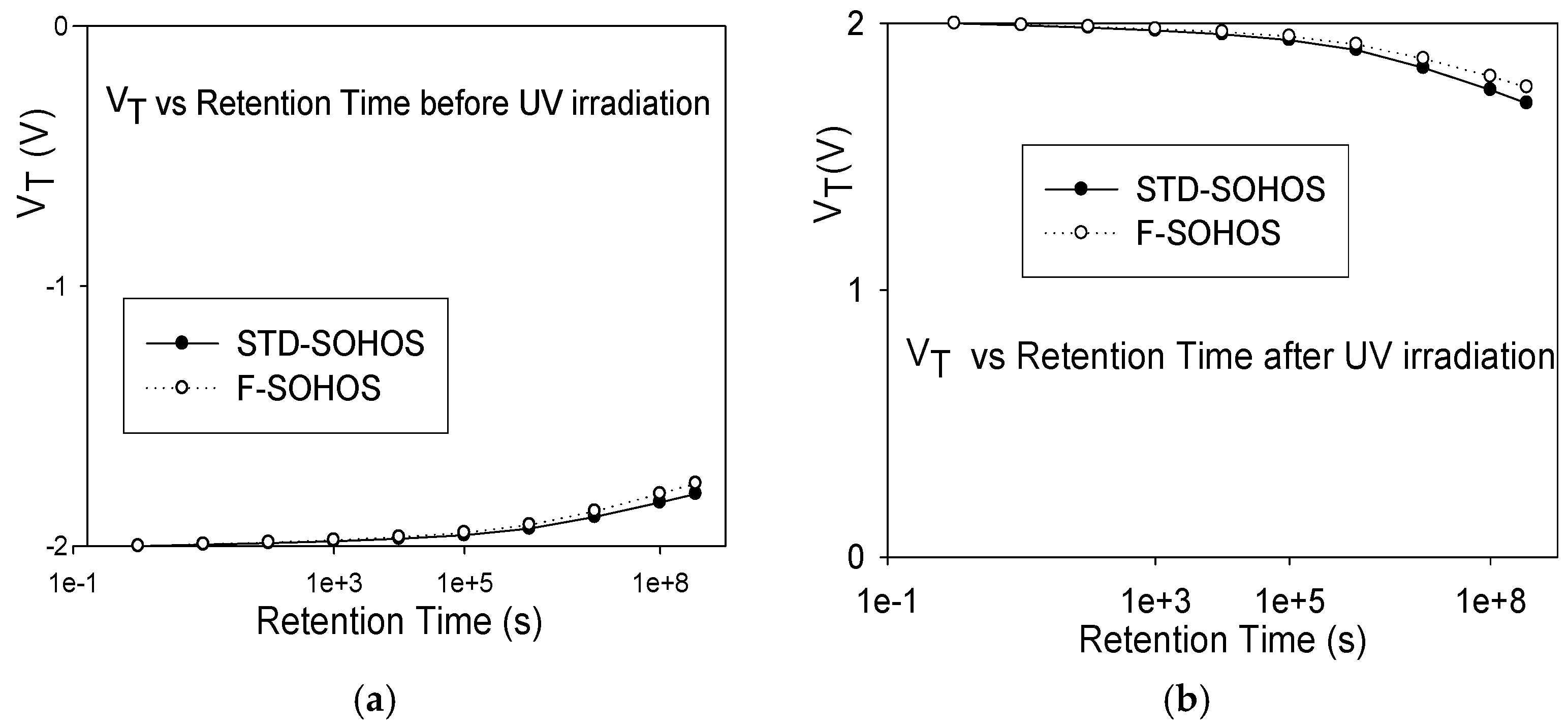
Figure 6a,b show the comparison of the charge retention reliability characteristics of two types of SOHOS capacitor devices before UV irradiation and after UV 100 mW·s/cm2 irradiation under PVS 20 V. However, an F-SOHOS demonstrated better UV induced charge-retention reliability characteristics than STD-SOHOS. This result also agreed with the previous study of an F-SOHOS device [5,10]. A much deeper charge trap energy level (ETA) was observed for an F-SOHOS with fluorine-treated hafnium oxide trapping layer than that for STD-SONOS in the previous study [5,10]. Therefore, the F-SOHOS device with deeper charge traps in the fluorine-treated hafnium oxide trapping layer showed better UV induced charge-retention reliability characteristics than the STD-SOHOS devices. The charge-retention loss of the nonvolatile F-SOHOS capacitor after 10 years retention is below 15%. The nonvolatile F-SOHOS capacitor devices have very good reliability characteristics of VT retention, even for 10 years. The UV TD information can be permanently stored and accumulated in the non-volatile F-SOHOS capacitor devices.

4. Conclusions

As shown in experiment data, the VT increase of the F-SOHOS capacitor was nearly 4 V, and was 1.3 times larger than that of the STD-SOHOS capacitor after 100 mW·s/cm2 UV TD irradiation under 20 V VG PVS. The UV induced change in VT for F-SOHOS capacitor also has a strong correlation to UV TD up to 100 mW·s/cm2 irradiation. But the VT of F-SOHOS capacitor was not changed obviously with 100 mW·s/cm2 UV TD irradiation only (without gate PVS) or with 20 V gate PVS only (without UV irradiation) conditions. Moreover, the F-SOHOS devices with deeper charge traps in the fluorine-treated hafnium oxide trapping layer showed better UV induced charge-retention reliability characteristics than the STD-SOHOS devices. The 100 mW·s/cm2 UV induced charge-retention loss of the nonvolatile F-SOHOS capacitor after 10 years retention is below 15%. The F-SOHOS capacitor device in this study has demonstrated the feasibility of non-volatile UV TD radiation sensing.

Acknowledgments

The author thanks the National Nano Device Laboratories (NDL), National Tsing Hua University (NTHU), and National Chiao Tung University (NCTU) for providing the instruments for wafer fabrication and testing. This study was funded in part by the National Science Council (NSC).

References

  1. Hsieh, W.C.; Lee, H.D.; Jong, F.C.; Wu, S.C. UV Nonvolatile Sensor by Using SONOS Capacitor Device. In Proceedings of the 2013 6th IEEE International Conference on Advanced Infocomm Technology (ICAIT), Hsinchu, Taiwan, 6–9 July 2013. [Google Scholar]
  2. Roizin, Y.; Gutman, M. Plasma-Induced Charging in Two Bit per Cell SONOS Memories. In Proceedings of the 8th IEEE International Symposium on IEEE Plasma- and Process-Induced Damage, Corbeil-Essonnes, France, 24–25 April 2003. [Google Scholar]
  3. Abraham, A.; Nicola, N.; Diana, N.; Curiel, M. MOS Structures Containing Si Nanocrystals for Applications in UV Dosimeters. Key Eng. Mater. 2014, 605, 380. [Google Scholar] [CrossRef]
  4. Hsieh, W.C.; Lee, H.D.; Jong, F.C. An Ionizing Radiation Sensor Using a Pre-Programmed MAHAOS Device. Sensors 2014, 14, 14553–14566. [Google Scholar] [CrossRef] [PubMed]
  5. Hsieh, W.C.; Lee, H.D.; Jong, F.C.; Wu, S.C. An Performance Improvement of Total Ionization Dose Radiation Sensor Devices Using Fluorine-Treated MOHOS. Sensors 2016, 16, 450. [Google Scholar] [CrossRef] [PubMed]
  6. Hsieh, W.C.; Lee, H.D.; Jong, F.C.; Wu, S.C. Effect of N Implantation on the Performance of TOHOS Total Ionizing Dose Radiation Sensor Device. Sens. Mater. 2016, 5, 577–584. [Google Scholar]
  7. Hsieh, W.C.; Lee, H.D.; Jong, F.C.; Wu, S.C. Charge Retention Improvement of Nonvolatile Radiation Sensor Using MONOS with Si-rich Nitride and Oxy-Nitride as Stack Charge-Trapping Layer. Sens. Mater. 2016, 9, 1023–1033. [Google Scholar]
  8. Oldham, T.R.; McLean, F.B. Total Ionizing Dose Effects in MOS Oxides and Devices. IEEE Trans. Nucl. Sci. 2003, 50, 483–499. [Google Scholar] [CrossRef]
  9. Cheng, Y.; Ding, M.; Wu, X.; Liu, X.; Wu, K. Irradiation effect of HfO2 MOS structure under gamma-ray. In Proceedings of the 2013 International Conference Solid Dielectrics, Bologna, Italy, 30 June–4 July 2013; pp. 764–767. [Google Scholar]
  10. Wu, W.C.; Lai, C.S.; Wang, T.M.; Wang, J.C.; Hsu, C.W.; Ma, M.W.; Lo, W.C.; Chao, T.S. Carrier Transportation Mechanism of the TaN/HfO2/IL/Si Structure with Silicon Surface Fluorine Implantation. IEEE Trans. Electron Devices 2008, 55, 1639–1646. [Google Scholar] [CrossRef]
Figure 1. (a) Cross-sectional view of an SOHOS capacitor device; (b) Charge generation and trapping in the F-SOHOS capacitor after UV irradiation.
Proceedings 02 00144 g001
Figure 2. This CG-VG curve for an F-SOHOS capacitor device (a) before UV irradiation; (b) after UV TD 100 mW s/cm2 irradiation.
Proceedings 02 00144 g002
Figure 3. The dependence of the VT increase on UV irradiation TD for an F-SOHOS capacitor (a) under gate PVS 20V; (b) under gate PVS 10 V.
Proceedings 02 00144 g003
Figure 4. (a) The VT change of F-SOHOS capacitor devices after various UV irradiation; (b) The VT change of STD-SOHOS capacitor devices after various UV irradiation.
Proceedings 02 00144 g004
Figure 5. The VT vs. retention time for an F-SOHOS device: (a) before UV irradiation; and (b) after UV TD 100 mW·s/cm2 irradiation under gate PVS 20V.
Proceedings 02 00144 g005
Figure 6. The comparison of VT vs. retention time for F-SOHOS and STD-SOHOS devices: (a) before UV irradiation; (b) after UV TD 100 mW·s/cm2 irradiation under gate PVS 20 V.
Proceedings 02 00144 g006
Table 1. Symbol list for various UV TD and PVS conditions applied simultaneously on F-SOHOS.
SymbolUV TD (mW·s/cm2)PVS VG (V)
V0E0 0 mW·s/cm20 V
V0E100100 mW·s/cm20 V
V20E00 mW·s/cm220 V
V20E100100 mW·s/cm220 V
Publisher’s Note: MDPI stays neutral with regard to jurisdictional claims in published maps and institutional affiliations.

