Proceeding Paper

Epitaxial Graphene Sensors Combined with 3D Printed Microfluidic Chip for Heavy Metals Detection †

by
Maria Francesca Santangelo
1,*,
Ivan Shtepliuk
2,
Donatella Puglisi
1,
Daniel Filippini
3,
Rositsa Yakimova
2,4 and
Jens Eriksson
1
1
Applied Sensors Science, Department of Physics, Chemistry, and Biology—IFM, Linköping University, S-58183 Linköping, Sweden
2
Semiconductor Materials, Department of Physics, Chemistry, and Biology—IFM, Linköping University, S-58183 Linköping, Sweden
3
Optical Devices Laboratory, Department of Physics, Chemistry, and Biology—IFM, Linköping University, S-58183 Linköping, Sweden
4
GraphenSiC AB, SE-58330 Linköping, Sweden
*
Author to whom correspondence should be addressed.
Presented at the Eurosensors 2018 Conference, Graz, Austria, 9–12 September 2018.
Proceedings 2018, 2(13), 982; https://doi.org/10.3390/proceedings2130982
Published: 30 November 2018
(This article belongs to the Proceedings of EUROSENSORS 2018)

Abstract

:
Two-dimensional materials may constitute key elements in the development of a sensing platform where extremely high sensitivity is required, since even minimal chemical interaction can generate appreciable changes in the electronic state of the material. In this work, we investigate the sensing performance of epitaxial graphene on Si-face 4H-SiC (EG/SiC) for liquid-phase detection of heavy metals (e.g., Pb). The integration of preparatory steps needed for sample conditioning is included in the sensing platform, exploiting fast prototyping using a 3D printer, which allows direct fabrication of a microfluidic chip incorporating all the features required to connect and execute the Lab-on-chip (LOC) functions. It is demonstrated that interaction of Pb2+ ions in water-based solutions with the EG enhances its conductivity exhibiting a Langmuir correlation between signal and Pb2+ concentration. Several concentrations of Pb2+ solutions ranging from 125 nM to 500 µM were analyzed showing good stability and reproducibility over time.

1. Introduction

Nowadays, among water pollutants, heavy metals (HMs) are considered as the most serious source to pollute the biosphere, posing a significant threat to human health, because they are non- biodegradable and can be accumulated in soft tissues [1]. Some HMs are essential minerals for healthy biochemical and physiological function, since they serve as components of several key enzymes and play important roles in various oxidation-reduction reactions in human bodies. Others, such as lead, chromium, arsenic, and mercury are toxic even when ingested in very small quantities [2]. This has led the scientific community to develop simple methods towards their accurate and sensitive identification in the environment. Graphene is one of the best transducer materials because it exhibits extreme sensitivity thanks to its unique properties, such as every atom being available for interaction with adsorbing molecules, the high carrier mobility, and the high electronic conductivity even when very few charge carriers are present [3]. As a result, very small changes in e.g., conductivity can be detected leading to high-resolution sensors. Driven by these features, we investigated the performance of a sensing platform based on epitaxial graphene on Si-face 4H-SiC (EG/SiC) for liquid- phase detection of HMs, simply measuring the conductivity changes due to the interaction between ions and the sensing surface. In this work, we developed and tested a reusable lab-on-chip for heavy metals detection, in which the 3D printed microfluidic cell allowed the interaction between the HMs solutions and the sensing surface. Moreover, Density Functional Theory (DFT) calculations were performed to explain the interaction mechanism between graphene and lead ions and consequentially conductivity changes of the sensing material.

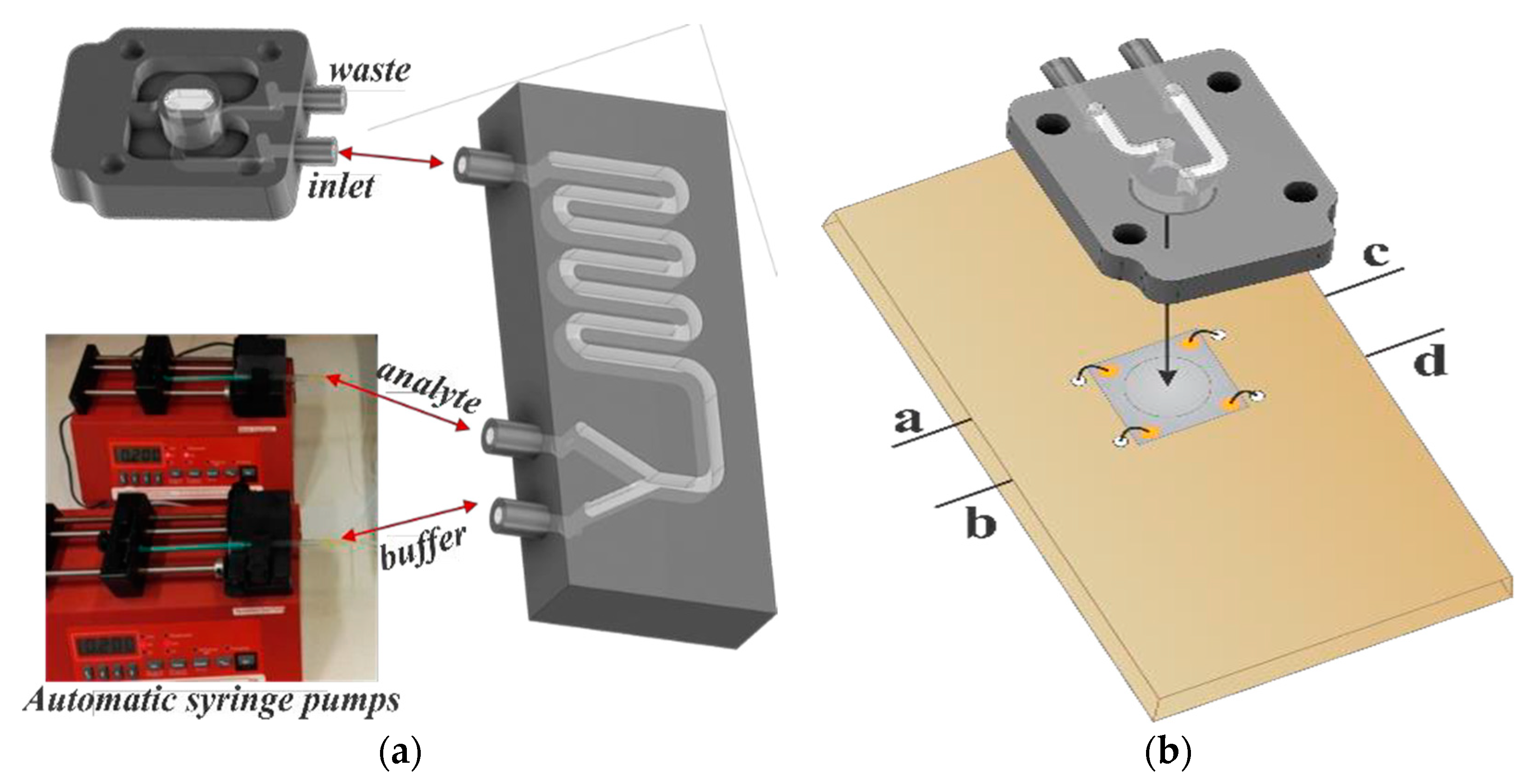
2. Materials and Methods

In this work, an EG-based device (7 mm × 7 mm) coupled to a 3D printed microfluidic chip with a chamber volume of 7 µL was employed, as shown in Figure 1. Graphene monolayer was grown on 4H-SiC (0 0 0 1) substrate in an inductively heated furnace under isothermal conditions at a temperature of 2000 °C in argon environment with a pressure of 1 atm [4]. Four circular (θ = 1 mm) contacts were fabricated on the graphene through sputter deposition of 2 nm of titanium and 200 nm of gold sequentially [5]. Four-point measurements are possible with this scheme, but only resistance between a and d (Figure 1) was measured in this case. The chamber was fixed on the EG surface, and thanks to the pressure applied using four screws that fix the chip to the board, the chamber was perfectly sealed. Analyte solutions, with concentrations of lead ions (Pb2+) ranging from 125 nM to 500 µM, were prepared diluting a powder of lead chloride, PbCl2 (purchased from Sigma-Aldrich) in deionized water (dH2O), and injected into an external microfluidic chip in which mixing between the buffer solution (dH2O) and analyte (Pb2+) takes place, thanks to the presence of a bulk serpentine [6]. Both solutions were injected using two automatic syringe pumps (NE-1010 Higher Pressure Programmable Single Syringe Pumps) with a flow-rate of 19.2 mL/h. Buffer solution was used both to dilute the analyte concentration and to clean the chip after each measurement cycle. Both microfluidic chips, which include inlet and outlet ports with an internal radius of 500 µm, were designed using Autodesk Inventor Fusion 360® CAD software (version 2.0.5044) and printed by a Form 1 + 3D printer (FormLabs) with a proprietary resin Clear Type 02. The resin includes different proportions of modified acrylate and acrylate oligomer, epoxy monomer, acrylate monomer, photo initiator and additives as the principal components [7,8]. A 2601A Keithley Source Meter was used to bias the sensor ant to collect the output signal.

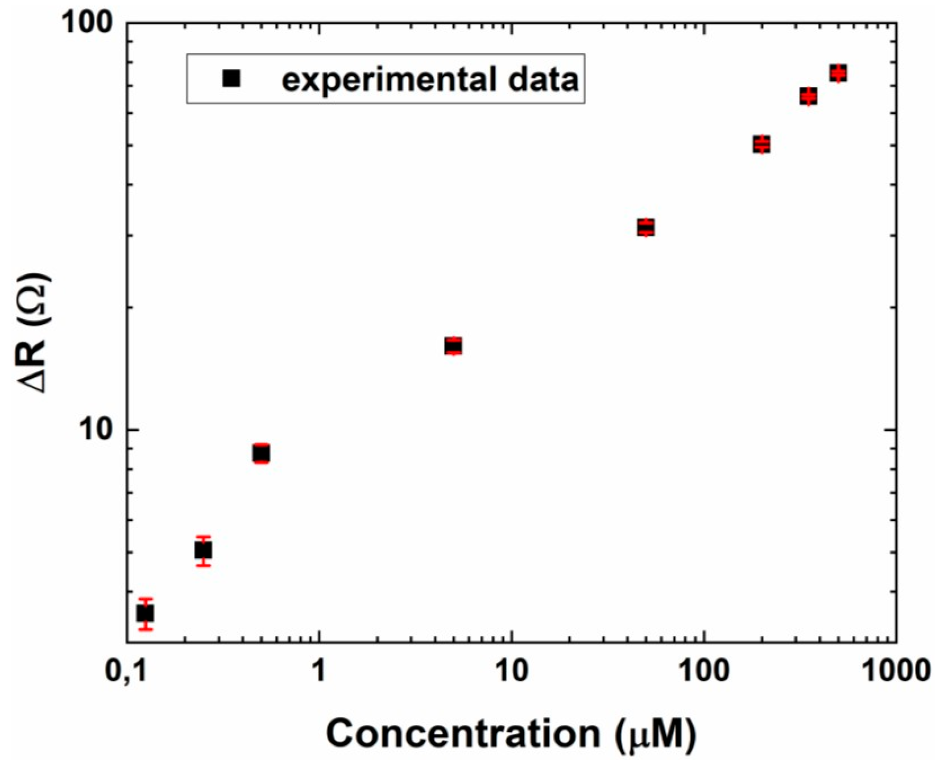
3. Results and Discussion

Density Functional Theory calculations performed indicate that Pb2+ ions, adsorbed on graphene, behave as electron-accepting dopants, with a preferential charge transfer from graphene to divalent ions. This process of energy transfer produces a change in the graphene conductivity, which was confirmed by our experimental measurements. Indeed, starting from PbCl2 diluted in dH2O, several concentrations of Pb2+ solutions ranging from 125 nM to 500 µM were measured. Since the water molecules on graphene act as electron-accepting (p-type) dopants [9], we observed that the presence of charged lead species in water electrolyte increased the p-type conductivity of graphene. For each concentration of Pb2+ more than three measurement cycles were measured and the differential resistance (ΔR) and experimental error were calculated and reported in Figure 2. In particular, the resistance value reported (ΔR) is the net resistance measured as the difference between the signal due to the presence of Pb2+ and the recovery value obtained by cleaning of the chip after each measurement cycle.
In particular, in accordance with Langmuir’s law, which describes the adsorption of species onto simple surfaces, increasing the Pb2+ concentration leads to increase of ΔR value (Figure 2), since more divalent ions are adsorbed on the EG surface. Moreover, DFT calculations indicate that for high level of Pb2+ concentration, the energy transfer between individual lead ions and graphene decreases. It has also been confirmed by the experimental data, since we obtained two different sensitivities for low and high Pb2+ concentration, as demonstrated by the two different slopes of the calibration curve reported in Figure 2. In particular, it was observed that for low concentration of Pb2+ the system exhibits a sensitivity (SL = 13.90 Ω/µM) that is much higher than that one (SH = 0.10 Ω/µM) obtained for high concentration of Pb2+. This result demonstrates how the system is more sensitive to low concentrations of the analyte. Moreover, a detection limit of 95 nM was extrapolated from the calibration curve, which is much lower than the recommended safe limit (180 nM) provided by the World Health Organization (WHO) [10] for lead levels in drinking water. This value can be still improved increasing the area of the graphene surface exposed to the HMs solution.

4. Conclusions

In this work we showed design and testing of a new sensing platform based on epitaxial graphene sensor coupled to 3D printed microfluidic chip for heavy metals detection. The use of an EG sensor and a 3D printed microfluidic chip allowed the detection of low traces of Pb2+ due to the extreme sensitivity of the material and the reduction of reactants consumption, respectively. A detection limit of 95 nM was obtained, which is much lower than the recommended limit provided by WHO for Pb levels in drinking water, and it can be still improved increasing the EG area exposed to the solution. DFT calculations indicated that the presence of Pb2+ ions absorbed on graphene increases the p-type conductivity producing an increase of the differential resistance and were confirmed by experimental data. In particular the extreme sensitivity of the system to a low level of Pb2+ concentration was demonstrated. All the features described in this work show that this system can be used for accurate and sensitive identification of heavy metals in the environment.

Author Contributions

The manuscript was written through contributions of all authors. All authors have given approval to the final version of the manuscript. The authors contributed equally.

Acknowledgments

The authors would like to thank the Swedish Foundation for Strategic research (SSF) for funding support through the grants GMT14-0077 and RMA15-024. We acknowledge support from the Swedish Government Strategic Research Area in Materials Science on Functional Materials at Linköping University (Faculty Grant SFO-Mat-LiU # 2009-00971).

Conflicts of Interest

The authors declare no conflict of interest.

References

  1. Cui, L.; Wu, J.; Ju, H. Electrochemical sensing of heavy metal ions with inorganic, organic and bio-materials. Biosens. Bioelectron. 2015, 63, 276–286. [Google Scholar] [CrossRef] [PubMed]
  2. Available online: https://www.hydroviv.com/blogs/water-smarts/heavy-metal-toxicity (accessed on 29 November 2018).
  3. Novoselov, K.S.; Geim, A.K.; Morozov, S.V.; Jiang, D.; Zhang, Y.; Dubonos, S.V.; Grigorieva, I.V.; Firsov, A.A. Electric Field Effect in Atomically Thin Carbon Films. Science 2004, 306, 666–669. [Google Scholar] [CrossRef] [PubMed]
  4. Yazdi, G.R.; Vasiliauskas, R.; Iakimov, T.; Zakharov, A.; Syväjärvi, M.; Yakimova, R. Growth of large area monolayer graphene on 3C-SiC and a comparison with other SiC polytypes. Carbon 2013, 57, 477–484. [Google Scholar] [CrossRef]
  5. Rodner, M.; Bahonjic, J.; Mathisen, M.; Gunnarsson, R.; Ekeroth, S.; Helmersson, U.; Ivanov, I.G.; Yakimova, R.; Eriksson, J. Performance tuning of gas sensors based on epitaxial graphene on silicon carbide. Mater. Des. 2018, 153, 153–158. [Google Scholar] [CrossRef]
  6. Comina, G.; Suska, A.; Filippini, D. Towards autonomous lab-on-a-chip devices for cell phone biosensing. Biosens. Bioelectron. 2016, 77, 1153–1167. [Google Scholar] [CrossRef] [PubMed]
  7. Comina, G.; Suska, A.; Filippini, D. Low cost lab-on-a-chip prototyping with a consumer grade 3D printer. Lab Chip 2014, 14, 2978–2982. [Google Scholar] [CrossRef] [PubMed]
  8. Santangelo, M.F.; Libertino, S.; Turner, A.P.F.; Filippini, D.; Mak, W.C. Integrating printed microfluidics with silicon photomultipliers for miniaturised and highly sensitive ATP bioluminescence detection. Biosens. Bioelectron. 2018, 99, 464–470. [Google Scholar] [CrossRef] [PubMed]
  9. Leenaerts, O.; Partoens, B.; Peeters, F.M. Adsorption of H2O, NH3, CO, NO2, and NO on graphene: A first-principles study. Phys. Rev. B 2018, 77, 125416. [Google Scholar] [CrossRef]
  10. Available online: http://www.who.int/water_sanitation_health/dwq/chemicals/lead.pdf (accessed on 29 November 2018).
Figure 1. (a) Schematic of the sensing platform; (b) Description of mounting process based on 7 mm × 7 mm EG- based device coupled to 3D printed microfluidic chip.
Proceedings 02 00982 g001
Figure 2. Calibration curve: experimental data (black squares) and relative error bars (red lines).
Proceedings 02 00982 g002
Publisher’s Note: MDPI stays neutral with regard to jurisdictional claims in published maps and institutional affiliations.

