Proceeding Paper

An LED Platform for Micropower Gas Sensors †

1
MIND-IN2UB, Department of Electronic and Biomedical Engineering, Universitat de Barcelona, E-08028 Barcelona, Spain
2
IHT-LENA, Technische Universität Braunschweig, D-38106 Braunschweig, Germany
*
Author to whom correspondence should be addressed.
Presented at the Eurosensors 2018 Conference, Graz, Austria, 9–12 September 2018.
Proceedings 2018, 2(13), 971; https://doi.org/10.3390/proceedings2130971
Published: 30 November 2018
(This article belongs to the Proceedings of EUROSENSORS 2018)

Abstract

:
We developed an integrated platform to build up conductometric sensors with controlled illumination. Our device contains a miniaturized indium gallium nitride (InGaN) LED as a light source, and a set of interdigitated electrodes (IDEs) in close contact with the LED. The sensor material is later deposited on top of the IDE, to monitor its resistance. In this configuration, all the light emitted by the LED is collected by the sensor material, leading to a very efficient photoexcitation. We demonstrate the effectiveness of the approach building a photoactivated gas sensor based on ZnO operating with as little as 100 μW.

1. Introduction

Controlled excitation is required in many sensing applications based on physicochemical properties of materials. For example, in conductometric gas sensors, the response to gases of a given semiconductor material is usually activated with heat or with light. In the former case, power consumption due to the need of heating is an issue. Even with the most advanced microfabricated heaters, typical power consumptions fall in the range of several to tens of milliwatts [1]. In the latter case, there have been many efforts to combine LED sources in sensors, but always based on hybrid integration of discrete LED dices in a mini/micro system. Due to the spreading of light with the distance, such approach is not very efficient. In this work, we aimed at integrating, for the first time, a monolithic device embodying the LED, the IDEs, and the sensor material.

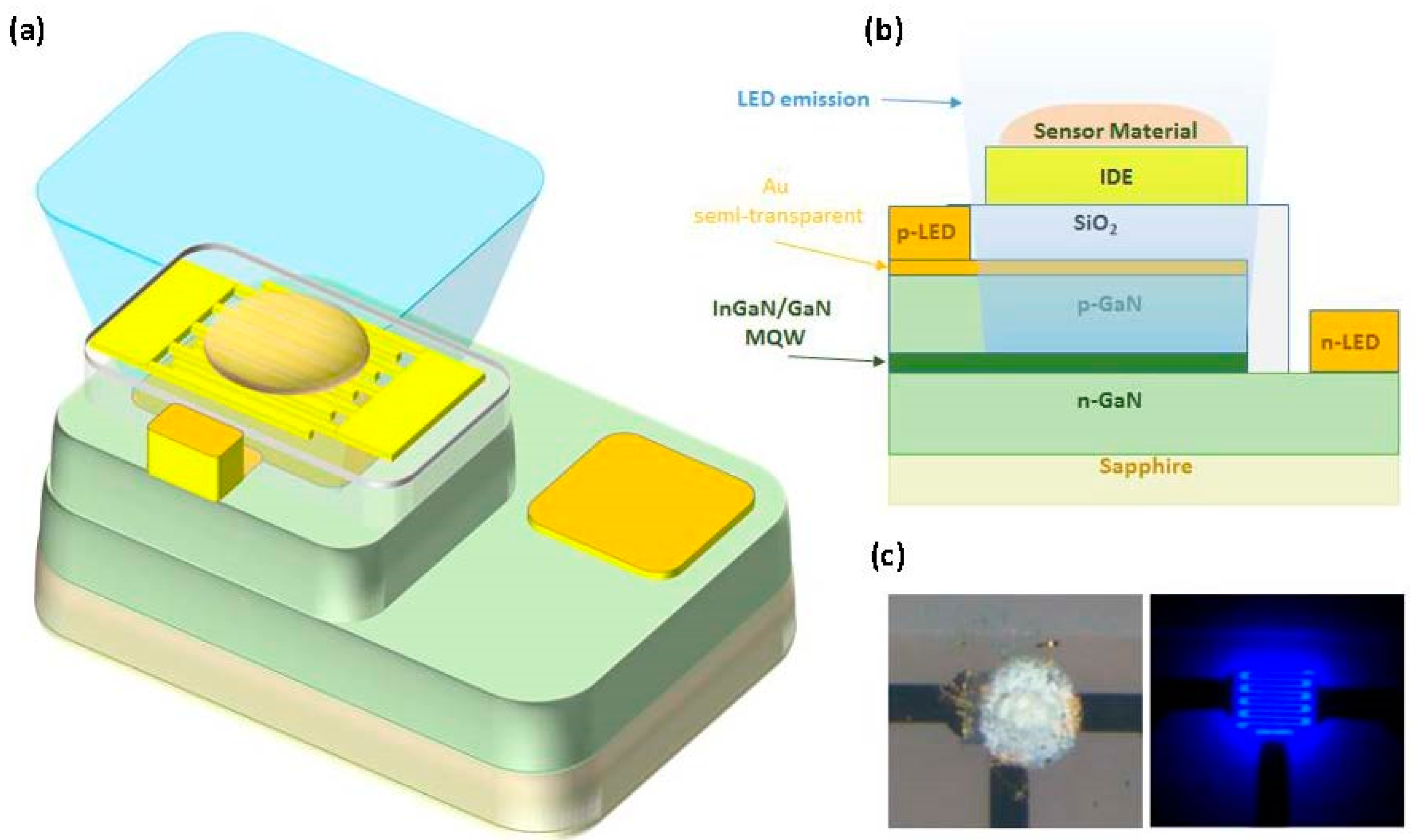
2. Materials and Methods

The devices were directly fabricated on the sapphire wafers carrying the as-grown LED structure by photolithography followed (Figure 1a,b). A mesa of the LED structure was defined by inductively coupled plasma–reactive ion (ICP-RIE) etching. The device anode was defined on the p-GaN layer of the mesa by a semitransparent layer composed by 3 nm Pd/10 nm Au and the cathode was defined on the open n-GaN layer by 30 nm Ti/300 nm Au layer, both were deposited by e-beam evaporation. The optical transmittance of the semitransparent anode was 50% at the peak emission wavelength. The IDE was also formed by the e-beam deposition of 30 nm Ti/300 nm Au layer just on the top of the p-GaN anode after the insulation of the whole mesa with an e-beam evaporated 350-nm-thick SiO2 layer (Figure 1b). The high resistivity of the p-GaN limits the light emitting area on the mesa to the area under the p-GaN anode, which allowed us to define a mesa larger than this electrode as physical support for pads (30 nm Ti/100 nm Al/30 nm Ti/300 nm Au e-beam evaporated layer) to the anode and to the IDE (Figure 1a). These enlarged pad areas facilitated the electrical access to the contacts by means of wire-bonding, without increasing the active area of the device. The area of the p-GaN anode (Figure 1b,c) was minimized as much as possible in order to minimize the power consumption but allowing for a convenient integration of the IDE and the subsequent deposition of the sensor material. In our case, that trade off was found to be in 190 × 250 µm2.

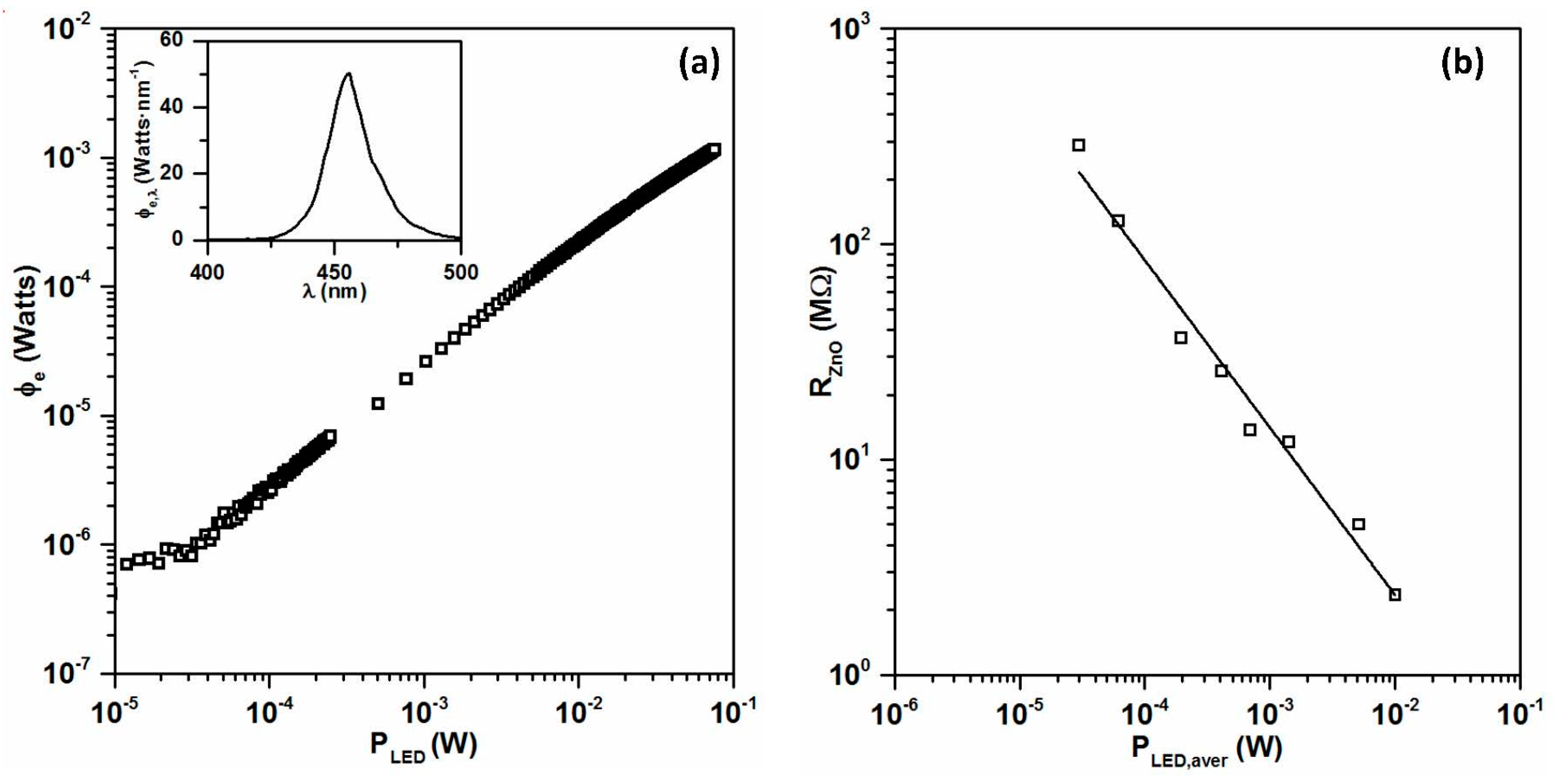
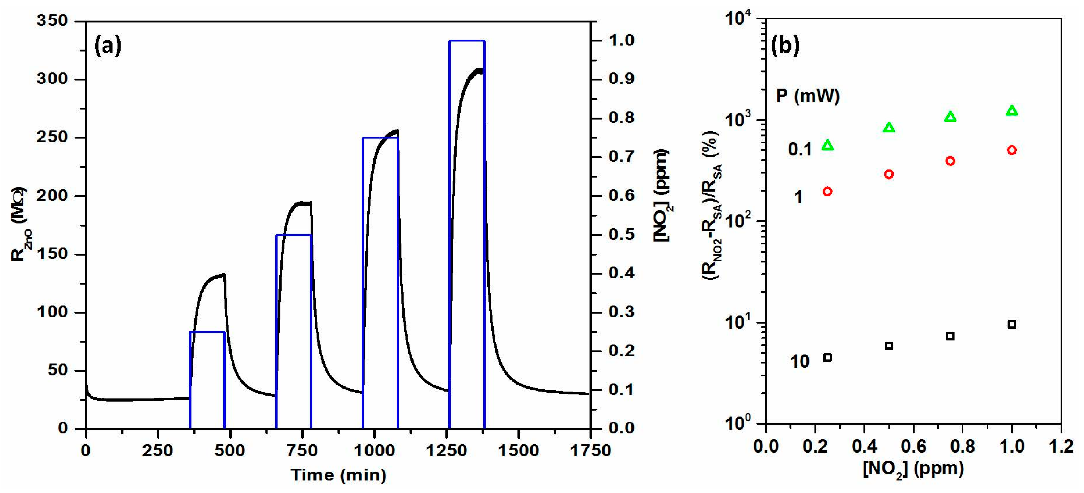
3. Results and Discussion

The final devices had thus 4 contact pads, 2 for the LED (anode (+) and cathode (−) electrodes) and 2 for the IDE. Electrically, the LED devices exhibited a good behavior with test failure of less than 20% (of more than 100 devices tested), an ideality factor of 1.7 ± 0.1, a contact resistance of 30   3 Ω, a turn-on voltage (Von) of 2.8 ± 0.1 V and a current density at 1V of 0.9 ± 0.1 µA·cm-2. Since the goal of the present application is the maximal reduction of the power consumption, it is more convenient the definition of the parameters of the threshold point (Vth, Ith or Pth the minimal voltage, current or power, respectively, needed for the device to start to emit light according with a CMOS-camera). The here-present devices exhibited a threshold power value of 15 ± 0.1 µW (2.34 ± 0.04 V and 6.4 ± 0.1 µA). The electrical insulation between the IDE electrodes and the underlying LED anode was better than 10 GΩ·cm (at 250 V/µm, ~90 V) with a field breakdown greater than 3 MV/cm (~110 V).
Figure 2. (a) Emission characteristics of the LEDs (relationship between electrical power PLED and φe power of the light emitted, and emission spectra); (b) Effect of the light emitted on the ZnO NW’s resistance (i.e., photoconductivity).
Proceedings 02 00971 g002
For demonstration purposes, we choose to build a photoactivated gas sensor based on ZnO nanowire deposited by drop casting on top of the IDE. We investigated the response to increasing concentrations of NO2 in dry air (Figure 3a), under different light intensities –and thus electrical power applied to the LED (P (Figure 3b). As expected for the interaction of a metal oxide with oxidizing species [2], the response magnitude increased with decreasing light intensities, while the response and recovery times became slower. Therefore, a tradeoff between high responses and short times must be found. As discussed in detailed in the contribution, we achieved an optimum sensor behavior with 100 µW. This is one order of magnitude lower than the best figures reported with temperature-driven sensors and several orders of magnitude better than the results working with hybrid-integrated LEDs [3].

Author Contributions

Each and every author contributed in some ways that do not need to be disclosed.

Acknowledgments

This work has been performed within EU Project of “BetterSense—Nanodevice Engineering for Better Chemical Gas Sensing Technology” funded by European Research Council under grant agreement no. 336917 and LENA-OptoSense funded by the Lower Saxony Ministry for Science and Culture (N-MWK). O. Casals agrees the support of the TecnioSpring fellowship programme of ACCIÓ, Government of Catalonia, co-funded by the EU Marie Curie Action COFUND.

Conflicts of Interest

The authors declare no conflict of interest. The founding sponsors had no role in the design of the study; in the collection, analyses, or interpretation of data; in the writing of the manuscript, and in the decision to publish the results.

References

  1. Fabrega, C.; Casals, O.; Hernandez-Ramirez, F.; Prades, J.D. A review on efficient self-heating in nanowire sensors: Prospects for very-low power devices. Sens. Actuators B Chem. 2018, 256, 797–811. [Google Scholar] [CrossRef]
  2. Prades, J.D.; Jimenez-Diaz, R.; Manzanares, M.; Hernandez-Ramirez, F.; Cirera, A.; Romano-Rodriguez, A.; Mathur, S.; Morante, J.R. A model for the response towards oxidizing gases of photoactivated sensors based on individual SnO2 nanowires. Phys. Chem. Chem. Phys. 2009, 11, 10881. [Google Scholar] [CrossRef] [PubMed]
  3. Espid, E.; Taghipour, F. UV-LED Photo-activated Chemical Gas Sensors: A Review. Crit. Rev. Solid State Mater. Sci. 2017, 42, 416–432. [Google Scholar] [CrossRef]
Figure 1. LED platform. (a,b) 3D view and cross-section of the design, including the substrate, the LED structure and its contacts and insulation layers, topped with the IDE electrodes and the sensor material. Light is emitted directly beaming the IDE region. (c) Microscope images of (left) the finished device with the ZnO nanowires deposited on top and (right) the LED lit on and emitting only under the IDE (before depositing the material).
Proceedings 02 00971 g001
Figure 3. Response to NO2. (a) Record of the ZnO NW’s resistance over time upon exposure to sub-ppm concentrations of NO2. (b) Summary of the responses obtained under different electrical powers levels applied to the LED.
Proceedings 02 00971 g003
Publisher’s Note: MDPI stays neutral with regard to jurisdictional claims in published maps and institutional affiliations.

