1. Introduction
The precise measurement of physical quantities is required in numerous safety-critical applications and therefore performed by highly accurate sensor interface circuits. Unfortunately, non-ideal influences can affect the signal processing inside the interface, which is especially true for the analog part of the system. In order to compensate these effects, different methods exist. While noise, mismatch- and offset-errors can be suppressed by complex circuit topologies, different design techniques or additional components [
1,
2], influences from process variation, varying temperature or varying supply voltage (PVT influences) can be conquered by a complementary circuit design or special layout techniques [
3,
4]. Nevertheless, all of these methods significantly increase the design time and costs of the interface. In order to overcome these drawbacks, a digital calibration based approach is chosen in this work and applied to a capacitive sensor interface [
5].
In the first step of this approach, time-division multiplexing is used to fed a suitable test signal into the sensor interface. After the test signal has passed the interface, adaptive filters are evaluating variations of it and determine present gain- and offset-errors. In this way, two correction parameters can be found and used to eliminate these errors. Since the process is operating continuously, an on-line error correction is realized, which can be used to correct static as well as time-variant errors resulting from different non-idealities. Furthermore, the design requirements of the analog circuit components can be relaxed since not all errors need to be fully compensated in the analog domain.
2. Sensor Interface Circuit
In this work, a capacitive sensor interface is used, whose analog part is shown in
Figure 1. The interface is implemented in switch-capacitor (SC) technology and consists of a Capacitance-to- Voltage converter (C/V-stage), an amplifier stage and an Analog-to-Digital Converter (ADC). It also consists of two inputs: one for the actual sensor signal and one for the test signal, which is needed for error detection. While the sensor signal is created by a capacitive acceleration sensor (ST LSM6DSL) the sinusoidal test signal is created by a configurable voltage source. In order to guarantee a proper error detection, both signals have to be transmitted through the interface separately and without interfering each other. This is realized by modifying the switching scheme of the SC-circuit to realize time-division multiplexing. The resulting switching scheme is shown in
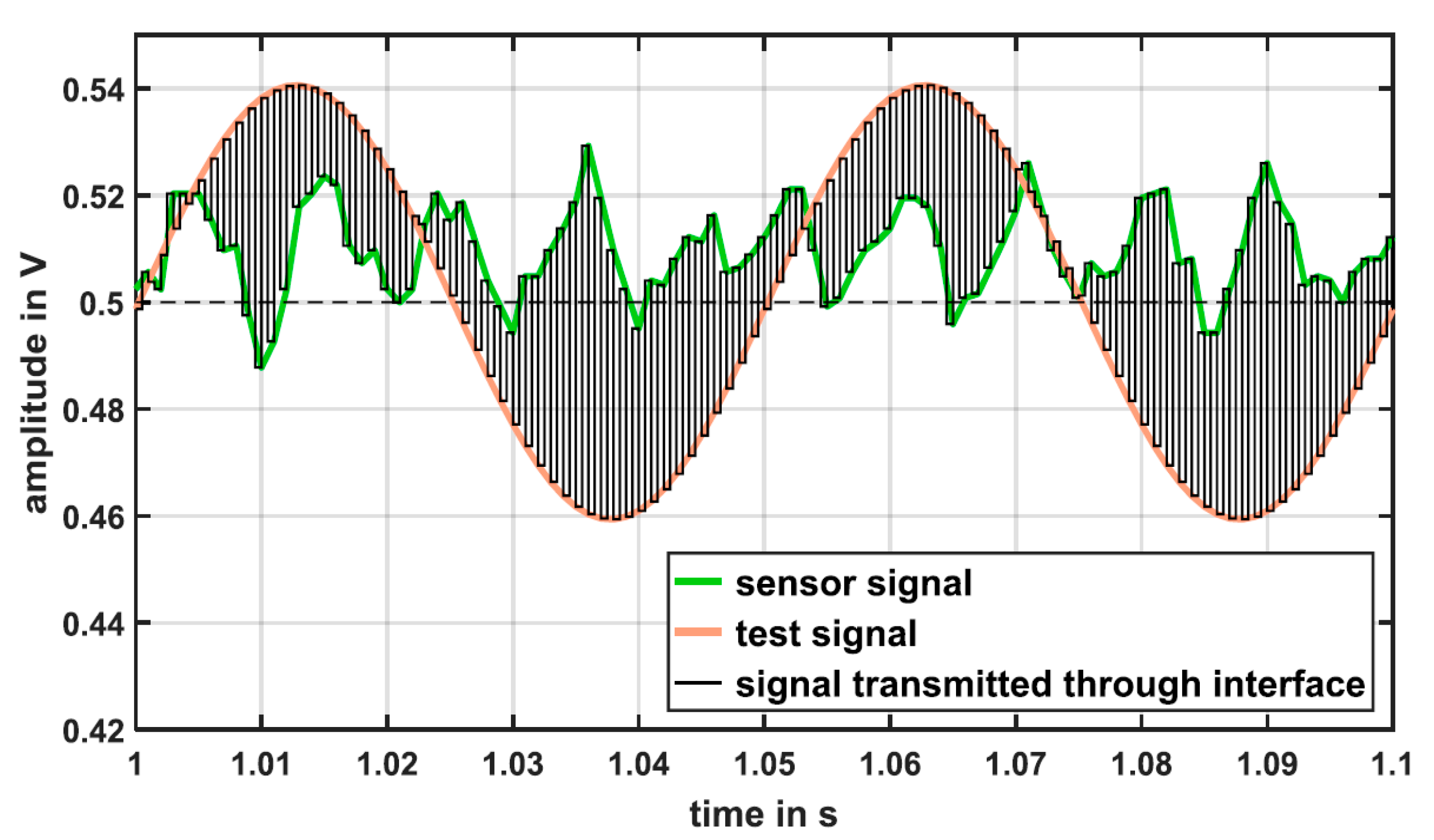
Figure 2. It can be seen that the clock phases S1, S2 and S3 are needed to operate the sensor interface, while the clock phases S4 and S5 are added to implement the multiplexer. The signal, which is created in this way and transmitted through the interface circuit is illustrated in
Figure 3.
In order to demonstrate the performance of the proposed on-line error correction, very simple circuit components are used inside the interface. Especially the switches and operational amplifiers are highly susceptible to non-ideal effects and cause different gain- and offset-errors, which result from mismatch, charge injection, clock feedthrough, charge leakage as well as the dependency on temperature and the supply voltage.
3. On-Line Error Correction by Adaptive Filtering
A novel concept based on digital calibration is used in this work to integrate an on-line error correction into a sensor interface. In this approach, the procedure of error correction is separated into three parts: the detection, the determination and the correction of present gain- and offset-errors.
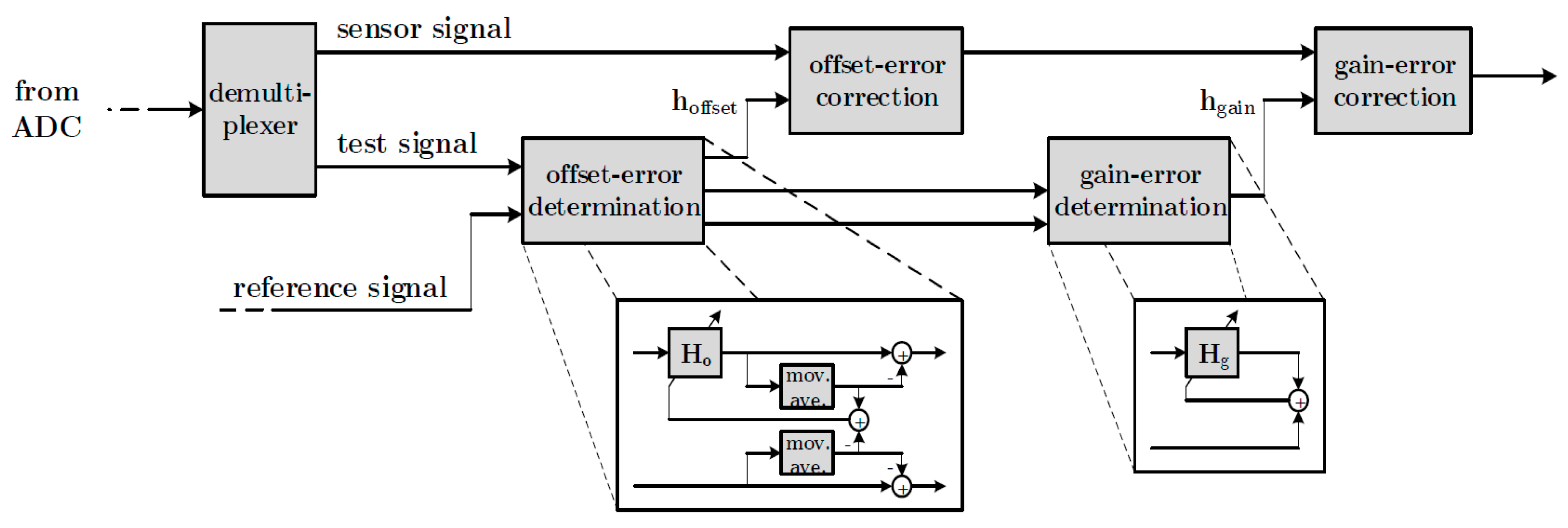
The detection of errors is performed by a suitable and well-known test signal, which makes different errors visible. It is fed into and passes the sensor interface in parallel to the sensor signal as described in the previous section. The subsequent determination and correction of errors take place in the digital part of the interface, which is shown in
Figure 4. After the sensor signal and the test signal have been digitized by the ADC, both signals are separated again by a demultiplexer. Subsequently, the test signal is compared to a reference signal, which corresponds to the output signal of the interface if no errors are present. In this process, offset-errors are determined first by comparing the moving averages of the test signal and the reference signal. This task is performed by an adaptive filter, which continuously adapts the test signal until the offset-error is completely determined and eliminated from it. In this way, a correction parameter h
offset is found, which corresponds to the present offset-error. It is handed over to another adaptive filter, which is placed in the signal path of the sensor signal and used to eliminate the offset-error from the sensor signal.
After the offset-errors are fully determined, the moving averages of the test signal and the reference signal are subtracted from them to get average-free signals. These signals are utilized afterwards to determine present gain-errors by comparing both signals. As in the case of the offset- error correction, an adaptive filter continuously adapts the test signal until the gain-error is eliminated and a second correction parameter hgain is found. This parameter is used in a second adaptive filter to correct the sensor signal.
The determination of the errors inside the adaptive filters is performed by a suitable adaptation algorithm. Either the Least-Mean-Square (LMS), the Normalized-LMS (NLMS) or the Recursive Least-Squares (RLS) algorithm are eligible for this task [
6]. Furthermore, the on-line error determination and correction are operating continuously even after the required correction parameters have been found. Thus, it becomes possible to correct static as well as time-variant gain- and offset-errors and to monitor any variations of these errors.
4. Simulation Results
The successful application of the proposed concept is shown in two different simulation scenarios. In both scenarios the sensor signal is created by a capacitive acceleration sensor and a sinusoidal test signal with an amplitude of 50 mV and a frequency of 20 Hz is used.
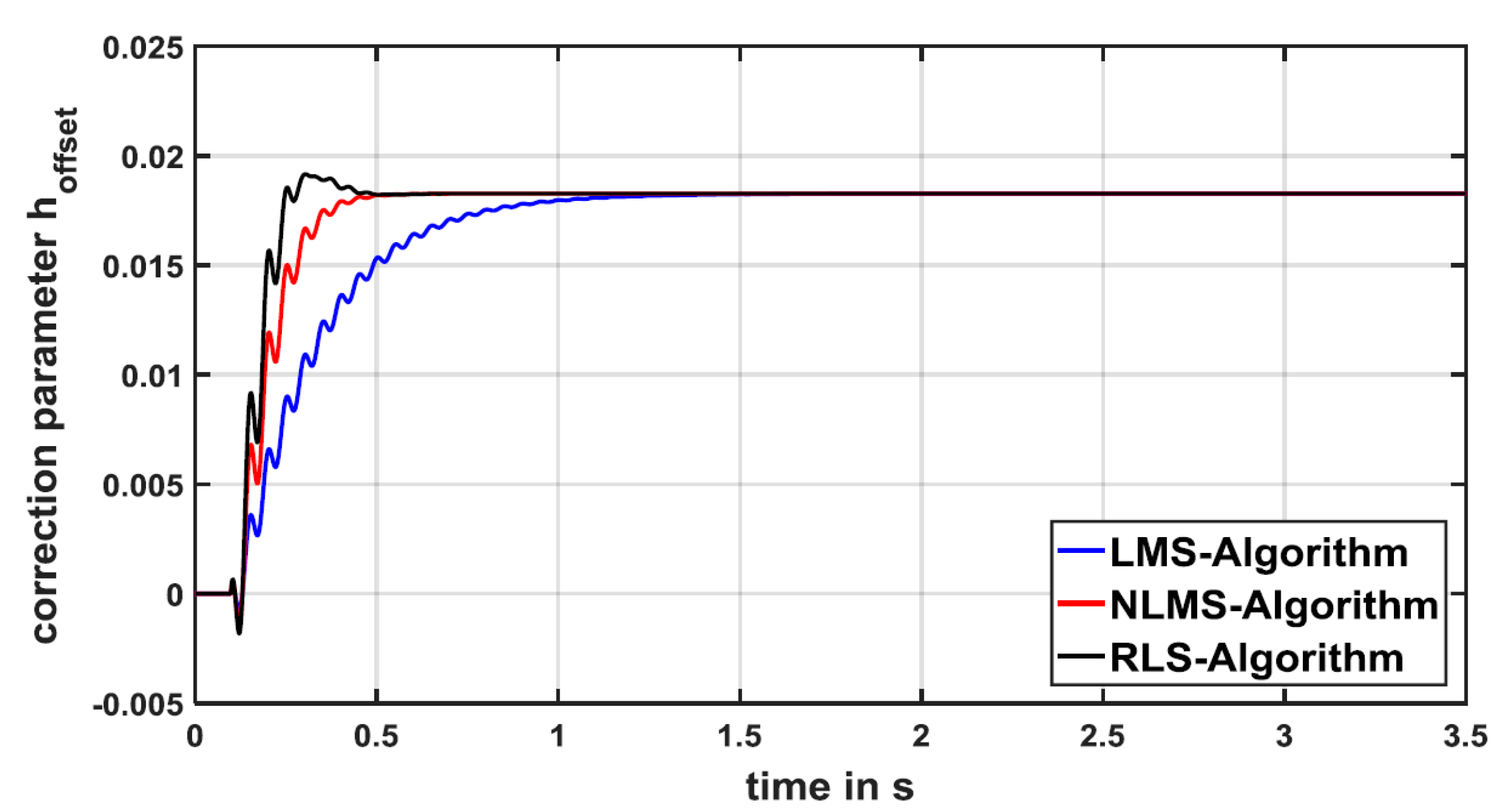
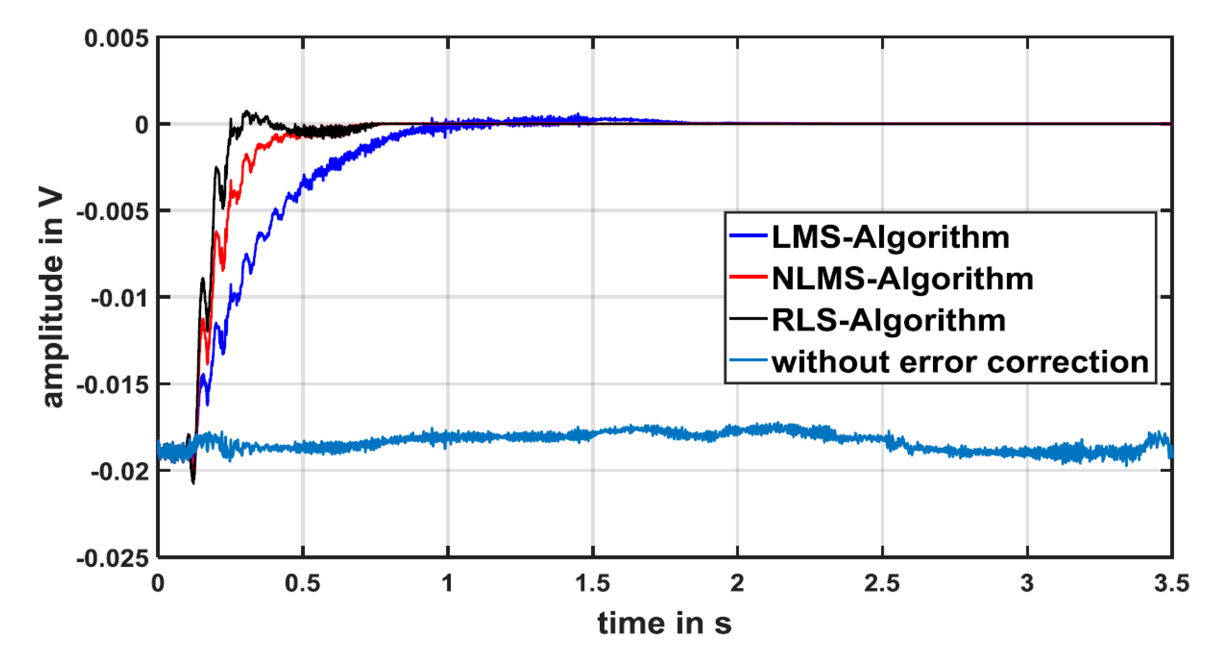
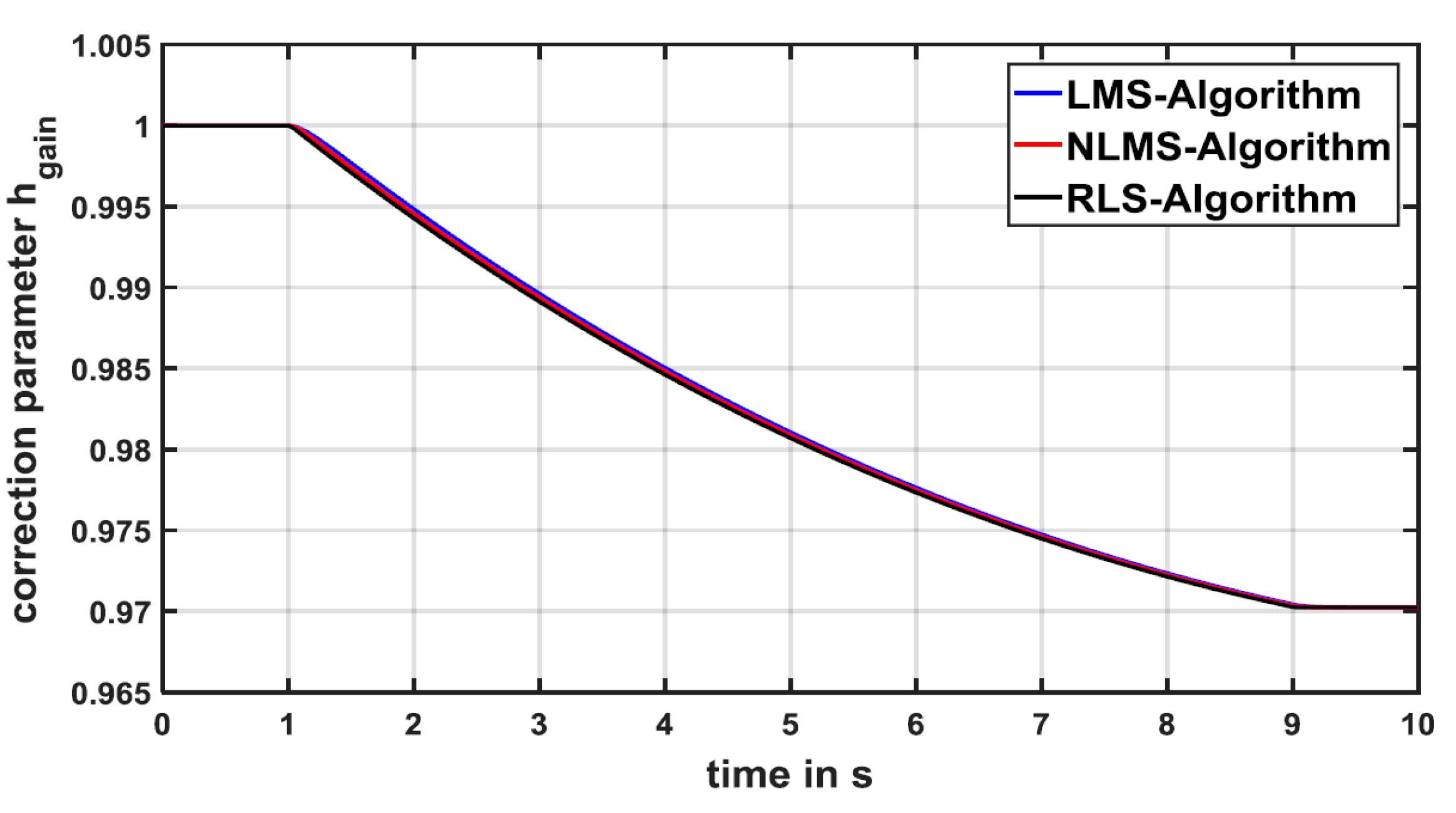
In the first simulation scenario, it is assumed that two static errors are present. An offset-error results from charge leakage at the capacitance C
12 and a gain-error results from the fact that the sensor interface is operated at a temperature of 100 °C. In order to determine the required correction parameters h
offset and h
gain, the LMS-, the NLMS- and the RLS-algorithm are utilized. The adaptation processes of these parameters are shown in
Figure 5 and
Figure 6. In addition, the error in the output signal of the sensor interface is illustrated in
Figure 7 with and without error correction. It can be seen from this figures that both errors are detected and eliminated correctly and that the error in the output of the interface is drastically reduced after a short initialization time.
In the second simulation scenario, the sensor interface is assumed to suffer from a time-variant gain-error, which results from a supply voltage drop. In order to simulate this case, the supply voltage is decreased linearly from 1 V to 0.9 V over a period of 8 seconds. The corresponding adaptation process of the correction parameter h
gain is presented in
Figure 8. As in the first simulation, the parameter and its variation are determined correctly and the gain-error is successful eliminated during the complete simulation.
5. Conclusions
An innovative concept of on-line error determination and correction is presented in this work, which uses a suitable test signal to detect static as well as dynamic gain- and offset-errors in a capacitive sensor interface. In this way, the design requirements of the analog circuit components can be relaxed, the whole system becomes more robust and variations of the circuit behavior can be monitored. Additionally, normal sensor activities are not interfered by this method since the test signal is transmitted through the interface by using time-division multiplexing. The concept of on-line error correction is also not limited to sensor interface circuits and can be applied to other mixed-signal systems. The successful application of this concept is shown by correcting various gain- and offset-errors in two different simulation scenarios.
Acknowledgments
This research project (RoMulus) is supported by the Federal Ministry of Education and Research, Germany, under reference number 16ES0362-72K.
Conflicts of Interest
The authors declare no conflict of interest. The founding sponsors had no role in the design of the study; in the collection, analyses, or interpretation of data; in the writing of the manuscript, and in the decision to publish the results.
References
- Petkov, V.; Balachandran, G.; Beintner, J. A Fully Differential Charge-Balanced Accelerometer for Electronic Stability Control. IEEE J. Solid-State Circ. 2014, 49, 262–270. [Google Scholar] [CrossRef]
- Bracke, W.; Merken, P.; Puers, R.; van Hoof, C. Ultra-Low-Power Interface Chip for Autonomous Capacitive Sensor Systems. IEEE Trans. Circ. Syst. I Regul. Pap. 2007, 54, 130–140. [Google Scholar] [CrossRef]
- Wang, Y.; Chan, P.K.; Li, K.H. A Compact CMOS Ring Oscillator with Temperature and Supply Compensation for Sensor Applications. In Proceedings of the 2014 IEEE Computer Society Annual Symposium on VLSI, Tampa, FL, USA, 9–11 July 2014; pp. 267–272. [Google Scholar]
- Baker, R.J. CMOS Circuit Design, Layout, and Simulation, 3rd ed.; Wiley-IEEE Press: Hoboken, NJ, USA, 2010. [Google Scholar]
- Murmann, B. Digitally Assisted Data Converter Design. In Proceedings of the ESSCIRC, Bucharest, Romania, 16–20 September 2013; pp. 24–31. [Google Scholar]
- Haykin, S. Adaptive Filter Theory, 5th ed.; Addison Wesley Pub Co Inc.: Boston, MA, USA, 2013. [Google Scholar]
| Publisher’s Note: MDPI stays neutral with regard to jurisdictional claims in published maps and institutional affiliations. |
© 2018 by the authors. Licensee MDPI, Basel, Switzerland. This article is an open access article distributed under the terms and conditions of the Creative Commons Attribution (CC BY) license (https://creativecommons.org/licenses/by/4.0/).
