Abstract
Light-addressable potentiometric sensors (LAPS) measure ac photocurrent at electrolyte-insulator-semiconductor (EIS) and, more recently, electrolyte-semiconductor structures to produce spatiotemporal images of chemical or biological analytes, electrical potentials and impedance. One of the most important properties for LAPS is spatial resolution, which determines the smallest features that can be resolved in LAPS images. In this work, the use of nanostructured ZnO for LAPS was explored. The effect of ZnO morphology on the spatial resolution was studied with a LAPS setup. The best resolution of 2 µm was achieved in ZnO films produced by aerosol-assisted chemical vapour deposition (AACVD).
1. Introduction
LAPS were first introduced by Hafeman et al. using an EIS structure, in which an insulator-semiconductor structure is in contact with the solution to be analysed [1]. More recently, electrolyte-semiconductor structures have been shown to be suitable for LAPS imaging [2,3]. There is a growing drive to develop LAPS for biological applications such as the monitoring of concentrations in microfluidic channels or the investigation of metabolic and signalling events in living cells [4,5,6,7]. Imaging technology is crucial to many disciplines and is generally classified as optical imaging, electronic imaging or a combination of both. LAPS photocurrent imaging belongs to the family of electronic imaging technology, in which the spatial distribution of analytes or physiological events in cellular processes can be visualized.
Resolution is one of the most important properties of an image. The spatial resolution in LAPS is defined as the diffusion length within the lifetime of the minority carriers, for example holes in n-type semiconductors. It is determined by two main factors, which are (1) the lateral diffusion of minority carriers out of the illuminated area in the semiconductor and (2) the quality of the light focus for charge carrier excitation.
Improvements in LAPS resolution have been widely explored. Nakao et al. reported that the spatial resolution of 300 µm was improved to 10 µm by decreasing the thickness of the silicon from 500 to 20 µm [8]. However, this method is limited as thin silicon substrates are fragile and difficult to process. Ito solved this problem by replacing the fragile silicon with silicon-on-sapphire (SOS), in which the active layer was only 500 nm thick [9]. Krause et al. reported the best resolution for LAPS to date of 0.8 µm by using a 500 nm thick silicon layer on sapphire and a two-photon effect for photocurrent excitation [10]. Therefore, thinning the semiconductor substrate is an effective method to decrease the minimum pattern for LAPS to resolve. To find a suitable semiconductor with a smaller minority carrier diffusion length would be a different strategy for improving the resolution. The diffusion length of minority charge carriers in bulk ZnO is 0.13–0.44 µm [11], which is several orders of magnitude smaller than in p-type silicon. ZnO, a n-type semiconductor with a direct band gap has the advantage of low cost, easy synthesis, ability to control its morphology and biocompatibility [12,13,14]. It has been applied in energy harvesting systems, photocatalysts, and chemical sensors. In this work, ZnO nanorods and films were used in LAPS to study the effect of morphology on spatial resolution.
2. Materials and Methods
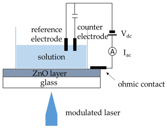
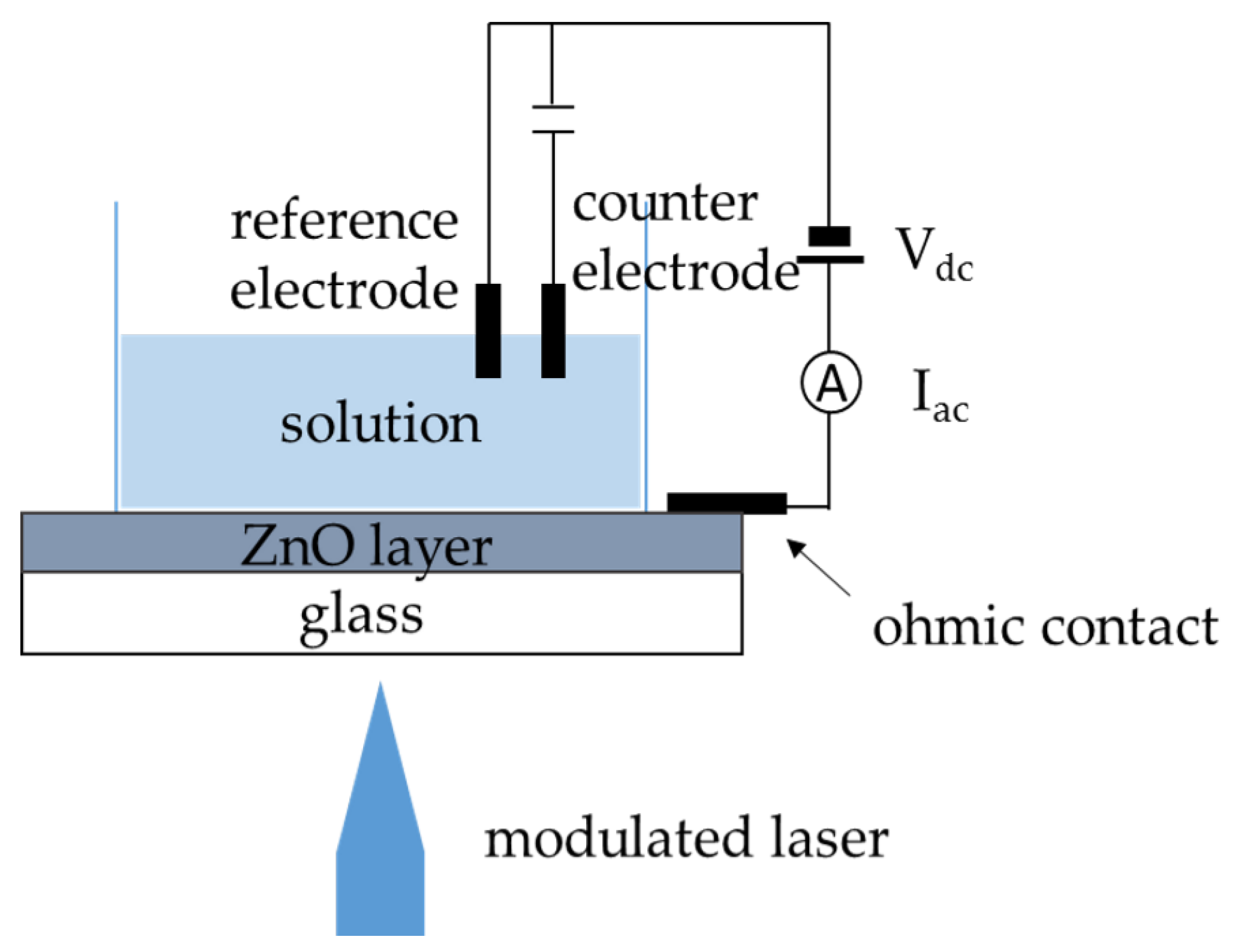
All the chemicals were used without further purification. ZnO was synthesized on FTO-coated glass (1 cm × 1 cm, 15 Ω/sq, Solaronix SA, Aubonne, Switzerland). The substrates were cleaned using acetone (VWR Chemicals, 100%, Lutterworth, UK) and 2-propanol (VWR Chemicals, 100%, Lutterworth, UK) in an ultrasonic bath for 15 min each. ZnO nanorods were synthesized using an aqueous solution method reported previously [15]. ZnO films were produced by increasing the precursor concentration to 100 mM using the same recipe as for the nanorods. For AACVD ZnO, the laboratory aerosol assisted chemical vapour deposition (AACVD) set-up is illustrated in [16]. The AACVD precursor was prepared by dissolving 0.4 g zinc acetate dihydrate in 25 mL methanol. The substrates were placed on a graphite block in the reactor and preheated to 450 °C. The as-prepared precursor solutions were transferred to a Drechsel bottle, and then an ultrasonic humidifier with operating frequency of 1.6 MHz generated an aerosol mist. The mist was continuously passed through the reaction chamber with nitrogen carrier gas at 1.5 L/min until exhausted. The carrier gas was kept flowing until the temperature of the reactor chamber dropped below 80 °C. The total deposition time was 45 ± 5 min. A drop of a 11 wt % PMMA solution in methoxybenzene was deposited on ZnO and dried without assistance at room temperature. The LAPS measurement setup was described in [2] and a schematic is shown in Figure 1.

Figure 1.
Schematic of a simplified LAPS setup.
3. Results and Discussion
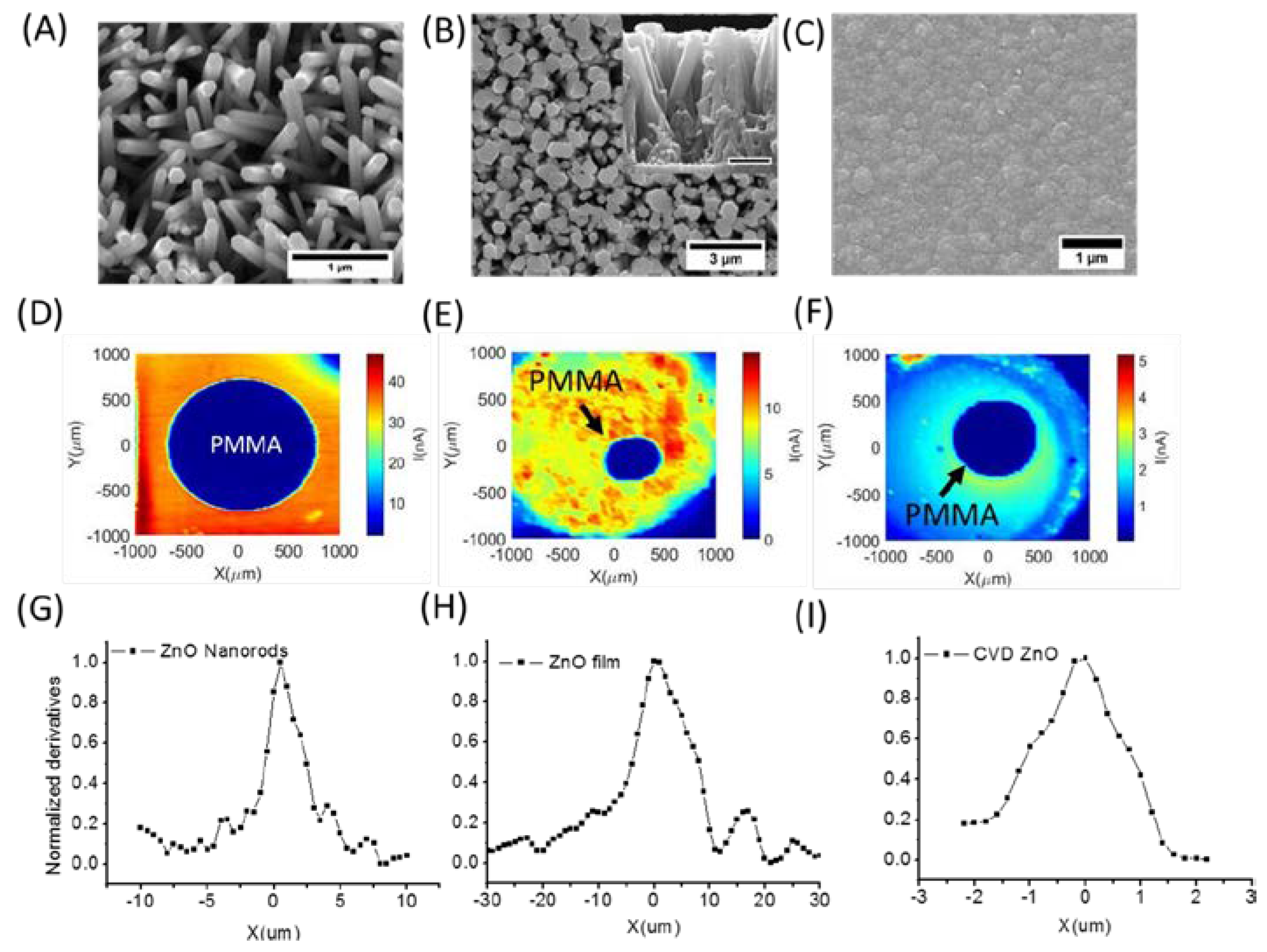
Figure 2A–C display the morphology of ZnO made with different methods. The nanorods formed uniformly and were well-oriented with 4.03 ± 0.025 µm in length and 78.4 ± 2.7 nm in diameter. The film in (B) formed columns with much larger diameters in a range of 0.3 to 0.9 µm, which were mostly fused together in a film-like structure (inset Figure 2B) with some gaps still visible in the top view. For comparison, ZnO nanorods and films made with the solution method had the same thickness. ZnO made with AACVD formed a compact film with 1 µm thickness (Figure 2C). Figure 2D–F show photocurrent images with a PMMA dot on the surface of ZnO. Table 1 summarises the maximum photocurrent and spatial resolution in different morphologies. The photocurrent measured on the uncoated areas was much greater on the nanorods than on the film, and the AACVD ZnO film had the lowest photocurrent at a light intensity of 0.05 mW. This is ascribed to the significant larger surface area of the nanorods compared to the film and the CVD ZnO. However, the spatial resolution (FWHM of the first derivative of a photocurrent line scan across the edge of the PMMA dot) in Figure 2G–I did not follow the same trend as the maximum photocurrent, in that the best resolution of 2 µm was obtained for the CVD ZnO followed by the ZnO nanorods with 3 µm resolution and the solution grown film with the poorest resolution of 12 µm. The minority diffusion length in ZnO is shorter than 1 µm, i.e., lateral diffusion of minority carriers cannot explain any differences in resolution between the different morphologies. As the wavelength of the light used in all the LAPS measurements was 405 nm, it is likely that light scattering effects played a significant role in the degradation of the resolution in the solution grown ZnO film because the columns in the film are larger than the wavelength of light. Light scattering effects in ZnO nanorods were negligible as their diameter was significantly smaller than 405 nm, thereby resulting in a better resolution. Light scattering effects for CVD films were negligible because of their small crystal size. As the AACVD films were four times thinner than the ZnO nanorods, they showed a somewhat improved resolution. In conclusion, the morphology of nanostructured ZnO has a significant effect on the spatial resolution in LAPS images due to the thickness of the sensing layer and light scattering effects.

Figure 2.
SEM images of (A) ZnO nanorods, (B) solution made ZnO film (inset cross-sectional view (scale bar 1 µm)) and (C) CVD ZnO, (D–F) the corresponding LAPS images with a PMMA dot (indicated), (G–I) the corresponding first derivatives of photocurrent line scans across the edge of the PMMA dots.

Table 1.
Maximum photocurrent and spatial resolution of ZnO in different morphologies.
Acknowledgments
The authors thank the Biotechnology and Biological Sciences Research Council (BBSRC) of UK for providing research funding (BB/P026788/1), the EU for providing a Marie Skłodowska-Curie Individual Fellowship (H2020-MSCA-IF-2014-660489) and the China Scholarship Council (CSC) for providing a PhD studentship to Y.T.
Conflicts of Interest
The authors declare no conflict of interest.
References
- Hafeman, D.G.; Parce, J.W.; Mcconnell, H.M. Light-Addressable Potentiometric. Science 1988, 240, 1182–1185. [Google Scholar] [CrossRef] [PubMed]
- Zhang, D.-W.; Wu, F.; Krause, S. LAPS and SPIM Imaging Using ITO-Coated Glass as the Substrate Material. Anal. Chem. 2017, 89, 8129–8133. [Google Scholar] [CrossRef] [PubMed]
- Tu, Y.; Ahmad, N.; Briscoe, J.; Zhang, D.-W.; Krause, S. Light-Addressable Potentiometric Sensors Using ZnO Nanorods as the Sensor Substrate for Bioanalytical Applications. Anal. Chem. 2018, 90, 8708–8715. [Google Scholar] [CrossRef] [PubMed]
- Yoshinobu, T.; Miyamoto, K.; Werner, C.F.; Poghossian, A.; Wagner, T.; Schöning, M.J. Light-Addressable Potentiometric Sensors for Quantitative Spatial Imaging of Chemical Species. Annu. Rev. Anal. Chem. 2017, 10, 225–246. [Google Scholar] [CrossRef] [PubMed]
- Wu, F.; Campos, I.; Zhang, D.-W.; Krause, S. Biological imaging using light-addressable potentiometric sensors and scanning photo-induced impedance microscopy. Proc. R. Soc. A Math. Phys. Eng. Sci. 2017, 473, 1–20. [Google Scholar] [CrossRef] [PubMed]
- Zhang, D.W.; Papaioannou, N.; David, N.M.; Luo, H.; Gao, H.; Tanase, L.C.; Degousée, T.; Samorì, P.; Sapelkin, A.; Fenwick, O.; et al. Photoelectrochemical response of carbon dots (CDs) derived from chitosan and their use in electrochemical imaging. Mater. Horizons 2018, 5, 423–428. [Google Scholar] [CrossRef]
- Pohanka, M.; Leuchter, J. Biosensors based on semiconductors, a review. Int. J. Electrochem. Sci. 2017, 12, 6611–6621. [Google Scholar] [CrossRef]
- Nakao, M.; Inoue, S.; Yoshinobu, T.; Iwasaki, H. B High-resolution pH imaging sensor for microscopic observation of microorganisms. Sens. Actuators B 1996, 34, 234–239. [Google Scholar] [CrossRef]
- Ito, Y. High-spatial resolution LAPS. Sens. Actuators B Chem. 1998, 52, 107–111. [Google Scholar] [CrossRef]
- Chen, L.; Zhou, Y.; Jiang, S.; Kunze, J.; Schmuki, P.; Krause, S. High resolution LAPS and SPIM. Electrochem. Commun. 2010, 12, 758–760. [Google Scholar] [CrossRef]
- Soudi, A.; Dhakal, P.; Gu, Y. Diameter dependence of the minority carrier diffusion length in individual ZnO nanowires Electron-beam-induced current and cathodoluminescence studies of thermally activated increase for carrier diffusion length and lifetime in-type ZnO. Appl. Phys. Lett. Appl. Phys. Lett. 2010, 96, 253115. [Google Scholar] [CrossRef]
- Wang, Z.L. Nanostructures of zinc oxide. Mater. Today 2004, 7, 26–33. [Google Scholar] [CrossRef]
- Schmidt-Mende, L.; MacManus-Driscoll, J.L. ZnO—Nanostructures, defects, and devices. Mater. Today 2007, 10, 40–48. [Google Scholar] [CrossRef]
- Wang, Z.L. Zinc oxide nanostructures: Growth, properties and applications. J. Phys. Condens. Matter 2004, 16, 829–858. [Google Scholar] [CrossRef]
- Tu, Y.; Chen, S.; Li, X.; Gorbaciova, J.; Gillin, W.P.; Krause, S.; Briscoe, J. Control of oxygen vacancies in ZnO nanorods by annealing and their influence on ZnO/PEDOT: PSS diode behavior. J. Mater. Chem. C 2018, 6, 1815–1821. [Google Scholar] [CrossRef]
- Powell, M.J.; Carmalt, C.J. Aerosols: A Sustainable Route to Functional Materials. Chem. A Eur. J. 2017, 23, 15543–15552. [Google Scholar] [CrossRef]
Publisher’s Note: MDPI stays neutral with regard to jurisdictional claims in published maps and institutional affiliations. |
© 2018 by the authors. Licensee MDPI, Basel, Switzerland. This article is an open access article distributed under the terms and conditions of the Creative Commons Attribution (CC BY) license (https://creativecommons.org/licenses/by/4.0/).


